
Abstract
Tunable optical emission properties from ferromagnetic semiconductors have not been well identified yet. In this work, high-quality Mn(II)-doped CdS nanowires and micrometer belts were prepared using a controlled chemical vapor deposition technique. The Mn doping could be controlled with time, precursor concentration and temperature. These wires or belts can produce both tunable redshifted emissions and ferromagnetic responses simultaneously upon doping. The strong emission bands at 572, 651, 693, 712, 745, 768, 787 and 803 nm, due to the Mn(II) 4T1(4G) → 6A1(6s) d–d transition, can be detected and accounted for by the aggregation of Mn ions at Cd sites in the CdS lattice at high temperature. These aggregates with ferromagnetism and shifted luminescence are related to the excitonic magnetic polaron (EMP) and localized EMP formations; this is verified by ab initio calculations. The correlation between aggregation-dependent optical emissions and ferromagnetic responses not only presents a new size effect for diluted magnetic semiconductors (DMSs), but also supplies a possible way to study or modulate the ferromagnetic properties of a DMS and to fabricate spin-related photonic devices in the future.
Export citation and abstract BibTeX RIS
1. Introduction
Luminescence is an important physical property of solids and luminescence tunable is attracting researchers. Except for nonlinear optics, people have found that many related physical phenomena can work for tunable emissions. For example, the quantum confinement effect and bandgap engineering in quantum wells, quantum wires, and QDs can tune their optical emission wavelengths [1]. Bandgap shift due to alloy formation [2] and energy transfer and inner conversion between transition metal (TM) ions or rare earth metal ions also can tune the emission colors [3], as well as the conjugated molecules with varied double bonds. These physical phenomena give nice tunable emissions, but they have not been compatible with intrinsic ferromagnetic response of the material.
Semiconductors doped with small amounts of magnetic impurities, i.e., called diluted magnetic semiconductors (DMSs), have very interesting ferromagnetic properties [4–6], which usually arise from spin–carrier exchange interactions between the dopant ions and the host charge carriers (sp–d exchange interactions). Spin clustering has also been found to cause ferromagnetic responses in some semiconductors [7, 8]. TM-doped II-VI DMSs and III-V DMSs have been studied widely because TM ions can give rise to magnetic polarons [9, 10], large carrier-spin polarization, and magnetically enhanced optoelectronic effects [11]; however, full understanding of luminescence properties has still not been achieved. During the past ten years, there has been growing recognition that devices exploiting spin-polarized electrons can exhibit performance superior to conventional electronic devices [12]. Despite a huge amount of work to understand the mechanisms behind the ferromagnetism of DMSs, a generally accepted and consistent explanation for complex structures is still being discussed [13]. The relationships between d-d radiation transition and ferromagnetism in a DMS, specifically, have not been well established because the luminescence techniques are not widely used for DMS study and some DMS researchers do not relate the magnets to chromophore. From theoretical and application viewpoints, a DMS should possess the ferromagnetic and semiconductor simultaneously, so their luminescence should be its intrinsic property. Therefore, the relationship between the ferromagnetic states and exciton behaviors in a DMS should be studied. The previously reported observations of excitonic magnetic polaron (EMP) [9] and localized EMP (LEMP) or bound magnetic polaron [10, 14] were actually the start in correlating the magnetic excitations for optical properties of DMSs.
CdS, a typical II-VI compound semiconductor, is an important direct-band semiconductor with a bandgap of 2.4 eV. It can be also used as a DMS when a fraction of component ions of semiconductors is replaced by TM impurities. Most efforts have been focused on Mn-doped DMS materials. The ionic radius of Mn2+ (0.80 Å) is smaller than the radius of Cd2+ (0.95 Å) and, along with its similar chemical properties, it can substitute for Cd2+ ions in the CdS crystal lattice or become interstitial. Mn-doped CdS semiconductors have been mainly studied because of the luminescence of the Mn2+ ions inside the CdS host; their presence in a semiconductor leads to exchange interactions between s–p band electrons and manganese d electrons. Research is available on the single Mn(II) ion-related emission (usually at wavelength from 575–598 nm) of the doped II–VI semiconductor nanostructures and magnetism [15–18]; however, some studies reported that the optical emission was possibly from the Mn(II) pair or aggregates in them [16, 19–25].
Several preparation routes of CdS:Mn nanowires/belts were reported in the literature: hydrothermal, chemical solution, solvothermal, surfactant assisted, and chemical vapor deposition (CVD) methods. In this paper, we prepared high-quality Mn-doped CdS belts using the CVD method, in which we found the tunable luminescence properties of different pairs of Mn ions incorporated into a CdS host and their ferromagnetic properties at room temperature. The luminescence mechanism was also studied to correlate the Mn ion-related photoluminescence (PL) emissions to ferromagnetism. Why these phenomena occur in these nanowires/microbelts using the CVD technique but not using other preparation techniques is analyzed. To the best of our knowledge, finding a way to realize the tunable luminescence with the TM ions aggregates with ferromagnetic couplings has potential applications in spin photonics for quantum modulation and other nanophotonic devices. Here, we design a series of experiments to further the understanding of the relationship between magnetic and luminescence of DMS nanostructures. The morphology, chemical composition, and phase identification of the prepared samples were characterized through field emission scanning electron microscopy (FE-SEM), x-ray diffraction (XRD), electron paramagnetic resonance (EPR), and Raman spectra. Optical properties were studied using the micro-photoluminescence and time-correlated single photon counting system, and magnetic properties were studied using the superconducting quantum interference device (SQUID) and MFM.
2. Experimental details
Mn-doped CdS belts were synthesized through thermal evaporation in a horizontal tube furnace. A horizontal quartz tube was mounted inside a high-temperature tube furnace. A 2 g mixture of CdS powder (99.995%, Aldrich) and MnCl2 powder (99.99%, Aldrich) with a ratio of 1:01 (atomic weight) was loaded into a ceramic boat and inserted into the central region of the quartz tube. Ultrasonically cleaned Si wafers were used as substrates for the deposition of nanostructures and gold-plated (∼10 nm) silicon wafers were put in place under the airflow about 15 cm away from the center of quartz tube. After the tube had been purged with Ar (99.999%) premixed with H2 (10%) for two hours, the resource temperature was raised to 860 °C and was held at that temperature for 50 min before returning to room temperature. During the growth process, the carrier gas flow was kept at a constant rate of 60–80 sccm. After the reaction, a light yellow colored product was obtained on the Si substrates. Details of the characterization techniques used in preceding results are available in the supporting information.
3. Results and discussions
The morphologies of the as-prepared Mn-doped CdS belts were observed with FE-SEM, as shown in figures 1(a) and (b) for low- and high-magnification, respectively. Figures 1(a) and (b) indicate that the surfaces of the belts are smooth, with an average length and width of about 60–140 μm and 1–1.5 μm, respectively, and thickness of 100–150 nm (shown as inset in figure 1(b)). It is clear from figure 1(a) that the belt width decreases gradually along the growth direction, terminates with a particle at the tip, which indicates that a gold-catalyzed nanowire growth by vapor–liquid–solid (VLS) process occurs ab initio, and then grows the belts through the vapor–solid (VS) process. Both the CVD technique and micrometer size are important for our study. The high temperature in CVD growth for a definite time can cause ion diffusion and aggregation within the crystal lattice, which can lead to a high aggregation degree if enough ion precursors were used. This aggregation occurs without lattice change, but does not produce a new phase in the matrix. This aggregation process is described in figure S1. Clearly, such aggregate formation can give different properties in contrast to the system with individual ion doping. For the micrometer size structure for multi-ions doping, ion diffusion can occur to produce aggregate inside, but not to segregate on the surface. If this occurs in a nanocrystal, the dopant ions may easily move from the surface at high temperature, which would lead to a new phase segregating. For quantum dots prepared using the solution method, such high aggregation would prevent the dots from forming due to small size and easy surface segregation [19, 21–23]. For example, the doping Mn ions can eject out of QD easily even at below 300 °C [19, 25], and the doped nanorod using the solution method can form an aggregate of two Mn ions at most [24]. TM ions in one semiconductor belt can inevitably form aggregate at close 900 °C. Hence, up to micrometer size, high temperature is necessary for the production of multi-ion aggregate doped DMS microstructure, which is important for further optical and magnetic study.
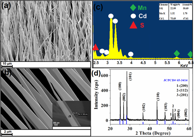
Figure 1. (a) Low- and (b) high-magnification FE-SEM images of CdS:Mn belts and (c) the corresponding EDX spectrum measured from a point in a belt. (d) XRD patterns of the as-grown Mn-doped CdS belts.
Download figure:
Standard image High-resolution imageTo examine the elemental composition of the belts, energy-dispersive x-ray (EDX) measurements were performed on the as-grown belt (figure 1(c)). The data in figure 1(c) show that the belts are composed of only three elements: Cd, S, and Mn. The highest Mn concentration was 1.70% (atomic ratio) in our sample, even if a mixed precursor powder of CdS: MnCl2 = 12 in weight ratio was used. The powder x-ray diffraction pattern (figure 1(d)) shows that Mn-doped CdS belts have the single-phase wurtzite hexagonal structures. All the XRD peaks of the undoped CdS NWs (not shown here) exactly matches with the Joint Committee on Powder Diffraction Standards (JCPDS) card No. 65–3414 for wurtzite hexagonal phase of bulk CdS. It can be confirmed from figure 1(d) that peaks position at 2θ = 24.8, 26.5 and 28.2° shifts slightly to the higher angles indicating a lattice distortion because of the introduction of dopant i.e., Mn. No diffraction peaks from other impurities were detected because only about 1.70% (atomic ratio) of Mn was detected (figure 1(c)). Typical two-dimensional (2D) elemental mappings of the CdS:Mn2+ belt are shown in figures S2(a)–(d). These mappings clearly show that Mn2+ is almost homogenously distributed in the CdS nanobelt, i.e., Mn2+ ions are almost dispersed in CdS crystal lattice uniformly in small selected area. But for the longer one, we can see that Mn concentration decreases with the growth of the belts, i.e., Mn concentration in the root side of a belt is a little larger than that in the tip side (figures S2(e)–(i)); the incorporation of Mn has slight higher efficiency at the start stage than that at the later stage of the growth reaction.
Raman spectroscopy was employed for the investigation of the atomic arrangement changes of CdS crystal lattice upon Mn2+ doping. Figures S3(a) and (b) show room temperature Raman spectra of the bulk (powders) CdS deposited on the silicon wafer and Mn2+-doped CdS belt. Five vibrational modes are observed, as listed in table S1, for the bulk (powders) CdS and the doped-CdS belt. These modes are attributed to the multiphonon scattering; i.e., first-order transverse optical (TO), E1(TO), E2, and the first-and second-order longitudinal optical (LO) phonon modes of CdS [26, 27]. It is noticed that there is clear splitting for the 1LO phonon (shown in inset of figure S3(b)) mode and dominant 2LO phonon mode in the doped belt. Using a multi-peak Gauss fitting at 1LO, we obtained two Gaussian curves, namely GFC1 and GFC2. The peak positions of GFC1 and GFC2 are at 300.9 and 309.5 cm−1, respectively. The peak position of GFC1 is close to the 1LO phonon of CdS. This splitting at GFC1 and GFC2 can be accounted for by the lattice distortion by Mn ion incorporation [28], which occurs because of the reduction of 1LO mode symmetry and its long range axial polarization. The 2LO peak comes from larger photon–phonon interaction with a longer photonic propagation distance in the belt than that in the powder [29].
Figure 2(a) shows room temperature photoluminescence spectra of undoped CdS and Mn(II)-doped single belts, which are prepared under the same growth conditions as stated previously; their emission lifetime decay profiles are depicted in figure 2(b). The belts are excited by continuous-wave (CW) semiconductor laser pulses at 405 nm. For the Mn-doped CdS belts, the same PL spectra can also be obtained using 532 nm laser excitation. The room temperature PL spectra of different CdS:Mn belts in figure 2(a) show emission maxima at 572, 651, 693, 712, 745, 768, 787, and 803 nm, respectively. The room temperature green emission band at about 508 nm for pure CdS is assigned to the band-edge emission, but in ferromagnetic CdS it often shows up at wavelengths longer than 510 nm, even upto 518 nm for the EMP formation [9]. The latter is an excitation of free exciton combined with ferromagnetic clouds, whose energy is just slightly smaller than that of the exciton. The d-d transition, previously considered one excitation, occurs within doping a TM ion in a solid [15, 18, 20]. Recently, researchers found that it might become a LEMP because of the p-d hybridization and ferromagnetic coupling [9, 10, 14]. The yellow band, located at about 572 nm, is the emission band from a single Mn2+ in Mn-doped II-VI semiconductors, as reported at 576–598 nm, which is assigned to d–d transition between the 4T1(4G) excited state and the 6A1(6s) ground state of Mn2+ (as the electronic levels shown in figure S6) [15, 18, 19, 21]. It is interesting to note that if we increase the Mn(II) doping concentration, we find that more emission bands shift to red in our samples under varied growth conditions. These peaks can appear independently at a 532 nm excitation level and coexist with the 515 nm band at 405 nm excitation. Sometimes several peaks can simultaneously appear for one belt (as shown in figure S7). Figure S8 presents images with different emission colors from one belt or wire under 405 nm excitation; yellow, orange, and red colors can be easily seen, but the infrared band over 750–900 nm can be only found by the spectrometer.
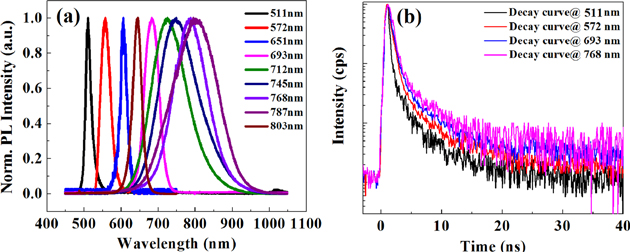
Figure 2. (a) PL spectra of the obtained single undoped CdS and Mn2+-doped CdS belt at 300 K. The black line is from the pure CdS belt and the other lines are from the emission of CdS doped with different Mn ions. (b) PL lifetime decay plots for the band-edge emission along with Mn2+ related emissions at room temperature in a Mn-doped CdS single belt. The pulse excitation wavelength was 405 nm.
Download figure:
Standard image High-resolution imageDifferent authors have given different explanations for the red emission band near 646 nm. Some suggested that this band appeared because of lattice strain in Mn-doped MnS-CdS nanostructures [22]. Someone assigned this band to the existence of more than one Mn ion lying at the surface of a nanocrystal [18]. One may note that it was never shown that a Mn ion at the surface of CdS or ZnS nanocrystals can emit light, A lattice contraction due to MnS cluster formation within the CdS nanocrystal or nanobelt should lead to a gradual shift of d–d transition band for one Mn ion in the range 572–585 nm, but a clear and independent band appears at 650 nm [22]. These facts hint at another origin for the 650 nm peak in Mn-doped CdS crystal. In 1967, Gumlich et al observed the 645 and 750 nm emission bands in ZnS:Mn crystals—but did not observe the 575 nm band from the individual Mn ion doping—and these peaks come from the same excitation on Mn ion absorption. So Gumlich et al tentatively assigned the 645 and 750 nm bands to the Mn–Mn pairs. This fact indicated that the Mn–Mn pair or aggregate might form in CdS and become another source of the tunable emission because the Mn–Mn interaction type and strength are critical to determining their emissions. Recently, Delikanli et al [16] reported the room temperature ferromagnetic behavior of a CdS:Mn nanorod with an emission band also at 750 nm; however, this band is assigned to Mn-related defects by the authors. In a Cr3+-doped ruby [30], Kisliuk et al reported that the ferromagnetic coupling and redshift energy levels of Cr3+ ion pairs with first-, third-, and fourth-nearest-neighbor configurations. A similar band shift, from 565 to 610 nm, was reported with Mn-doped in ZnSe QD. It was argued that this was because of direct Mn–Mn coupling [19], although we cannot neglect the contribution of crystal field variation due to small size and giant surface of QD [23]. Hence, the other dark red and near-IR emission bands of the CdS:Mn belt in figure 2(a) are possibly originated from the aggregate made up of three, four, or more Mn2+ ions, respectively, like the conjugate molecules does in J-aggregate. This means the ferromagnetic exchange in this MnS cluster has coherent coupling between Mn ions, which can lead to bands of the LEMP formation with ferromagnetic coupling.
The PL decay curves of a single CdS:Mn belt at different wavelengths (405 nm and 532 nm) were measured to clarify the related transitions of Mn2+ ion aggregate in CdS (figure 2(b)). The band-edge emission at 512 nm can be detected if excited with a slightly high power pulse of a 405 nm laser, its decay could fitted to a single exponential function using Matlab (deconvolution considered), which shows a lifetime of 0.58 ns. The lifetimes of 572 nm bands have the lifetime of 0.59 ns, but also contain a 8% contribution of 2.5 ns lifetime. The other bands were also fitted to the biexponential functions, with lifetimes of 0.6 ns (91.6%) and 3.37 ns (8.4%) at λem = 693 nm, and 0.66 ns (96%) and 7.2 ns (4%) at λem = 768 nm, respectively. The small portion of long lifetimes hints at other components, probably because of the inhomogeneous states inside the belts, such as defects. The dominant lifetime for band-edge emission is related to the combination of free exciton and EMP in Mn:CdS belt. This lifetime is smaller than free exciton because of the fast quenching from exchange interaction of magnetic excitation [31, 32]. For the LEMP emissions at 572, 693, and 768, two lifetimes indicate that two different recombination processes may be involved. The proportion of the second component is small (<10%), so these transitions still can be roughly thought of as a mono-exponential relaxation. The lifetimes of EMP and LEMP are comparable, which may mean they have a similar nature. The latter have a slightly large lifetime due to more ion involvements. Considering the previous reports, lifetimes for Mn2+ ion-doped CdS and ZnS QD within a few nanoseconds is reasonable for a single Mn ion. However, the usual lifetimes of milliseconds for d-d transition in bulk as reported earlier [22, 33] might be related to the combination of the forbidden d-d transition and lattice defects or surface states. Therefore, this lifetime within 1 ns clearly reflected the spin–spin interaction during relaxation in this DMS structure.
The lifetime enlargement with redshifted bands represents the strong coupling and coordination within more Mn ions in an aggregate. Hence, this aggregate resembles the conjugated molecular J-aggregates [34, 35]. The gradual lifetime changes in the same direction indicate that these bands have the same origins; no defect states are seriously involved. Therefore, we can conclude that red and near-IR emissions are Mn ion-related emissions. With increasing excitation power, we found that their lifetimes become a little smaller, indicating the involvements of more spin state and larger coherence, as do the molecular J-aggregates.
If the Mn ion aggregation can truly induce the redshift of their smallest d-d transitions, it must be determined whether the magnetic coupling between Mn ions is ferromagnetic or antiferromagnetic. The magnetic response of these belts was recorded using the SQUID (Quantum Design) magnetometer from 10 K up to room temperature. Figure 3(a) shows the magnetization (M) as a function of magnetic field (H) ranging from −10 000 to 10 000 Oe. The diamagnetic characteristic of Si substrate was subtracted. Undoped CdS belts showed diamagnetic properties and data not shown here. Figure 3(b) is the magnified area near zero magnetic fields in figure 3(a). The M-H curves show good magnetic hysteresis loops, clearly indicating the ferromagnetic behavior. From the M–H curves, the coercive field (Hc ) and remanent magnetization values are higher than the values measured at room temperature and reveal temperature-dependent magnetization. Hc is 100 Oe with ∼2 at% Mn doping at 10 K, comparable with typically observed DMS materials. The magnetization is also measured as function of temperature for a temperature range of 10 to 380 K at magnetic field of 100 Oe, as shown in figure S4. In the temperature range of 10 to 200 K, the material shows the typical behavior of ferromagnetism i.e., magnetic susceptibility is nearly constant from 10 to 200 K. It is clear from the plot that the magnetization starts decreasing after 200 K and continued up to 380 K. This indicates that the Curie temperature (Tc) is expected to be well above the room temperature, but it is difficult to determine the exact value, as its value is exceeding the range of our measurements. To avoid the minor mixtures that possess ferromagnetism, we selected an area of the sample on the wafer surface to scan the nanowires with an MFM probe, in which even single nanowire of tens of a nanometer thick can show clear and spatially fluctuated ferromagnetic responses (shown in figures 3(c)–(e). We can also find the inhomogeneous distribution of Mn aggregates, not like that uniform in elemental imaging in figures S2(e)–(i). These data prove the ferromagnetic nature in the diluted doping states of Mn-S-Mn aggregates in CdS nanowire. Even stronger magnetization can be found in the belt. This finding supported a previous conclusion that the Mn–Mn ferromagnetic coupling is also an important origin of ferromagnetism in DMSs [7–11, 14, 24, 36], though their distance have not yet well identified.
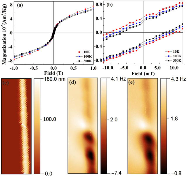
Figure 3. (a), (b) Magnetic properties of the as-grown Mn:CdS belts measured by SQUID. (a) The M–H curves of Mn:CdS belts at 10, 100 and 300 K. (b) The magnified area near the zero magnetic field of M–H curve near zero magnetic field. (c) Atomic force microscopy (AFM) topographic image of single Mn-doped CdS nanowire measured at 10 K and the corresponding magnetic force microscopy (MFM) image in constant height mode at 10 K (d) 20 nm and (e) 100 nm above the sample measured by a physical property measurement system (PPMS) cryostat using ATTO AFM/MFM Ixs, with the frequency shift of the cantilever (Budget sensor PPP magnetic tip) being the measurement parameter. The panel sizes of (c), (d), and (e) are 2 μm × 6 μm.
Download figure:
Standard image High-resolution imageMn2+ ions being actually embedded into the CdS matrix rather than lying at the distorted sites with independent phase (i.e., near the surface of belts) was proved by EPR measurements. EPR measurements were performed on the composite belts deposited on the silicon substrate (figure S5). An EPR spectrum with the well-defined six-equal-line pattern results from the hyperfine interaction of the unpaired electrons with Mn2+ nuclear spin (55Mn, I = 5/2). A six-line EPR spectrum also indicates that there is no direct bonding between Mn ions. The hyperfine splitting feature characteristic of Mn2+ ions with a hyperfine constant A of 68.9 Gauss is determined. This value is consistent with the earlier value reported, where Mn2+ ions are substituted at the tetrahedral Cd2+ cites in the CdS matrix [37, 38] and no direct bonds between Mn ions exist. However, six peaks appear, with unequal intensity and shapes, which cannot exclude the presence of neighboring Mn connecting via sulfur. If the doped ions were located close to or on the surface of the belts, they would prefer the octahedral coordination and bond less covalently than in the inner area of the belts [37]. As a result, the electron density will be higher in the Mn nucleus, which will produce larger hyperfine constant A. An asymmetrical profile as a whole, shown in figure S5, also indicated spin interactions between Mn ions, though it is a weak indication. Moreover, spatially inhomogeneous magnetic responses also reflected their multi-lifetimes in the belts.
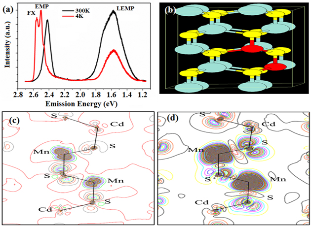
The semiconductor luminescence comes from their exciton recombination. In a DMS, the ferromagnetic order can bind with a free exciton to form the EMP. EMP emission may shift with the size of the DMS nanostructure as free exciton does. For a DMS QD, it cannot show independent EMP emission bands because most of DMSs QD cannot contain many TM ions or even form aggregates (need high temperature) to exhibit ferromagnetism. However, they can produce spontaneous magnetism after light excitation of EMP [39]. In bulk DMSs, EMP often comes out at low temperature considering its large physical space. Therefore, a close to micrometer-size of a DMS and low temperature are important for finding an EMP band accompanied by a free exciton band. They often combine with phonons to give band-edge emission of a DMS at room temperature. In our belt or wire, the EMP band clearly appears at the redside of the free exciton band with a decrease in temperature (start at about 180 K for sample with LEMP band at 760–780 nm), as shown in figure 4(a). Clearly, this EMP band appears through its ferromagnetization.
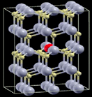
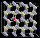
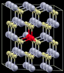
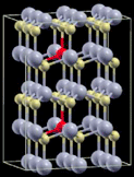
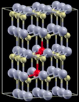
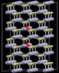
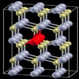
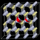
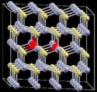
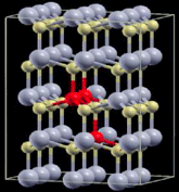
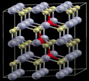
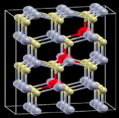
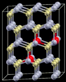
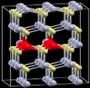
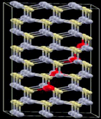
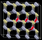
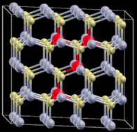
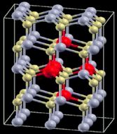
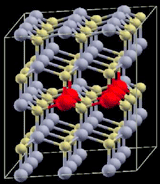
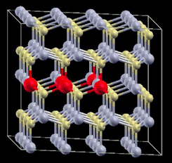
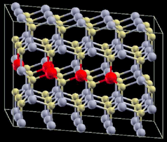
Figure 4. (a) Emission spectra of one CdS:Mn belt. (b) Unit cell of CdS:Mn. (c), (d) Spatial electronic density distribution of Mn–S–Mn clusters in a CdS lattice in the ground and excited states, respectively.
Download figure:
Standard image High-resolution image
The original assignment of lowest d-d radiation transition of Mn in CdS is 4T1–6A1. Because the Mn ion is in a high spin state, this transition undergoes a spin flip, as shown in the electronic levels in figure S6. The previously mentioned interactions between neighboring Mn sites after photoexcitation present like the Frenkel exciton interaction, which leads to a lower energy for their collective d-d transitions. The driving force for Frenkel exciton interaction in a conjugated molecule aggregate comes from the 1d dipolar orientation; however, d–d transition in a TM ion aggregate comes from its 3d spin exchange, because of the ferromagnetic coupling, not the antiferromagnetic coupling. This means that the bandgap reduction in these magnetic materials comes from the ferromagnetic coupling between spins, but not superexchange in the antiferromagnetic system. This description indicates that the d state and related d-d transition cannot be absolutely thought of as local within the Mn ion. Because of the presence of p-d hybridization, the electronic spatial distribution of the d state can extend to the nearest anionic and cationic ions (see figures 4(b)–(d)), which expand over three times of single Mn ion size by theoretical mimicking; the excited d state space is even larger than the ground state. So the concept of LEMP works well for the collective d-d transition in a ferromagnetic aggregate in this CdS crystal when several Mn ions moved to the nearest neighboring sites in this wurtzite structure, but not that the antiferromagnetic coupling in MnS crystal. Next, we studied the energy of such (MnS)n aggregates within a CdS lattice.
Based upon the preceding discussion, we can see that the EMP and LEMP in a DMS represent the optical excitations of spin–carrier interaction and spin–spin interaction, respectively, which coexist and indicate two different ferromagnetic origins. Although the ferromagnetism in DMSs has been studied for a long time, many models are presented; however, their relationship to their optical excitations still is not clear in the complicated material characters. Optical study on DMSs may facilitate further understanding of their quantum natures.
LEMP is used to describe the magnetic exciton on local d-d transition in a DMS [10, 11]. Two or more LEMPs occupying the nearest neighbor sites can interact to become a multiple LEMP (MLEMP based on aggregation degree); their energy can change upon change in the ion number, magnetic coupling, and ion configuration. By using the ab initio calculation technique, with consideration of p-d hybridization, presented in the Method section, the energies of different (MnS)n aggregates with different configurations and magnetic couplings are obtained as shown in table 1 (see supporting information method section for a detailed discussion of theoretical calculation method and description of table 1). Several interesting results are obtained. First, the aggregates out of antiferromagnetic coupling between Mn ions will have a transition energy higher than the lowest d-d transition at 575 nm—our emission bands in figure 2(a) all appear at its low energy side—so it could not originate from the antiferromagnetic aggregate in the CdS belt. Second, the ferromagnetic aggregates have energy values smaller than 575 nm, which accounts well for n increase from two to five; moreover, its energy also depends strongly upon the configuration of neighboring Mn ions. For n = 2,3,4, the energy values are discrete for the emissions close to 575 nm, whereas they may continuously change as n is over 5, because more configuration populations in the lattice broaden and shift the emission band. In this growth condition, they often exist in one belt (figure S7). The emission of an individual belt can be easily imaged using optical microscopy to show different colors (figure S8) and some images may be a mix of different wavelengths from one belt. Although there may be some defect states in the 600–900 nm range for as-prepared CdS belts, our calculations did not involve the contribution of defective effects. We cannot assign the tunable emission to structural defects here because of lifetime and calculation results. Therefore, we can assign these shifted emissions come from the ferromagnetic (MnS)n aggregates in CdS belt, and roughly the energy change ΔE (relative to the individual d-d lowest energy) increase with rising n value, like the quantum confinement effect for ferromagnetic cluster. This present us with a type of size effect for their optical and magnetic responses in a DMS and the aggregate size within CdS crystal determines their luminescence wavelength and magnetization. Local magnetization measurement is a big obstacle so far.
Table 1. The d–d transition energy of (MnS)n aggregates in CdS lattice with varied configurations.
| n | Mn2+-doped CdS 
|
Description of configuration | ΔE(d–d) (eV) | Wavelength (nm) |
|---|---|---|---|---|
| MnCd35S36(FM) | ||||
| 1 |
|
One Mn atom substitutes a Cd atom in a 3 × 3 × 2 supercell of CdS. | 2.1766 | 570 |
| MnCd63S64(FM) | ||||
| 2 |
|
4 × 4 × 2 supercell | −2.2329 | 555 |
| Mn2Cd34S36(FM) | ||||
| 3 |
|
3 × 3 × 2 supercell | 1.8857 | 658 |
| AFM | 2.1997 | 564 | ||
| Mn2Cd34S36(FM) | ||||
| 4 |
|
3 × 3 × 2 supercell | 2.0695 | 599 |
| AFM | 2.1765 | 570 | ||
| Mn2Cd34S36(FM) | ||||
| 5 |
|
3 × 3 × 2 supercell | 1.9299 | 643 |
| AFM | 2.1951 | 565 | ||
| Mn2Cd70S72(FM) | ||||
| 6 |
|
3 × 3 × 4 supercell | 1.655 | 749 |
| AFM | 1.6887 | 734 | ||
| Mn3Cd33S36(xy-60-FM) | ||||
| 7 |

|
3 × 3 × 2 supercell, three Mn atoms substitute Cd in an x–y plane and form a regular triangle (three angles are all 60°) | 1.7759 | 698 |
| Mn3Cd33S36(xy-120-FM) | ||||
| 8 |

|
3 × 3 × 2 supercell | 1.7679 | 701 |
| Mn3Cd33S36 (xy-180-FM) | ||||
| 9 |
|
3 × 3 × 2 supercell | 1.6772 | 739 |
| Mn3Cd61S64(xy-60-FM) | ||||
| 10 |
|
4 × 4 × 2 supercell, three Mn atoms substitute Cd in an x–y plane and form a regular triangle (three angles are all 60°) | 1.855 | 668 |
| Mn3Cd61S64(xy-120-FM) | ||||
| 11 |
|
4 × 4 × 2 supercell | 1.8384 | 675 |
| Mn3Cd61S64(xy-180-FM) | ||||
| 12 |

|
4 × 4 × 2 supercell | 1.8159 | 683 |
| Mn3Cd33S36(FM) | ||||
| 13 |
|
3 × 3 × 2 supercell | 1.7445 | 711 |
| Mn3Cd33S36(FM) | ||||
| 14 |
|
3 × 3 × 2 supercell | 1.7935 | 691 |
| Mn3Cd33S36 (zzz-p1-FM) | ||||
| 15 |

|
3 × 3 × 2 supercell | 1.8306 | 677 |
| Mn3Cd33S36 (zzz-p2-FM) | ||||
| 16 |
|
3 × 3 × 2 supercell | 1.9014 | 652 |
| Mn3Cd33S36 (zzz-p3-FM) | ||||
| 17 |
|
3 × 3 × 2 supercell | 1.7647 | 703 |
| Mn4Cd32S36(FM) | ||||
| 18 |

|
3 × 3 × 2 supercell | 1.6268 | 762 |
| AFM | 2.0433 | 607 | ||
| Mn4Cd32S36 (xy-diamond-FM) | ||||
| 19 |
|
3 × 3 × 2 supercell | 1.5813 | 784 |
| Mn4Cd68S72(FM) | ||||
| 20 |

|
3 × 3 × 4 supercell | 1.4649 | 846 |
| AFM | 1.6976 | 730 | ||
| Mn4Cd68S72(p1-FM) | ||||
| 21 |
|
3 × 3 × 2 supercell | 1.4953 | 829 |
| Mn4Cd44S48(Gamma-FM) | ||||
| 22 |
|
4 × 3 × 2 supercell | 1.6941 | 732 |
| Mn4Cd44S48 (7-FM) | ||||
| 23 |
|
4 × 3 × 2 supercell | 1.7431 | 711 |
| Mn4Cd36S40(xy-line-FM) | ||||
| 24 |

|
5 × 2 × 2 supercell | 1.6264 | 762 |
| Mn5Cd31S36(FM) | ||||
| 25 |

|
3 × 3 × 2 supercell | 1.4976 | 828 |
| Mn5Cd31S36(131-FM) | ||||
| 26 |
|
3 × 3 × 2 supercell | 1.5219 | 815 |
| Mn5Cd43S48(xy-2a3-60-FM) | ||||
| 27 |

|
4 × 3 × 2 supercell | 1.5433 | 803 |
| Mn5Cd43S48(xy-2a3-120-FM) | ||||
| 28 |
|
4 × 3 × 2 supercell | 1.5655 | 792 |
| Mn5Cd59S64(xy-11a3-60-FM) | ||||
| 29 |
|
4 × 4 × 2 supercell | 1.6331 | 759 |
| Mn5Cd59S64(xy-11a3-120-FM) | ||||
| 30 |

|
4 × 4 × 2 supercell | 1.6944 | 732 |
| Mn5Cd55S60(xy-2a3-z-FM) | ||||
| 31 |
|
5 × 3 × 2 supercell | 1.6897 | 734 |
| Mn5Cd43S48(xy-line-FM) | ||||
| 32 |

|
6 × 2 × 2 supercell | 1.5585 | 796 |
| Mn5Cd67S72(p-FM) | ||||
| 33 |

|
3 × 3 × 4 supercell | 1.4262 | 869 |
The preceding calculation is based on ferromagnetic coupling between neighboring Mn ions, but does not include the spin–carrier, spin–defect interactions; therefore, the calculated data have some errors compared with the experimental results. We see that ferromagnetic-coupled aggregates can account for the redshifted emission peaks or colors well (figure S8), whereas antiferromagnetic coupled aggregates cannot. The wavelength for the farthest emission peak detected can reach 1100 nm, which may be an aggregate of 8 Mn2+ ions. In the experiments, we found EMP emission enhancement and reduction of the LEMP band under a magnetic field. This example supplies a good platform to study the ferromagnetism of a DMS or at least to study a TM ion pair or aggregate that is certainly one origin of the ferromagnetism. Moreover, the ferromagnetic-coupled spins that are related to the individual luminescence bands in DMSs supply us with a new chance to study the ferromagnetism of a DMS with optical microscopy. The spin-related emission color cannot only be tuned by doping concentration; it can also be modulated by the magnetic field. This phenomenon is important for the fabrication of spin-polarized photonic devices.
4. Conclusions
In summary, high-quality 1D-Mn(II)-doped CdS belts with a varied concentration of Mn ions were synthesized using a CVD technique. The tunable emission band shifted from 570 to 850 nm and ferromagnetic responses were detected. These phenomena were related to the formation of the (MnS)n aggregate in the CdS matrix, as supported by the different characterizations, such as EDS, Raman, and EPR. The atomic diffusion movements in the micrometer-sized crystal matrix at high temperature are critical to forming such aggregates. Ab initio calculations on Mn-doped CdS crystals indicate that the tunable emission is caused by the formation of ferromagnetic aggregates of nearest neighbor Mn ions in tetrahedral symmetry, but not octahedral symmetry of bulk MnS crystal. Our findings may provide a novel way to produce luminescence material with tunable emission bands and a new experimental tool to study the origin of ferromagnetism and possible spin-related emissions in DMS nanostructures.
Acknowledgements
The authors thank the 973 Project (no. 2014CB920903) and NSFC project of China (no. 51002011 and no.11004009) for financial support.