Abstract
We have upgraded a low-temperature scanning tunnelling microscope (STM) with a radio-frequency (RF) modulation system to extend STM spectroscopy to the range of low energy excitations (<1 meV). We studied single molecules of a stable hydrocarbon π-radical weakly physisorbed on Au(111). At 5 K thermal excitation of the adsorbed molecules is inhibited due to the lack of short-wavelength phonons of the substrate. We demonstrate resonant excitation of mechanical modes of single molecules by RF tunnelling at 115 MHz, which induces structural changes in the molecule ranging from controlled diffusion and modification of bond angles to bond breaking as the ultimate climax (resonance catastrophe). Our results pave the way towards RF-STM-based spectroscopy and controlled manipulation of molecular nanostructures on a surface.
Export citation and abstract BibTeX RIS

Content from this work may be used under the terms of the Creative Commons Attribution 3.0 licence. Any further distribution of this work must maintain attribution to the author(s) and the title of the work, journal citation and DOI.
This article was amended on 23 September 2014 to correct the year in the published date.
Resonance phenomena are ubiquitous in nature, and man-made technology has extensively utilized them at macro- and microscopic length scales, like in musical instruments or the laser. Present nanoscience is aspiring an ever increasing spatio-temporal sensitivity in resonance experiments as impressively documented by the successful detection of the precession of an individual electron spin [1] or the motion of a single magnetic domain wall [2]. While recent years have witnessed technological improvements of home-built radio-frequency (RF) scanning tunnelling microscope (STM) systems [3], respective studies in the literature have been mostly limited to 'passive' noise spectroscopy [1, 4–6]. A next step has been taken by Loth et al by demonstrating an STM-based pulsed pump–probe experiment on a single atom at the nano-second timescale [7]. However, an 'active' RF-STM resonance experiment, i.e. with a periodic external stimulus tuned in resonance with a single quantum object, still remains to be demonstrated. The importance of such an experiment for the progress of STM-based single-molecule spectroscopy may be compared to that of magnetic resonance spectroscopy on macroscopic samples.
Here we report on the successful operation of an RF-STM at 5–7 K (figure 1(a)) that enables resonant excitation of single molecules by an external RF signal supplied through the tip. To substantiate the feasibility of active RF-STM spectroscopy, we applied the technique to the stable π radical α, γ-bisdiphenylene- -phenylallyl (BDPA) weakly physisorbed on the Au(111) surface [6, 8]. Resonant RF excitation of single BDPA molecules reveals an ac tunnelling channel at a frequency f = 115 MHz evidenced by an increase of the conductance, dI/dV . Moreover, it enables excitation of mechanical modes of BDPA/Au(111), which are inaccessible for thermal activation due to a lack of suitable substrate phonons at 5 K, allowing controlled modification of bond angles and even bond breaking between molecules (resonance catastrophe).
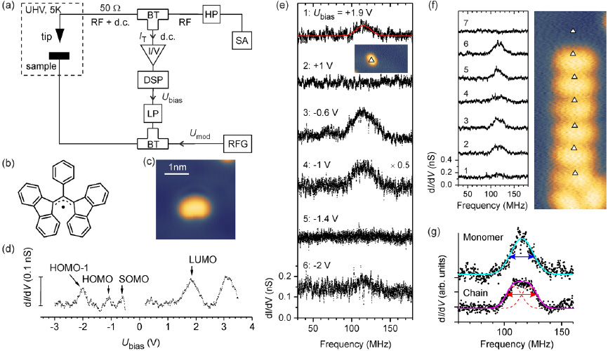
Figure 1. Tunnelling conductance resonance in a single molecule induced by RF modulation of bias voltage. (a) Schematics of the RF-STM experimental setup, including I/V conversion and amplification (gain 108, <7 kHz), low-pass and high-pass filters (LP, HP), bias-tee (BT) spectrum analyser (SA), RF-signal generator (RFG), digital signal processing unit (DSP), and bias-tees for separating dc and RF components of the tunnelling current signal. (b) Chemical structure of BDPA. (c) STM topographic image (+1 V, 50 pA) of a single BDPA molecule on Au(111). (d) Tunnelling conductance (dI/dV ) spectrum of BDPA/Au(111) after subtraction of the Au background signal; constant current of 0.2 nA; arrows mark energies of dI/dV peaks related to the highest occupied (HOMO), singly occupied (SOMO) and lowest (doubly) unoccupied (LUMO) molecular orbitals of BDPA. (e) Dependence of the RF-stimulated conductance resonance of a single BDPA monomer on the sample bias, Ubias; recorded at constant 0.2 nA tunnelling current, 5 K sample temperature, −20 dBm RF power, and 5 MHz s−1 sweep rate; RF frequency is swept from 30 to 180 MHz; multiple curves have been vertically offset for better clarity; solid line: numerical fit by single Gaussian function; inset: STM image of a single BDPA monomer; triangle marks position of STM tip. (f) RF-induced dI/dV resonance along a one-dimensional network of BDPA monomers recorded at +1.8 V and 5 K; tip positions for acquiring the spectra 1–7 are marked by triangles in the STM topographic inset (+1 V, 50 pA). (g) Comparison of RF-induced dI/dV resonance spectra of BDPA monomers (top) and one-dimensional chains (bottom); spectra have been vertically offset for better clarity; black dots: averaged data of 3 (9) independent measurements; curves: numerical fits of Gaussian functions; arrows mark the full width at half maximum of the dI/dV peak.
Download figure:
Standard image High-resolution imageBDPA is a non-polar and stable π radical that interacts only weakly with the Au(111) surface [8]. Figure 1(b) shows its chemical structure and figure 1(c) displays a topographic STM image of a single BDPA monomer adsorbed on a single-crystal Au(111) surface. The latter was prepared by repeated cycles of 0.6 keV Ar+ ion bombardment and annealing at 700 K. BDPA was thermally evaporated at ultra-high vacuum conditions from a quartz crucible at 370 K after thorough degassing. STM experiments were performed after in situ transfer of the sample, employing electrochemically etched W tips deoxidized by annealing in vacuum. Impurity- and tip effects were minimized by multiple tip formings between the experiments, resulting in a Au-coated STM tip. The differential tunnelling conductance, dI/dV , signal was obtained from the first-harmonic current signal detected by lock-in technique with sinusoidal modulation of the sample bias at 704 Hz and 20 mV peak-to-peak. Reliable tip performance was established by accurately reproducing the characteristic conductance signature of the Au(111) surface state well-known from the literature [9].
For the RF resonance experiments the STM tip is placed at a fixed lateral position of the sample. In addition to conventional dc tunnelling, a sinusoidal ac tunnelling voltage from an RF generator (Rohde & Schwarz, SMA 100A) is coupled-in via a bias-tee to the sample (figure 1(a)). The radio frequency is 3–4 orders of magnitude larger than, both, the cut-off frequency of the STM feedback-loop and the bandwidth of the high-gain current amplifier of the STM. Therefore, the resulting RF current does not affect the tunnel distance. The RF power level at the sample was set between −24 and −15 dBm monitored with a spectrum analyser (Agilent MXA 9020) connected at the tip side (figure 1(a)) and taking into account the damping of the RF circuit (see figure S1 available at stacks.iop.org/Nano/25/135705/mmedia). The STM is operated with active feedback-loop at constant-current condition, in order to compensate possible heating effects (STM drift) and piezo creep due to the supply of RF power and, moreover, to avoid mechanical (point) contact between tip and sample during the experiment. Figure S2 (available at stacks.iop.org/Nano/25/135705/mmedia) confirms that the dc tunnelling current over pure Au(111) is unaffected by the application of an RF modulation between 20 and 180 MHz. In the case of no RF modulation (conventional dc tunnelling) and fixed bias voltage the differential tunnelling conductance is constant. For instance, figure 1(d) yields a value of dI/dV ≈ 1 × 10⁻¹⁰ S for tunnelling at +1.9 V and 0.2 nA involving the lowest unoccupied molecular orbital (LUMO) of BDPA [8].
In the case of applying an external RF modulation at frequency f (ac tunnelling), however, we observe that dI/dV is no longer constant. It exhibits an intriguing dependence on the radio frequency, for tunnelling through the BDPA molecule at specific fixed bias voltages. At a fixed bias voltage of +1.9 V, while sweeping f, the conductance changes between f = 100 and 130 MHz, resulting in a distinct peak (curve 1 in figure 1(e)). Repeating the experiment with different STM tips and different BDPA monomers reproduces the dI/dV peak independent of the adsorption site of BDPA and the sample temperature (between 5 and 35 K, see supplementary figure S3 available at stacks.iop.org/Nano/25/135705/mmedia). A numerical fit of the averaged data with a single Gaussian function yields a centre frequency of 115.3 ± 0.2 MHz and a full-width-at-half-maximum of 22.6 ± 0.6 MHz (red curve in figure 1(e)). The dc conductance at resonance (i.e. at 115 MHz) is about 50% higher compared to off-resonance conditions in curve 1. Using different STM tips, the peak height at resonance is found to depend only slightly on the tip condition (figure S3 available at stacks.iop.org/Nano/25/135705/mmedia). More importantly, the peak height decreases monotonically upon lowering the RF power. The lowest power threshold for observing the RF resonance peak is close to −24 dBm for a tunnelling set-point of +1.9 V and 0.2 nA.
Figure 1(e) shows the bias dependence of the RF-induced dI/dV peak. The bias-voltage values of +1.9, −0.6, −1, and −2 V correspond to electron energies with enhanced density of states of BDPA adsorbed on Au(111) due to tunnelling through the LUMO, the highest singly- and highest doubly occupied MO (SOMO and HOMO, respectively) as well as the HOMO-1 (see figure 1(d)) [8]. Whenever the bias voltage is set at a fixed value corresponding to an MO energy of BDPA/Au(111), a similar dI/dV peak is observed at 115 MHz. This is clearly seen by comparing the different conductance curves 1, 3, 4, and 6. In contrast, no dI/dV peak is observed in the curves 2 and 5 recorded at bias voltages of +1 and −1.4 V, where electron tunnelling proceeds only between STM tip and Au substrate, but not via molecular states of BDPA (figure 1(d)). The bias dependence of the RF-induced dI/dV peak evidences the dependence on electron flow (tunnelling) through molecular states of BDPA. This is corroborated by figure S4 (available at stacks.iop.org/Nano/25/135705/mmedia), where no peak is observed over molecular contaminations of the sample (curve 1), over the pure Au(111) substrate (curve 2, with STM tip operated more than 1.5 nm away from BDPA), and with zero RF power over BDPA (curve 3).
The above results indicate that the RF-induced dI/dV peak observed over single BDPA monomers at 115 MHz exhibits the characteristics of a resonance phenomenon. We attribute it to a resonant excitation in the adsorbed BDPA molecule stimulated by the external RF modulation of the tunnelling electrons. Excitation is achieved only for tunnelling through molecular states of BDPA, thus creating additional conductance channels as evidenced by an increase of the dI/dV signal (figure 1(e)).
A similar dI/dV peak is observed in the case of BDPA monomers that are part of self-aligned one-dimensional networks of multiple BDPA monomers on Au(111) denoted herein as 'chains' [8] (figure 1(f)). The peak position is independent of the chain length and monomer position within the chain (curves 1–6), affirming that the dI/dV peak is due to a monomer effect. No peak is observed when the tip is operated about 1 nm outside of BDPA (curve 7), showing that the resonant RF excitation is localized on the monomer. A detailed analysis of the spectra in figure 1(f) reveals a small splitting of the dI/dV peak by ≈10 MHz. The splitting is better visible in figure 1(g) that compares averaged spectra (dots) of chains and monomers. The different shapes and widths (see arrows) of the dI/dV peaks of monomer (single peak) and chain (double peak) are clearly discernible and further confirmed by numerical fitting of the data with one (monomer) and two (chain) Gaussian functions shown as solid curves. The small splitting may indicate a weak radical–radical interaction along the chain [6, 8].
In the following, we present experimental results on the effect of increasing the power of resonant RF excitation on single BDPA monomers. We demonstrate that the 115 MHz excitation is accompanied by excitation of motional degrees of freedom of BDPA monomers adsorbed on Au(111). In this context, it is crucial to distinguish the RF-induced molecular motion from random motion caused by inelastic processes by dc tunnelling electrons. In contrast to isolated monomers [8], experiments on BDPA chains allow such a discrimination, because the lateral positions of the monomers of a BDPA chain on Au(111) are found to be unaffected by dc STM measurements at 5 K and typical tunnel conditions (|Ubias| < 2 V and I < 1 nA).
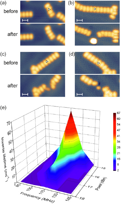
Figures 2(a)–(d) (top) show STM images of different BDPA chains on Au(111). After imaging the intact chain, the STM tip is placed over a single monomer of the chain (position marked by triangle) with active feedback-loop at a constant current of 0.2 nA and +1.9 V for tunnelling into the LUMO of BDPA/Au(111). Simultaneously, an RF stimulus is applied at 115 MHz in resonance with the BDPA monomer underneath the STM tip for a certain irradiation time, t, and power level, P. For a fixed value of 15 ≤ t ≤ 500 s we observe significant structural changes of the RF-excited BDPA (figures 2(a)–(d), bottom). In all chains studied, resonant RF excitation has induced a lateral translation of the BDPA monomer underneath the STM tip relative to the Au surface. The translation direction is approximately perpendicular to the chain axis. The total displacement of the RF-excited monomer of the BDPA chain shown in figure 2(a), bottom is only ∼0.2 nm, which leaves the chain intact. Above a certain threshold power level (see below) the displacement can exceed the length of a monomer, causing local breaking of the BDPA chains underneath the STM tip (figures 2(b)–(d), bottom). Chain breaking is often accompanied by an additional rotation of the displaced monomer (figure 2(c), bottom).
Figure 2. Structural modification and resonance catastrophe induced by resonant RF excitation of a monomer within one-dimensional chains of BDPA radicals on Au(111) at 5 K. ((a)–(d)) STM topographic images (+1 V, 50 pA) before and after application of a 115 MHz RF stimulus with STM tip over positions marked by the triangles; scale bar = 1 nm. (e) Inverse lifetime of BDPA molecular chains upon RF irradiation.
Download figure:
Standard image High-resolution image
The RF-induced breaking of a chain cluster is evidenced by considerable re-grouping of one or more individual monomers close to the position where the RF stimulus has been applied by the STM tip. Notice, that monomer motion is also indicated by a tiny flickering of the tunnelling current at resonance (figure S5 available at stacks.iop.org/Nano/25/135705/mmedia). In some cases, one or more monomers appear damaged (figure 2(c)) or are missing (figure 2(d)), possibly being dissociated, desorbed or picked up by the STM tip as a result of the resonant RF stimulus. Mechanical (point) contact between the STM tip and BDPA during chain breaking is ruled out by operating the STM at a constant current of 0.2 nA (compare figure S2 available at stacks.iop.org/Nano/25/135705/mmedia). Notice, that for point contact the (tunnelling) current is as high as I = Ubias ⋅ G0 ≈ 74 μA at Ubias = +1.9 V with G0 being the conductance quantum.
The chain-breaking effect is found to be current-dependent, with a low-current limit of approximately 50 pA, equivalent to three electrons per RF cycle. Furthermore, the effect is independent of chain length, sample temperature of 5–35 K, and monomer position within the chain. This confirms that the RF excitation occurs in a single BDPA monomer, consistent with the facts that coupling in the chains is weak and the excitation by the STM tip is local. Figure 2(e) summarizes the results of more than 60 independent RF resonance experiments on different BDPA chains and different combinations of t, P, and f. The chains are most affected at resonance, i.e. for f = 115 ± 12 MHz. In contrast, no effect is observed off-resonance, confirming that chain-excitation and chain-breaking effect is directly related to the RF excitation of the BDPA monomer. We attribute the chain-breaking effect to the phenomenon of 'resonance catastrophe', which is well-known in macroscopic mechanic systems [10], but previously unobserved in mechanic systems at the length scale of single molecules.
The observed coincidence of resonant RF excitation by STM and significant molecular motion of BDPA (figure 2) indicates a coupling between the two. The resonance frequency of f = 115 MHz suggests an excitation energy of hf = 0.5 μeV , which is three orders of magnitude smaller than the mean thermal energy of the substrate of 0.4 meV at 5 K. As confirmed by dc tunnelling, close to this temperature the 'thermal bath' of the Au surface is unable to induce the observed transverse motion of BDPA, which is, however, excitable by resonant RF excitation at 115 MHz via the STM tip. The thermal behaviour can be explained by the phonon spectrum of the reconstructed Au(111) surface. At energies of 0.4 meV and below it exhibits only phonons (bulk- as well as surface) close to the Γ-point [11], i.e. phonons with very large wavelengths compared to the size of a BDPA molecule. Thus, respective phonons are unable to induce the observed transverse deflections of BDPA on Au(111) or even achieve bond breaking. In addition, local heating effects by RF excitation of substrate phonons are ruled out as origin of the coupling by the same argument. We remark that dc tunnelling is not capable of inducing the observed chain breaking.
In the following we discuss possible physical phenomena behind the experimental results. Our experiments clearly evidence that ac tunnelling at radio frequencies enables the controlled excitation and manipulation of single BDPA molecules by STM at resonant conditions. The results evidence excitations based on the flow of electrons through a single molecule and therefore an electric-field effect of the STM tip is unlikely. The periodic flow of electrons (ac tunnelling) through the molecule may cause a periodic charging/discharging of the BDPA molecule under the tip. In general, different charge states of a molecule relate to different geometric equilibrium configurations of the molecular backbone, which are typically adopted on the pico-second timescale of molecular vibrations. The periodic structural changes caused by the ac tunnelling current may induce mechanical motion of BDPA relative to the substrate. Lateral motion of BDPA relative to the substrate is governed by weak attractive bonding interactions (intermolecular attraction in chains and monomer diffusion energy) [8], for which the estimated lower energy limit is on the order of 10 meV. Since this value is still several orders of magnitude larger than hf, it seems unlikely that hf corresponds to the energy of a mechanical mode of the adsorbed BDPA monomer. Instead, the resonance frequency may relate to a characteristic timescale of 1/f ∼ 8.7 ns reflecting the (nonradiative) decay time of the molecular ion to the neutral ground state. Similar decay times have been reported for molecular ions weakly physisorbed on a surface [12]. It is, however, unclear, how a timescale argument is able to explain the observed resonance behaviour (increased conductance; dI/dV peak). Alternatively, the small value of hf may point to a spin-related origin—in accordance with the pronounced Kondo effect of BDPA on Au(111) indicating preservation of its magnetic properties [6]. Supportively, surface contaminations that are most likely non-magnetic, exhibit no RF resonance behaviour in the experimental frequency range (figure S4 available at stacks.iop.org/Nano/25/135705/mmedia, curve 1). This scenario requires the RF tunnelling current to resonantly excite magnetic transitions between spin-split molecular levels as soon as the excitation energy (at 115 MHz) matches the spin splitting. Examples of possible types of spin-related phenomena are spin–orbit- and ligand field effects involving the Au substrate. On the other hand, the observed necessity of tunnelling through molecular orbitals suggests a coupling between the spin excitation and the periodic (de)population of a frontier molecular electronic level. Due to the radical nature of BDPA, for instance, populating the LUMO with an extra electron can either result in a singlet or triplet state in combination with the unpaired electron. RF-induced singlet/triplet transitions may induce a nonradiative decay to the ground state. The decay of the excited spin system may cause molecular motion through relaxation processes [13] similar to the well-known spin-lattice relaxation of magnetic materials. Here, the molecule itself acts as 'lattice', since the Au substrate lattice does not provide appropriate phonons (see above). In order to verify the different scenarios discussed (and eventually predict the resonance frequency) future experimental studies at different externally applied magnetic fields are required together with detailed electronic structure calculations including the electronic and magnetic molecule–substrate interactions.
In conclusion we have successfully demonstrated a novel RF-STM functionality that enables to resonantly excite a single quantum object by actively feeding-in an RF stimulus. Our STM results provide new insight into the resonance behaviour of a single molecule in the absence of thermal excitation and present first evidence on the excitation mechanism, which may trigger future theoretical modelling. The presented technique offers single-molecule sensitivity combined with excitation energies in the μeV -range with prospects for the study of a wealth of different quantum systems with resonance frequencies up to several GHz.
Acknowledgments
We thank A Ney and V Ney for fruitful discussions as well as Ch Diskus and R Rudersdorfer for helpful input on setting up our RF circuitry. We kindly acknowledge financial support of the projects P20773 and I958 by the Austrian Science Fund (FWF).