
Abstract
Metal nanoparticle solutions are widely used for the fabrication of printed electronic devices. The mechanical properties of the solution-processed metal nanoparticle thin films are very important for the robust and reliable operation of printed electronic devices. In this paper, we report the tensile characteristics of silver nanoparticle (Ag NP) thin films on flexible polymer substrates by observing the microstructures and measuring the electrical resistance under tensile strain. The effects of the annealing temperatures and periods of Ag NP thin films on their failure strains are explained with a microstructural investigation. The maximum failure strain for Ag NP thin film was 6.6% after initial sintering at 150 °C for 30 min. Thermal annealing at higher temperatures for longer periods resulted in a reduction of the maximum failure strain, presumably due to higher porosity and larger pore size. We also found that solution-processed Ag NP thin films have lower failure strains than those of electron beam evaporated Ag thin films due to their highly porous film morphologies.
Export citation and abstract BibTeX RIS
1. Introduction
Recently, there has been growing interest in various solution-based direct printing processes using metal nanoparticle-based inks such as gold (Au), silver (Ag) or copper (Cu) nanoparticles (NPs) with diameters ranging from a few to tens of nanometers for the fabrication of microelectronic devices. Representative printing methods are gravure printing [1, 2], flexography printing [2, 3], nanoimprinting [4–8], transfer patterning [9] and inkjet printing [10–15]. These technologies allow a simple fabrication process by means of all-solution processing without conventional deposition processes such as sputtering or evaporation, which require expensive equipment and tightly restricted vacuum conditions. Also, they have many advantages such as low energy consumption, a low manufacturing cost, and broad substrate compatibility. For these reasons, direct printing methods are widely used to manufacture micro/nano-scale metal electrodes and interconnections in electronic devices.
Many previous studies of printed metal NP thin films and micropatterns focused on changes in the microstructure and electrical conductivity by different thermal annealing conditions [12–17]. However, the mechanical characteristics of metal NP thin films fabricated by all-solution processes are very important because these devices often work under mechanical stresses caused by tension, bending and twisting, especially when the substrate is flexible. There have been some studies for measuring the mechanical properties, such as the elastic modulus and indentation hardness of Ag NP thin film [18], the stiffness and elastic modulus of a free-standing gold nanoparticle membrane by the nanoindentation method [19] and the strain sensitivity of gold nanoparticle film by tension tests [20]. In other research, it was demonstrated that both the elastic modulus and fatigue strength of Ag NP thin films can be improved through the formation of a composite film with carbon nanotubes (CNTs) [21]. However, research on the stretchability of solution-processed NP thin films and comparisons with metal thin films fabricated by vacuum deposition processes has not been conducted thus far to the best of the authors' knowledge. In addition, it is necessary to investigate the effects of the annealing temperature and period on the stretchability of metal NP thin films for the mechanically reliable operation of flexible electronic devices made of solution-processed metal NP thin films.
In this paper, we present the tensile failure behavior of Ag NP thin films coated on the flexible polyimide substrates given the formation and growth of cracks under increasing amounts of tensile strain. The effects of changing the grain structures of Ag NPs through the use of different annealing temperatures and periods on the tensile behavior of thin film are explained. Also, the failure strains of solution-processed Ag NP thin films are compared with those of electron beam (e-beam) evaporated Ag thin films.
2. Experiment
A flexible polymer (polyimide) substrate with a thickness of 25 μm was scribed using a cutting plotter (CE2000-120, Graphtec, Japan) for the specimen used in the tensile test. The shape of the specimen was a slender rectangle with a length of 28 mm and a width of 1 mm. The Ag NP solution (DGP 40LT-15C, Advanced Nano Products, Korea) was coated onto the scribed polyimide substrate using a coating bar (D-Bar, TND System, Korea). The Ag NP solution initially filled in the ∼10 μm deep grooves of the coating bar, after which it was coated onto the substrate along the moving direction. Afterwards, the Ag NP thin film was sintered in a convection oven at 150 °C for 30 min in order to remove any organic solvent and to form a conductive metallic film. The Ag NP thin film samples were then annealed in a convection oven at different temperatures (180 °C or 230 °C) for various periods (3, 6 and 9 h). This process resulted in Ag NP thin films with an average thickness of ∼500 nm regardless of the annealing temperature or period. As another set of samples, ∼400 nm thick Ag film was deposited on polyimide substrates by e-beam evaporation at a rate of 1–2 Å s−1 and was annealed at 150 °C or 220 °C for 2 h. After the annealing process of both solution-processed Ag NP thin films and e-beam evaporated Ag thin films, tensile tests were performed at a strain rate of 3.1 × 10⁻⁴ s−1 with a custom-made tensile tester with a displacement resolution of 10 μm, as shown in figures 1(a) and (b). Here, the strain rate was measured by the displacement of two grips which were fixed onto two tips of the sample. During the tensile test, the electrical resistance was measured in situ using a Keithley 2000 multimeter with a four-point measurement setup. The surface morphologies and microstructures of the Ag thin films were observed with a scanning electron microscope (SEM). The area ratio of the pores and the pore size (i.e. the pore diameter) on the surface of the Ag NP thin film were measured via the image processing of SEM photographs using ImageJ® software (National Institute of Health, USA) and Matrox Inspector® (Matrox, Canada), respectively.
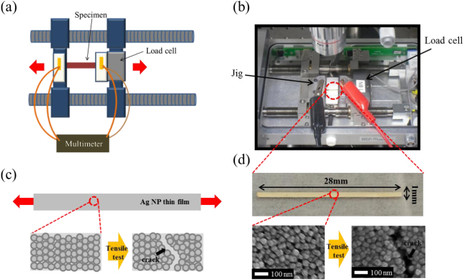
Figure 1. Tensile testing of solution-processed Ag NP thin films: (a) schematic diagram of the tensile equipment, (b) real photograph of the tensile equipment with the sample loaded, (c) schematic diagram of the specimen before and after the tensile test and (d) real photograph and SEM images of Ag NP thin film before and after the tensile test.
Download figure:
Standard image3. Results and discussions
A schematic and SEM images of crack propagation on the Ag NP thin film by tensile loading are shown in figures 1(c) and (d). A crack was formed perpendicular to the direction of tensile loading and propagated along the grain boundaries between Ag NPs. This phenomenon is consistent with previous studies of the crack propagation behavior in nanocrystalline metal thin films. In the work by Wang et al, the cracks which formed on a free-standing Au thin film were easily propagated along the grain boundary by an external tensile load [22]. Also, Farkas et al observed intergranular crack propagation in nanocrystalline nickel (Ni) by means of an atomistic computer simulation [23].
The surface morphologies and microstructures of Ag NP thin films annealed at different temperatures for various periods are shown in figure 2. After removing the solvent (methyl alcohol) of Ag NP ink and forming a solid thin film by an initial sintering process at 150 °C for 30 min, the Ag NP thin film showed a porous and granular structure with an average grain size of 25–30 nm. Further annealing at 180 °C resulted in the aggregation and grain growth of Ag NPs. At this temperature, the NP aggregation became more obvious as the annealing period was increased (3, 6 and 9 h). This phenomenon is usually caused by the decomposition of organic shells that were originally coated onto the surface of Ag NPs as a surfactant [13, 14]. However, when the Ag NP thin films were annealed at 230 °C, most NP aggregation and grain growth appeared to have occurred during the first three hours of annealing. At this temperature, no considerable changes in the microstructures (e.g. the grain size, porosity and pore size) arose after 6 and 9 h of annealing, as compared to the result at 3 h. Another notable fact is that Ag NP thin films annealed at 180 and 230 °C exhibited greater porosity, larger individual pores, and aggregation of the NPs compared to the initially sintered films (at 150 °C for 30 min). The area ratio of the pores of the initially sintered Ag NP thin film was only 2%. The area ratio of the pores was continuously increased by annealing at higher temperatures and for longer periods of time. Annealing at 230 °C for 9 h increased the porosity up to 5.2%, which is 2.6 times higher than that of the initially sintered Ag NP thin film. We found that the material of the organic shell surrounding Ag NPs is polyvinylpyrrolidone (PVP) by Fourier transform infrared spectroscopy (FTIR) analysis, as shown in figure S1 of the supplementary material (available at stacks.iop.org/Nano/24/085701/mmedia). The melting point of PVP is 150–180 °C. Therefore, organic shells began to decompose during the annealing process at temperatures higher than 150 °C. During the thermal annealing process, a close-packed structure of the individual NPs is broken but larger agglomerates are formed by the merging of NPs, increasing the size of individual pores. At the same time, the removal of organic shells results in the increase of porosity. Furthermore, a major difference in the thermal expansion coefficients of the polyimide substrate (αpolyimide = 55 × 10−6 °C−1) and the Ag NP thin film (αAg NP ∼ 1.9 × 10⁻⁶ °C−1 [18]) induced large thermal stress in the NP thin film during the thermal annealing process. As a result, larger pores and more initial cracks were generated on the Ag NP thin film by annealing at higher temperatures.

Figure 2. SEM images of surface morphologies of Ag NP thin films on flexible polyimide film after an annealing process at different temperatures for various periods of time.
Download figure:
Standard imageAssuming a constant electrical resistivity and Poisson ratio of 0.5 (i.e. no volume change by stress) during the deformation of the thin film, the ideal curve for the relative electrical resistance upon an increasing amount of tensile strain satisfies the following equation [24–27]

Here R is the electrical resistance of a thin metal film stretched to length L. R0 and L0 are respectively the initial resistance and length of the metal thin film. The failure strain was defined as the strain at which the measured resistance of a specimen deviated from the theoretical curve (1) by more than 5%. Previous studies [26, 27] verified that cracks typically start when there is a 5% deviation of the measured resistance from the theoretical curve. This phenomenon was also confirmed in this study. The initiation and growth of cracks result in an increase in the electrical resistivity, thus leading to a deviation from the theoretical curve based on the assumption of constant resistivity.
The resistance–elongation curves of Ag NP thin films annealed at 180 and 230 °C for 3, 6 and 9 h are shown in figures 3(a)–(c). The resistance–elongation curve for the initially sintered NP film has also been inserted into all of the figures for comparison. The failure strains of the Ag NP thin films are summarized in figure 3(d). The maximum failure strain was 6.6% (standard deviation (SD) = 0.3%) after initial sintering without an additional thermal annealing process at a higher temperature. On the other hand, the failure strains decreased to 4.6–5.4% and 3.8–4.9% after annealing at 180 °C and 230 °C, respectively. Although the statistical significance is low due to the large standard deviations, the general trend shows that the failure stains decrease by annealing at a higher temperature. It is generally known that the grains of metal thin films grow during the thermal annealing process [24]. In the present work, as shown in figure 2, Ag NPs did not grow continuously in proportion to the annealing periods during the annealing process at 230 °C. At this temperature, the grain growth appeared to be stabilized after 3 h of annealing. However, the connectivity between Ag NPs was continuously improved during the annealing process at 180 °C and 230 °C. These phenomena resulted in not only larger pore sizes but also larger area ratios of the pores (i.e. porosity) during the grain growth and aggregation of Ag NPs in the annealing process.
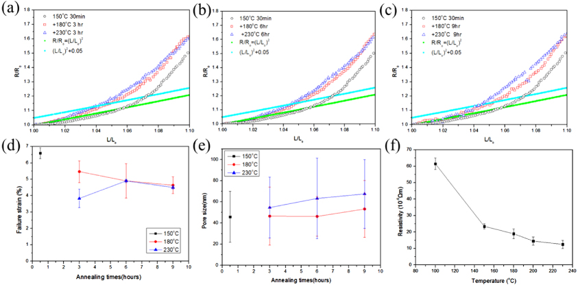
Figure 3. Resistance–elongation curves of Ag NP thin film on a polyimide substrate annealed at different temperatures (180 °C and 230 °C) for (a) 3 h, (b) 6 h and (c) 9 h. (d) Failure strains according to various annealing conditions, (e) pore size of annealed Ag NP thin films and (f) electrical resistivity of Ag NP thin films annealed at 100–230 °C for 1 h.
Download figure:
Standard imageFigure 3(e) shows the diameters of pores as measured by the image processing of the SEM photographs shown in figure 2. The average pore size was 45.9 nm (SD = 24.1 nm) for the specimen that was initially sintered at 150 °C for 30 min. For the specimens additionally annealed at 230 °C, the pore size increased to 54.6 nm (SD = 28.7 nm) after 3 h of annealing and to 67.5 nm (SD = 32.6 nm) after 9 h of annealing. The porosity and pore size of the thin film considerably affected the initiation and growth of cracks. In the work by Gerard et al, the authors demonstrated that crack initiation was observed adjacent to pores and that the pore-induced strain concentration accelerated the initiation of micro-cracks [28]. In the work by Lee et al, a lower surface porosity by oxygen-pressure-controlled annealing of a composite film composed of Ag NPs and carbon nanotube (CNT) resulted in a higher elastic modulus and yield strength compared to those of a composite film annealed under an ambient air condition [21]. Therefore, in the present work, larger pores and greater porosity could accelerate the initiation and growth of cracks, resulting in lower failure strains of Ag NP thin films annealed at higher temperatures. Also, the stress concentration factor increases with growing length of pore. The stress concentration factor is expressed as follows

In this equation, Kt,2a and ρ are the stress concentration factor, length of major axis of the pore and tip radius of the pore, respectively. In the present case, pores can be considered as pre-cracks. The Ag NP thin film annealed at higher temperature shows the increase of both the pore size 2a and tip radius ρ. However, the increase rate of the pore size is much higher than that of the tip radius. Therefore, the stress concentration factor Kt increases by annealing at higher temperature, causing an early failure under tensile stress (See figure S2 in the supplementary information available at stacks.iop.org/Nano/24/085701/mmedia).
Figure 3(f) shows the electrical resistivities of Ag NP thin film samples annealed at various temperatures (100–230 °C) for 1 h. After the annealing process at 100 °C without an initial sintering step, the resistivity was 6.15 × 10⁻⁷ Ω m (SD = 0.35 × 10⁻⁷ Ω m), which is 38 times higher than that of bulk silver (1.6 × 10⁻⁸ Ω m). This resulted from the incomplete removal of solvents and insufficient connections between Ag NPs in the film. However, the resistivity of Ag NP thin film decreased steeply to 2.35 × 10⁻⁷ Ω m (SD = 0.15 × 10⁻⁷ Ω m) after annealing at 150 °C. After annealing at 230 °C, the resistivity was measured as 1.25 × 10⁻⁷ Ω m (SD = 0.25 × 10⁻⁷ Ω m), which is only eight times higher than that of bulk Ag. This trend in the electrical conductivity with higher annealing temperatures is consistent with the findings in the literature [12–16]. However, as explained above, we found that the stretchability of Ag NP thin film degrades with higher annealing temperatures. An annealing process at a higher temperature could not improve both the electrical and mechanical tensile properties. In other words, the electrical properties can be improved by annealing at higher temperatures, but only with the sacrifice of mechanical stretchability.
The SEM images of Ag NP thin films annealed at various temperatures and stretched by 5% and 20% strains are shown in figure 4. As mentioned above, we found that the initially sintered Ag NP thin film has a failure strain of 6.6%. This is consistent with the SEM observation in which cracks were found not at ε = 5% but at ε = 20% (figure 4(a)). The failure strains for Ag NP thin films annealed at 180 °C and 230 °C for 3 h were 5.4% and 3.8%, respectively. The SEM images of these films show that small and short cracks were created after tension by 5% (figures 4(b) and (c)). The thin film annealed at 230 °C exhibits a higher number density and larger cracks than that annealed at 180 °C after extending by ε = 5%. This phenomenon is consistent with the fact that the failure strain is lower for the sample annealed at 230 °C (3.8%) than for the sample annealed at 180 °C (5.4%).
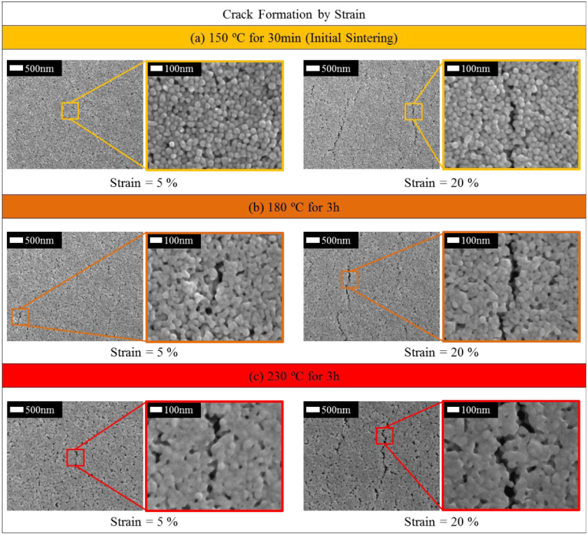
Figure 4. SEM images of cracks formed by tensile loading with 5% and 20% strain rates for Ag NP thin films annealed under various process conditions: ((a) 150 °C for 30 min, (b) 180 °C for 3 h and (c) 230 °C for 3 h).
Download figure:
Standard imageWe compared the failure strains of solution-processed Ag NP thin films with those of e-beam evaporated Ag thin films. The resistance–elongation curves and SEM images of surfaces of various specimens after tensile tests are shown in figure 5. The failure strains of e-beam evaporated films annealed at 150 °C and 220 °C for 2 h were 10% (SD = 1.8%) and 15.5% (SD = 0.9%), respectively, as shown in table 1. These values were about two–four times larger than those of the solution-processed and annealed Ag NP thin films. Also, the failure strains of the e-beam evaporated Ag films were improved by the annealing process at a higher temperature, as opposed to the solution-processed Ag NP thin films. As shown in figure 5(b), the surface morphology and microstructure of the e-beam evaporated Ag films were denser with larger grain size and fewer inter-grain pores than the solution-processed Ag NP thin films. These conditions resulted in mechanically robust metal films with higher failure strains. This shows that solution-processed Ag NP thin films are mechanically weaker with poorer stretchability than e-beam evaporated Ag thin films due to the significant difference in the microstructures.
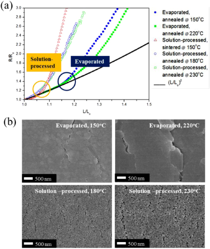
Figure 5. (a) The resistance–elongation curves of Ag NP thin film coated using a coating bar and Ag thin film deposited by electron beam evaporation. The failure strains for solution-processed Ag NP thin films and e-beam evaporated Ag thin films ranged from 3.8% to 6.6% and from 10% to 15.5%, respectively. (b) SEM images of cracks on the surface of tensile test specimens with 20% strain.
Download figure:
Standard imageTable 1. The failure strains of solution-processed Ag NP thin films and electron beam evaporated Ag thin films as annealed at the indicated temperatures and periods of time.
| Solution-processed Ag NP thin film | E-beam evaporated Ag thin film | ||||
|---|---|---|---|---|---|
| Annealing condition | Sintering (150 °C, 30 min) | 180 °C | 230 °C | 150 °C | 220 °C |
| (3 h) | (3 h) | (2 h) | (2 h) | ||
| Failure strain | 6.6% | 5.4% | 3.8% | 10% | 15.5% |
| (standard deviation) | (0.3%) | (0.7%) | (0.6%) | (1.8%) | (0.6%) |
In summary, we investigated the mechanical tensile characteristics of solution-processed Ag NP thin films on flexible polyimide substrates by observing the microstructures and measuring the electrical resistance under tensile strain. The effects of the annealing temperature and period on the microstructure and failure strain were investigated. A maximum failure strain of 6.6% was obtained from a specimen initially sintered at 150 °C, and the failure strains were reduced by additional annealing at higher temperatures and for longer periods of time. Although the electrical conductivity of Ag NP thin film was increased monotonically by annealing at higher temperatures, the stretchability of the film was worsened. Therefore, it is necessary to choose appropriate annealing temperatures and periods to achieve suitable levels of both electrical and mechanical properties of solution-processed Ag NP thin films. Ag NP thin films showed porous and granular microstructures as compared to e-beam evaporated Ag films with higher density and less porosity, resulting in lower failure strains than those of e-beam evaporated Ag films. It is believed that this work can provide a better understanding of the mechanical characteristics of solution-processed metal NP thin films under tensile loading for various electronics applications and that the results here can serve as a cornerstone for the design of fabrication processes of printed electronic devices with better mechanical reliability.
Acknowledgments
This research was supported by the Fundamental R&D Program for Core Technology of Materials funded by the Ministry of Knowledge Economy (K0006028) and by the Mid-career Research Program (Key Research) (2011-0027669) through the National Research Foundation of Korea (NRF) funded by the Korean government.