
Abstract
Resistive switching and conductance quantization are systematically studied in a Ag/poly(3-hexylthiophene):[6,6]-phenyl-C61-butyric acid methyl ester/indium–tin oxide sandwich structure. The observed bipolar switching behavior can be attributed to the formation and dissolution of Ag filaments during positive and negative voltage sweeps, respectively. More importantly, conductance quantization with both integer and half integer multiples of single atomic point contact can be realized by slowing down the voltage sweep speed as well as by pulse measurement. The former may reflect the formed Ag filaments with different atomic point contacts, while the latter probably originates from the interaction between the Ag filaments and the elemental hydrogen provided by the organic storage medium. With appropriate current compliances, low resistance states with desired quantized conductance values are successfully achieved, thus showing the potential for ultrahigh density memory applications. Besides, 100 successive switching cycles with densely distributed resistance values of each resistance state and extrapolated retention properties over ten years are also demonstrated.
Export citation and abstract BibTeX RIS
1. Introduction
Resistive random access memory (RRAM) has been attracting extensive attention mainly due to its non-volatility, fast speed, good endurance, and extremely high storage density, acting as one of the most promising candidates for future memory and logic circuit applications [1–4]. In particular, in the aspect of storage density, RRAM stands out in comparison with other candidates due to its simple metal–insulator–metal (MIM) structure, which enables it to be easily integrated in passive crossbar arrays with three-dimensional (3D) stacking structure. In this case, the cell area can be successfully reduced down to a minimum value of 4F2/m, where F is the minimum feature size and m is the number of stacking layers [3]. The feasibility of such a stacking structure has already been definitely demonstrated in a previous study [5]. To further increase storage density, achievement of multilevel operation in a single cell is highlighted, and a great deal of attention has been paid to this issue. In general, multilevel operation can be realized by precise control of either programming voltage or current compliance (CC), depending on the specific resistive switching character of the memory cell. For example, the former method is usually applied to memory cells with negative differential resistance behavior [6, 7], while the latter one is more appropriate for metallic filament-based memory cells [8, 9]. In order to avoid misreading errors, however, the number of levels is less than four in most cases owing to the wide distribution of resistance values in each level. Therefore, the search for a multilevel operation concept with a larger number of total levels is of great significance in performance enhancement of RRAM.
It is well known that a metallic filament-based RRAM generally consists of an insulator layer sandwiched between an electrochemically active metal electrode (usually Ag or Cu) and an inert metal electrode (e.g., Au or Pt). Under external voltages, the device can be reversibly modulated between a high resistance state (HRS) and a low resistance state (LRS), corresponding to the formation and dissolution of metallic filaments composed of the active metal atoms [10–14]. When the diameter of the metallic filament falls into the atomic scale, it is quite natural to expect that quantum size effects, such as conductance quantization, may take effect. If so, the conductance (G) in the LRS can be expressed as G = I/V = nG0 (n = 1,2,3,...), where I represents the current across the device under applied voltage V and G0 = 2e2/h (e is the electron charge and h is Planck's constant) refers to a single atomic point contact [15]. Apparently, the well-controlled conductance quantization exhibits great potential for ultrahigh density memory application. Indeed, the observation of conductance quantization has already been reported very recently in a few MIM structures with inorganic storage media, such as Nb/ZnO/Pt [16], Ag/Ta2O5/Pt [17], Ag/AgI/Pt [18], Ag/GeS2/W [19], etc. Compared with inorganic storage media, organic ones are undoubtedly more attractive given their easy as well as low-cost fabrication by spin-coating or ink-jet printing and their excellent flexibility in particular, showing wider application prospects in the future market for portable and smart electronic products [3, 5]. Consequently, it is increasingly meaningful to realize conduction quantization in RRAM with organic storage media. Here, we report conductance quantization during bipolar resistive switching in a Ag/poly(3-hexylthiophene):[6,6]-phenyl-C61-butyric acid methyl ester/indium–tin oxide (Ag/P3HT:PCBM/ITO in short) sandwich structure. By adopting appropriate CCs, conductance quantization with the desired values can be obtained. Moreover, the endurance and retention properties of the sandwich structure are also systematically characterized.
2. Experiments
The Ag/P3HT:PCBM/ITO devices were fabricated on ITO-coated glass substrates. First, the substrates were ultrasonically cleaned in acetone, ethanol and deionized water for a period of 8 min, respectively. Next, the P3HT:PCBM (Synwit Technology Co., Ltd) with a mass ratio of 1:0.8 was dissolved in dichlorobenzene with a total concentration of 27 mg ml−1. Subsequently, the solution was spin-coated on ITO substrates at 1000 rpm for 60 s. Finally, the Ag top electrodes with a diameter of 300 μm were deposited by direct current (DC) magnetron sputtering at room temperature by the use of a shadow mask.
The thickness of each layer in the sandwich structure was obtained by examining a cross-sectional specimen with a scanning electron microscope (SEM, LEO 1530). All the electrical properties were characterized on an Agilent B1500A semiconductor device analyzer in the atmospheric environment. All the bipolar resistive switching curves were recorded by the DC voltage sweep mode. The sweep speed was controlled by setting the increment of adjacent voltage steps with a constant duration of 20 ms for each step. For conventional bipolar resistive switching, the increments in the positive and negative voltage sweeps were 0.03 and 0.015 V, respectively. However, for the observation of conductance quantization, the increments in the positive and negative voltage sweeps were 0.005 and 0.003 V, respectively. For the pulse measurement, the interval and the increment of two adjacent pulses were fixed to be 2 s and 0.05 V, respectively. The widths of the positive and negative pulses were 1 μs and 5 ms, respectively. A basal voltage of 0.1 V was adopted to measure the conductance. In addition, to avoid fast degradation of device performance mainly due to the absorption of oxygen and water from the atmosphere, the devices were stored in a glove box (O2,H2O<1 ppm) filled with nitrogen apart from during the tests.
3. Results and discussion
The chemical structures of the P3HT and PCBM are displayed in figure 1(a). Figure 1(b) shows the device layout and measurement configuration. The external voltage is applied to the Ag top electrode with the ITO bottom electrode grounded all the time. A cross-sectional SEM image of the sandwich structure is illustrated in the inset of figure 1(b). According to the inset, the thicknesses of the Ag top electrode, the active organic layer and the ITO bottom electrode are about 100, 85 and 130 nm, respectively.
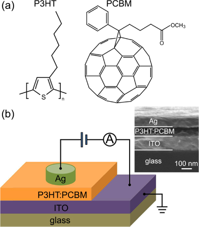
Figure 1. (a) Chemical structures of the P3HT and PCBM. (b) Schematic of the device layout and measurement configuration. The inset shows a cross-sectional SEM image of the sandwich structure.
Download figure:
Standard image High-resolution imageThe pristine device usually had a resistance value of ∼106 Ω. Successive bipolar resistive switching behavior can be observed after an electroforming process of ∼4 V, as shown by the red current–voltage (I–V) curve in figure 2. A CC of 1 mA was adopted to prevent permanent breakdown. By referring to previous studies on Cu/P3HT:PCBM/ITO [12] and Ag/P3HT/p+ poly-Si [14] sandwich structures, the observed switching phenomenon can be attributed to the Ag filaments resulting from the diffusion of Ag electrode metal into the organic layer. Thus, a complete Ag filament forms in the forming process, connecting the Ag top electrode and the ITO bottom electrode. The blue curve in figure 2 is a typical I–V curve of the bipolar resistive switching behavior. The reset process corresponds to electrochemical dissolution of the existing Ag filament, and the subsequent set process reconstructs the Ag filament on the residual Ag precipitate, resulting in the common phenomenon that the set voltage (∼1.1 V) is smaller than the electroforming voltage (∼4 V).
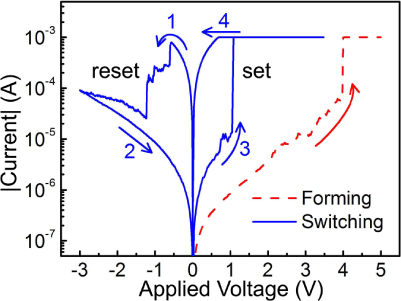
Figure 2. Typical I–V curves of the forming process (red) and bipolar resistive switching cycle (blue). The arrows denote voltage sweep directions.
Download figure:
Standard image High-resolution imageIf the increment of two adjacent voltage steps in the positive voltage sweep was reduced to 0.005 V, a multistep set process generally occurred instead of a sharp set process. The red curve in figure 3(a) is a typical I–V curve including three distinguishable current steps before reaching the CC of 500 μA. In an ascending order, the current values corresponding to each current step are ∼50, ∼100 and ∼150 μA, respectively. The multistep set process is reflected more clearly by the blue conductance–voltage (G–V) curve in the same figure. Note that the G–V curve is only given in the voltage region before the current reaches the CC, which is because the actual voltage applied to the device is out of control and consequently the conductance cannot be evaluated after the current reaches the CC [20]. Figure 3(b) is an enlarged view of the G–V curve in figure 3(a) with a voltage region from 0.4 to 1.0 V, demonstrating three stable quantized conductance plateaus during the set process. In detail, the conductance changes abruptly from the HRS to G0 at 0.52 V, followed by a plateau of 2G0. Similarly, a sudden increase of conductance from 2G0 to 3G0 is triggered at V = 0.77 V. The fact that quantized conductance plateaus always have integer multiples of G0 can in return serve as evidence for the existence of a Ag filament being responsible for the observed resistive switching behavior.

Figure 3. (a) I–V (red) and G–V (blue) curves of a typical multistep set process. The G–V curve with a voltage region from 0.4 to 1.0 V is magnified in (b). Quantized conductance plateaus of 1, 2 and 3G0 can be clearly seen. (c) Quantized conductance with desired values of 1, 2 and 3G0 can be realized by setting appropriate CCs of 50, 100 and 150 μA, respectively. (d) Resistive switching between the HRS and the desired quantized conductance. The insets in (c) and (d) are the corresponding conductance values in low voltage regions.
Download figure:
Standard image High-resolution imageHerein, it might be meaningful to explain why the conductance quantization is only observed during slow DC sweeps. From figure 3(b), we can see that each quantized conductance plateau lasts for a voltage region no larger than 0.1 V. The DC sweep speed in our experiment was controlled by setting the increment of adjacent voltage steps with a constant duration of 20 ms for each step. If the DC sweep is very fast, corresponding to a larger increment such as 0.03 V in figure 2, there will be no more than three measured data for each quantized conductance plateau. More frequently, there will be only a sharp transition from the HRS to the LRS without a multistep set process, as shown in figure 2. Under these circumstances, one can hardly identify the existence of any quantized conductance plateau. Therefore, slow speed is crucial to the observation of the conductance quantization in the DC voltage sweep mode.
Based on the stability of each quantized conductance plateau, one can spontaneously image the achievement of multilevel storage by taking advantage of the conductance quantization phenomenon. Indeed, quantized conductance in the memory cell with a desired value (such as G = G0) can be successfully obtained by adopting appropriate CCs during the set process, as demonstrated in figure 3(c). CCs of 50, 100 and 150 μA are chosen in accordance with the current steps in figure 3(a). The inset in figure 3(c) exhibits the corresponding G–V curves with a voltage region from 0 to 0.05 V, revealing evidently that quantized conductance with a desired value can be realized. In addition, resistive switching between the HRS and a stable quantized conductance state has been demonstrated (figure 3(d)), thus showing the potential for ultrahigh density memory applications.
On the basis of only the I–V and G–V curves in figure 3, one may argue that it is not convincing to declare that the quantized conductance behavior in our experiment originates from Ag filaments. In order to provide solid evidence for this point, two more experiments have been conducted. On the one hand, we plot the I–V curve of a device with a conductance of ∼1G0 in double logarithmic coordinates, as shown in figure 4(a). The fitted slope of ∼1.02 indicates that I is proportional to V and the conduction mechanism obeys Ohm's law. On the other hand, we have measured the I–V curves of a device with a conductance of ∼1G0 at various temperatures, as demonstrated in figure 4(b). According to this figure, one can see that the resistance of the device increases with increasing temperature, exhibiting a typical metallic behavior. All these experimental results strongly support the fact that the quantized conductance behavior in our experiment originates from Ag filaments. Furthermore, if the quantized conductance behavior originates from the regulation of the energy barrier for electronic carriers, the I–V curve will be highly non-linear in the same voltage region as that in figure 4(a) and the resistance will decrease with increasing temperature [21]; these are opposite to our experimental results.
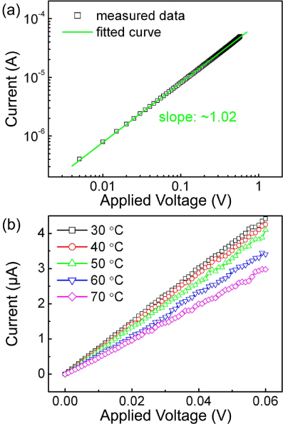
Figure 4. (a) I–V curve of a device with a conductance of ∼1G0 in double logarithmic coordinates. (b) I–V curves of a device with a conductance of ∼1G0 at various temperatures.
Download figure:
Standard image High-resolution imageSimilarly to the set process, conductance quantization could also be observed frequently during the reset process when the increment of two adjacent voltage steps in the negative voltage sweep was reduced to 0.003 V. Figure 5(a) shows the I–V and corresponding G–V curves of a typical reset process including six quantized conductance plateaus. In order to reflect the conductance quantization more clearly, the G–V curve in figure 5(a) with a voltage region from −1.8 to −1.0 V is enlarged in figure 5(b). The conductance is 7G0 at −1.0 V. With increasing amplitude of the negative voltage, four obvious conductance changes with a separation of 1G0 appear before the conductance stays at ∼3G0, each followed by a stable quantized conductance plateau. Then, conductance oscillations between 3G0 and 1G0 occur in the voltage range from −1.7 to −1.6 V, which is magnified in the inset of this figure. Conductance oscillations with integer multiples of G0 have also been reported in an ITO/ZnO/ITO sandwich structure [16], which are most likely caused by the competition between generation and rupture of nanoscale contacts inside the conducting filaments.
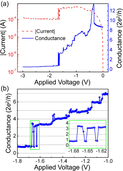
Figure 5. (a) I–V (red) and G–V (blue) curves of a typical multistep reset process. The G–V curve in the voltage region from −1.8 to −1.0 V is magnified in (b). Six stable quantized conductance plateaus can be observed. The inset shows the conductance oscillations between 3 and 1G0.
Download figure:
Standard image High-resolution imageIn addition to conductance quantization with integer multiples of G0, half integer conductance quantization has also sometimes been observed. Figure 6(a) shows a typical I–V of a set process with half integer conductance quantization. The G–V curve in figure 6(b) corresponds to the part of the I–V curve surrounded by the red rectangle in figure 6(a). Based on this curve, one can easily see the abrupt conductance change from 0.5G0 to 1.5G0, followed by a stable conductance plateau of 1.5G0. Analogously, a typical reset process including an abrupt conductance change from 1G0 to 0.5G0 is shown in figures 6(c) and (d). Furthermore, to make a statistical analysis of the conductance quantization phenomenon, more than 800 conductance values of stable conductance plateaus were extracted from about 150 set and reset processes. The histogram of these conductance values is shown in figure 6(e) and the red curve in this figure represents the Gaussian fitting. We can see that conductance peaks are located at both integer and half integer multiples of G0, with a small distribution around each peak. This result definitely indicates that conductance quantization can be realized in resistive memories with organic storage media. It is not in doubt that the conductance quantization with integer multiples of G0 originates from Ag filaments with different atomic point contacts. The conductance quantization with half integer multiples of G0, however, appears more frequently in our work than in work on resistive memories with inorganic storage media [16–19]. Previously, several studies have demonstrated that the occurrence of conductance quantization with half integer multiples of G0 can be induced by hydrogen adsorption on Au nanowires [22, 23]. In this work, the Ag filaments formed during set processes are closely surrounded by the organic storage medium, leading to possible interaction between the Ag filaments and the elemental hydrogen originating from the organic storage medium. In this case, it is reasonable that conductance quantization with half integer multiples of G0 appears more frequently in this study than in inorganic resistive memories.

Figure 6. I–V curves of typical set and reset processes with half integer quantized conductance are shown in (a) and (c), respectively. The regions surrounded by red rectangles in (a) and (c) are re-plotted in (b) and (d), respectively. (e) Histogram of more than 800 quantized conductance values extracted from about 150 set and reset processes. The Gaussian fitting curve serves as a guide to the eye.
Download figure:
Standard image High-resolution imageMoreover, conductance quantization can also be observed under pulse measurement. The interval and increment of two adjacent pulses were fixed to be 2 s and 0.05 V, respectively. A basal voltage of 0.1 V was adopted to measure the conductance. Figure 7(a) shows conductance quantization under positive voltage pulses with a width of 1 μs. Initially, the conductance is about 1G0. After a series of positive voltage pulses from 1.95 to 2.65 V, the conductance increases to 9G0. Figure 7(b) shows conductance quantization under negative voltage pulses with a width of 5 ms. The conductance decreases from 11G0 to 1.5G0 under a series of negative voltage pulses from −0.65 to −1.30 V. One can easily see that most of the stable conductance plateaus are located at integer or half integer multiples of G0, according well with figure 6(e).
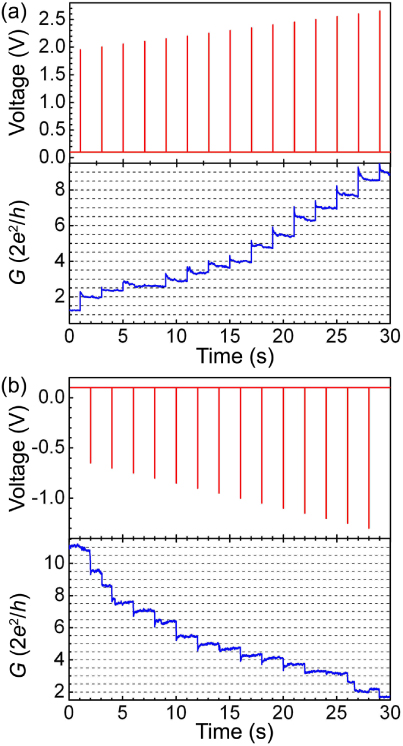
Figure 7. Conductance quantization observed under (a) positive voltage pulses with a width of 1 μs and (b) negative voltage pulses with a width of 5 ms. The interval and the increment of two adjacent pulses are 2 s and 0.05 V, respectively. A basal voltage of 0.1 V is adopted to measure the conductance.
Download figure:
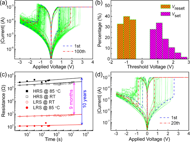
Standard image High-resolution imageFinally, as a memory device, it is important to investigate the statistical distribution of fundamental memory parameters, such as the resistance values of each state and the threshold voltages of the set as well as the reset processes. Figure 8(a) shows the I–V curves of 100 successive switching cycles obtained immediately after device fabrication. It is clear that the resistance values of the HRS and LRS are both densely distributed, thus providing a memory window larger than 20. The threshold voltages during these 100 successive switching cycles are also extracted and they are displayed by the histogram in figure 8(b). According to this histogram, Vset ranges from 0.5 to 2.9 V, while Vreset has an almost uniform distribution in a narrower region between −1.6 and −0.6 V. On the other hand, to evaluate the reliability of information storage, we carried out a retention test on both the HRS and the LRS at room temperature (RT) as well as at 85 ° C, as shown in figure 8(c). Each resistance state has negligible degradation up to 104 s at 85 ° C and nine months at RT, and it is expected that the resistance states could be maintained over ten years by extrapolating data. Moreover, our memory devices can still be successfully operated after storage for nine months, as demonstrated in figure 8(d), thus indicating good stability.
Figure 8. (a) I–V curves of 100 successive switching cycles obtained immediately after device fabrication. (b) Histogram of voltage thresholds extracted from the I–V curves in (a). (c) Retention properties of both the HRS and the LRS at RT as well as 85 ° C. (d) Switching characteristics of our memory devices after storage for nine months.
Download figure:
Standard image High-resolution image
4. Conclusions
In summary, we attribute the bipolar resistive switching phenomenon in a Ag/P3HT:PCBM/ITO sandwich structure to the formation and dissolution of Ag filaments during positive and negative voltage sweeps, respectively. By slowing down the voltage sweep speed or under pulse measurement, conductance quantization with both integer and half integer multiples of G0 has been observed. The former is caused by the formed Ag filaments with different atomic point contacts, while the latter probably originates from the interaction between the Ag filaments and the elemental hydrogen provided by the organic storage medium. More importantly, low resistance states with desired quantized conductance values of 1, 2 and 3G0 are successfully achieved with appropriate CCs of 50, 100, and 150 μA, respectively, thus showing the potential for ultrahigh density memory application. In addition, 100 successive switching cycles with densely distributed resistance values of each resistance state and extrapolated retention properties over ten years are also demonstrated.
Acknowledgments
This work was supported by the National Natural Science Foundation of China (Grant Nos 51231004 and 51202125), the National Basic Research Program of China (Grant No. 2010CB832905) and the National Hi-tech (R&D) Project of China (Grant No. 2012AA03A706).