
Abstract
We demonstrate strong electromagnetic field enhancement from nano-gaps embedded in silver gratings for visible wavelengths. These structures fabricated using a store-bought HD-DVD worth $10 and conventional micro-contact printing techniques have shown maximum fluorescence enhancement factors of up to 118 times when compared to a glass substrate under epi-fluorescent conditions. The novel fabrication procedure provides for the development of a cost-effective and facile plasmonic substrate for low-level chemical and biological detection. Electromagnetic field simulations were also performed that reveal the strong field confinement in the nano-gap region embedded in the silver grating, which is attributed to the combined effect of localized as well as propagating surface plasmons.
Export citation and abstract BibTeX RIS
1. Introduction
Surface plasmons have been used extensively in the past few decades for applications in sub-wavelength optics, data storage, optoelectronic circuits, diffraction-limited microscopy and bio-photonics. Recent years have seen a significant growth in the development of plasmonic nanostructures because of their ability to concentrate electromagnetic energy at sub-wavelength scales [1, 2]. The phenomenon of surface plasmon resonance (SPR) can enhance the interaction between the incident light and the metallic nanostructures, leading to highly localized electric fields within a few hundred nanometers [3, 4]. By confining light to volumes as small as 1 nm3, researchers have made optical wave guiding and imaging possible beyond the diffraction limit [5, 6]. Recent studies of novel metal nanostructures have unraveled a plethora of applications that utilize the near-field localization of light for signal enhancement [7, 8] as well as signal propagation [9]. Fluorescence spectroscopy, on the other hand, has emerged as one of the key techniques for performing basic research to clinical diagnostics and plays a key role in ultrasensitive chemical and biological threat sensors [10–12]. However, there has been a growing need to improve the contrast levels in fluorescence images and the limit of detection for fluorescence based sensing. The advent of plasmonics in recent years has provided some of the answers required to improve the quality of fluorescence microscopy and spectroscopy through surface patterning and novel geometries [13, 14]. The enhanced electromagnetic field produced by plasmonic nanostructures can be used to couple light to fluorescent dye molecules in the immediate environment, thereby providing the extreme signal amplification necessary for detecting trace quantities of biomolecules tagged with fluorophores [15]. Furthermore, the presence of nearby metallic films or nanoparticles has been known to profoundly affect the emission characteristics of fluorophores in terms of increasing the quantum yields of weakly fluorescent molecules, reduced lifetimes and subsequently improved photostabilities [16].
Propagating surface plasmons are charge oscillations present on a planar metal–dielectric interface with propagation lengths on the order of hundreds of microns [17–19]. A proficient way to couple propagating surface plasmons to incident light is through the use of metal gratings [20, 21]. These periodic structures provide additional optical momentum to the incoming incident light, necessary for exciting the surface plasmons [19]. The surface plasmon resonance angle θSPR, can be easily calculated theoretically from momentum matching conditions including the dispersion relationship in equation (1).

where ω is the angular frequency of the incident light, c is the speed of light in vacuum, εm is the dielectric constant for the metal, εd is the dielectric constant for the medium surrounding the metal, Λ is the grating pitch, kSP is the wavevector of the surface plasmon, and m is an integer. Equation (1) can be used to accurately predict the resonance angle for a periodic pattern in one-dimension. Both 1D and 2D metal grating structures have been fabricated and shown to provide considerable signal enhancements using epi-fluorescence microscopy [20, 22].
Metal nanoparticles and metallic nano-gaps on the other hand exhibit surface plasmons that are non-propagating in nature and are known as localized surface plasmons [23, 24]. Coupling an incident photon to such a nanostructure can be achieved by selecting the resonant wavelength, which depends on the shape, size, and dielectric environment of the metallic nano-gap. Metallic nano-gap bow-ties as well as bow-tie arrays have been fabricated using e-beam lithography and used to observe individual fluorescent molecules attached to the surface owing to extreme electromagnetic field enhancement within the bow-tie nano-gap region using confocal microscopy [16].
One can now envision a nanostructure that utilizes the combined effect of both the periodic metal gratings and the metallic nano-gap. In this case, the propagating surface plasmon polaritons (SPPs) travel as surface waves with high field intensity towards the metallic nano-gap, where the sudden field discontinuity causes 'extreme crowding' of the surface charges, leading to very high field intensities [25–30]. The field enhancement within the gap can be expected to be on the order of |εm/εd| owing to electromagnetic boundary conditions at the interface [31]. Hence, an individual nano-gap on a flat film will show a field enhancement of |εm/εd|, but a nano-gap embedded in a grating surface should show |εm/εd| times the electromagnetic enhancement due to the coupling of surface plasmon polaritons. However, it is also important to remember that this enhancement is dependent on the size and dimensions of the nano-gap itself. It has been shown experimentally and computationally that the field enhancement increases as the nano-gap width decreases [32, 33]. Since these structures combine both the localized surface plasmons (LPs) from the metallic nano-gaps as well as the SPPs from the metal gratings, the extreme field intensities can be used to excite fluorescent molecules in the vicinity, enabling the detection of very low concentrations of antibodies and proteins tagged with fluorophores, down to the single molecule level. Genevet et al exploited this idea and fabricated periodic arrays of nano-gaps and achieved up to 1000-fold field enhancements using a four-wave mixing setup [27].
Recent studies have shown the fabrication of sub-wavelength patterned metallic nanostructures using two-beam interference lithography, electron beam lithography and nano-imprint lithography [34] for enhanced fluorescence detection, microscopic imaging and surface enhance Raman spectroscopy (SERS) [16, 35, 36]. Although these techniques provide highly precise periodic structures and geometries on the nanoscale, they involve high cost and complexity in fabrication. Commercially available optical media on the other hand have drawn the attention of many researchers in the past few years as these offer an inexpensive alternative to fabrication of gratings [37, 38]. CDs, DVDs and other optical disks have periodic gratings in the form of tracks on the polycarbonate substrate that can be coated with metal films to form plasmonic metal gratings [39–41]. A disadvantage with this method, however, is that these polycarbonate surfaces have to be tuned to obtain sharp resonance peaks by chemical etching methods, which have issues with reliability and reproducibility.
In this work, we present a novel fabrication technique for producing polymethylsilsesquioxane (PMSSQ) based gratings embedded with nano-gaps using micro-contact printing [42, 43], where the starting master pattern is obtained from commercially available high-definition (HD) DVD-Rs. The nano-gaps occur spontaneously within the grating structure as a result of tensile strain in the elastomeric PDMS stamp during the printing process [44–46] (see supporting information for details available at stacks.iop.org/Nano/23/495201/mmedia). This method eliminates the high cost of production involved in conventional lithography and reactive ion-etching (RIE) procedures, providing substrates that are relatively fast, inexpensive and easy to fabricate. These nano-gap embedded PMSSQ gratings can be used as a base pattern for depositing metal layers for plasmonic nanostructures. We have produced nano-gap embedded silver gratings using this method for surface plasmon enhanced fluorescence and single molecule detection. Precise control of the nanofabrication of these structures can open doors to applications in diffraction-limited optics, optoelectronic circuits, and the observation of single molecule dynamics.
2. Materials and methods
For the fabrication process, polydimethylsiloxane (PDMS) μ-contact printing was used to stamp the nano-gap embedded gratings on glass substrates using a dilute PMSSQ based ink. A commercially available HD DVD-R was dissected into two parts to reveal the grating pattern on the inner side of the polycarbonate substrate. The substrate was cleaned using isopropanol to dissolve the dye coating layer covering the periodic pattern on the HD DVDs. The pattern was replicated using PDMS elastomer with a ratio of 5:1 for the PDMS base to the cross-linking agent (Sylgard® 184 silicone elastomer kit available through Dow Corning, Inc.). The grating pattern now being transferred to the PDMS was used as a stamp to print the pattern onto a glass substrate. The unique fabrication procedure utilizes a 3% by weight solution of PMSSQ (Techneglas Technical Products, GR-650F) in ethanol (Sigma Aldrich, 99%) as the 'ink' for the micro-contact printing process. PMSSQ was chosen as it is a cross-linking polymer that exhibits stability and robustness at room temperature. The ink was spin-coated on to the PDMS stamp at 3000 rpm for 30 s. The PDMS stamp was then printed on a silicon substrate and peeled off after 10 s using a pair of tweezers.
A very important by-product of this printing procedure is the formation of discontinuities or 'nano-gaps' in the PMSSQ gratings. The origin of these nano-gaps is believed to arise from the mechanical strain [45, 46] developed in the thin PMSSQ film (approximately 100 nm measured using ellipsometry) after the spin-coating step (figure 1). Even a slight bending of the elastomeric PDMS stamp produces a tensile strain in the thin PMSSQ film, which then leads to the formation [44] and transfer of the nano-gaps in the printing step, thereby producing nano-gap embedded grating structures. Since the fabrication procedure is done manually (by hand), we can expect a random distribution of the nano-gaps embedded in the gratings varying from stamp to stamp, depending on a myriad of factors such as the force with which the PDMS is peeled off, the direction of peeling as well as the extent of bending of the PDMS stamp [47]. However, the physics of the fluorescence enhancement arising from the resonant coupling of incident light with the evanescent field can be studied well from the random distribution of the nano-gaps in the grating structure.

Figure 1. (a) Spin-coated PMSSQ thin film on a PDMS stamp. (b) μ-contact printing on a glass or silicon substrate followed by peeling of the PDMS stamp using tweezers. (c) The formation of nano-gaps as a result of the tensile strain developed in the film during peel-off. A zoomed-in cross-sectional view of the fabricated nano-gap within the PMSSQ film is shown for clarity.
Download figure:
Standard imageFollowing the stamping procedure, the metal depositions were carried out using an AJA RF Magnetron sputtering system. The sputter process was carried out at room temperature, 100 W RF power, 20 sccm argon flow, and a deposition pressure of 4 mTorr. First, a 2 nm layer of titanium (0.2 Å s−1) was deposited on the substrate, which serves the purpose of giving better adhesion between the silicon and silver. Following this, a 100 nm layer of silver (100 W RF power, 4 mTorr argon pressure, 1.5 Å s−1 deposition rate) was deposited to complete the fabrication of the plasmonic substrates.
A commercial atomic force microscope—AFM 5500 system (Agilent Technologies) with a vista silicon tip (k = 40 N m−1,resonant frequency =∼295 kHz, length = 125 μm,width = 40 μm,tip height = 14 μm,tip radius ≤ 10 nm) was used to scan the fabricated samples in tapping mode. To image the nano-gaps embedded within the silver gratings, a Hitachi 4700 FE-SEM (field-emission scanning electron microscope) was used. Images were obtained using an accelerating voltage of 5000 V and an emission current of 11 000 nA. Reflectance measurements were performed using a J A Woollam variable angle spectroscopic ellipsometer (VASE). This setup consisted of a Xenon broadband source, which directed light through a monochromator via an optical fiber. To test the fluorescence enhancement from the fabricated nano-gap embedded silver gratings, a thin film of Rhodamine-doped PMSSQ in ethanol (10 μM) was deposited on top of the substrates using a spin-coater at 3000 rpm for 30 s [48]. The film thickness was determined to be 30 nm and the refractive index to be 1.41 using variable angle spectroscopic ellipsometry measurements.
3. Results and discussion
3.1. Surface characterization
The printed gratings after silver deposition were imaged using the above-mentioned conditions and showed a grating pitch of Λ = 401 ± 5 nm and a grating height of h = 64 ± 3 nm (figure 2).

Figure 2. (a) An atomic force micrograph showing the surface topography of the fabricated silver gratings. (b) Topography of the silver gratings measured using atomic force microscopy, showing a grating height of 65 nm.
Download figure:
Standard imageFigure 3 shows a top-view scanning electron micrograph of one of the nano-gaps cutting across the periodic silver grating and a lateral width of approximately 30 nm, which is not constant along the nano-gap length as it is a randomly formed nano-gap.

Figure 3. (a) A top-view SEM image of the nano-gap embedded in the silver gratings. (b) The two-point profile of the nano-gap along the yellow line shows a nano-gap with an approximate lateral width of 30 nm. (c) A three-dimensional SEM image taken for the nano-gaps cutting across the silver grating, taken at 5 keV accelerating voltage.
Download figure:
Standard image3.2. Optical characterization
Reflectance measurements are a standard way for spectral and angular characterization of plasmonic gratings [49, 50]. The fabricated silver gratings were characterized using a J A Woollam VASE with air as the surrounding medium. The light was then made incident on the silver grating sample with the gratings aligned perpendicular to the plane of incidence (as mentioned before) for optimum excitation of the surface plasmons on the silver grating. The proper alignment of the grating was made possible by cutting the PDMS stamps in such a fashion that the circular tracks on the HD-DVD were parallel to one of the edges. Since the direction of the circular tracks was known, the gratings were aligned perpendicular to the incoming light as they are parallel to the stamp edge. Only a transverse magnetic (TM) polarized electric field (x–z plane) with a component in the z-direction can generate surface plasmons, since the electron oscillations in this plane experience the discontinuity at z = 0. Suppose a transverse electric (TE) polarized electric field (x–y plane) was incident upon the interface, no surface plasmons would be generated since there is no discontinuity in this plane. Hence, surface plasmons modes can only be observed using TM polarization of the incident plane wave [19]. After reflecting from the silver grating substrate, the light reached the detector iris and was then passed on to a Si detector (spectral range: 200–1000 nm). The normalized reflectance curves as a function of the incident TM polarized wavelength from 500 to 700 nm (steps of 1 nm) for six different incident angles were obtained (figure 4). The resonance wavelength is characterized by a sharp minimum in the reflectance curves, indicating the localization of the electric field at the silver–air interface. Besides the sharp reflectance dip, which denotes the resonance wavelength for a specific angle of incidence, we observe a cusp that appears for slightly lower wavelengths, where the reflectance value drops as well. At the cusp, one of the diffracted orders has a diffraction angle of 90°, which leads to a lower value of reflectivity in that region [51]. The value of θSPR for 495 nm TM polarized light can be calculated to be 8° by linear extrapolation of the measured reflectance plots (figure 4 inset). This value agrees very well with the resonance angle calculated using equation (1). Similarly, the resonance angle for different wavelengths can be calculated from the linear fit obtained in figure 4.

Figure 4. Measured reflectance spectra for the fabricated silver gratings as a function of wavelength for six different incident angles: θinc = 15°, 20°, 25°, 30°, 35°, and 40°. The SPR angle (θSPR) is denoted by the sharp dip in reflected intensity at the minima. Inset: linear extrapolation of the measured data to calculate that θSPR = 8° for 495 nm transverse magnetic light.
Download figure:
Standard image3.3. Silver gratings FDTD simulations
It is imperative to realize the near-field electromagnetic distributions to compare the experimental results of fluorescence enhancement to electromagnetic field enhancement from the modeled simulations of the nano-gap embedded plasmonic gratings. For this purpose, electromagnetic field computations were performed using commercially purchased software—FullWAVE (RSoft Inc.) based on the finite difference time domain (FDTD) algorithm [52–54]. The first configuration used for field simulations was a silver grating with a semi-circular shape, a grating pitch of Λ = 400 nm, a grating height of h = 65 nm, and surrounding dielectric as air, which is very similar to the topography obtained using AFM. A rectangular launch field was described with unit power at z = 0.35 μm and the angle of incidence could be varied. A monitor was placed above the launch field at z = 0.38 μm, measuring the received power and averaging it over time to provide the final output. This monitor could be thought of as a detector that measures reflectance. The computational domain was defined from x =− 0.2 to +0.2 μm and z = 0 to 0.4 μm. A periodic boundary condition was used in the x-direction since the grating is periodic in this direction. For the maximum z value, a perfectly matched layer (PML) boundary condition was used, while the minimum z value used a perfect electric conductor (PEC) boundary condition, as this boundary is inside the silver surface and can be regarded as a perfect electrical conductor. The grid size was uniform and equal in both directions and chosen to be Δx = Δz = 0.005 μm. The FDTD stop time was set to 40 μm (in units of cT) and a continuous wave (CW) excitation was chosen to be incident upon the silver structure. The reflected power was detected using the monitor and plotted as a function of the angle of incidence (varying from 0° to 18°; steps of 0.01°) for an excitation wavelength of 495 nm and TM polarized light (E-field in the x–z plane). Figure 5 shows the reflectance as a function of the angle of incidence for the above simulation parameters. It is clear that, at an incidence angle of 8°, the reflectance drops to a minimum, which is characteristic of the SPR dip as seen in silver gratings. Hence, this structure simulates the fabricated samples very closely, as the silver plasmonic gratings also showed a θSPR = 8° for 495 nm TM polarized light in air, as shown previously.

Figure 5. Reflected power as measured by the monitor as a function of the angle of incidence. The SPR angle is denoted by the sharp dip in the reflectance value at 8° for 495 TM polarized light. This angle denotes the optimal coupling for the incident photons to the grating surface at a specific wavelength.
Download figure:
Standard imageTo map the near-field intensity distributions for the silver–air interface, another monitor was placed in the x–z plane; this measured the magnetic field going out of the plane (Hy) for the TM polarized 495 nm light. In figure 6, three different excitation angles are shown, and it is evident that the maximum field intensity ( ) is seen at θSPR = 8° as opposed to 0° or 18° incidence.

Figure 6. Field intensity distributions ( ) for three different angles of incidence with 495 nm TM polarized light. An angle of 8° provides the maximum field enhancement at the grating surface, while moving away from the SPR angle leads to lesser enhancement and a lower field concentration.
Download figure:
Standard imageThe field intensity was also plotted as a function of the distance into the dielectric (z) from the silver grating surface at x =− 0.1 μm (figure 7) and shows an evanescent profile for the SPR case. The maximum intensity is achieved at the silver–air interface and exponentially decreases as it moves into the air. The intensity reaches 1/e (37%) of its maximum value at a distance of  away from the interface, which is also known as the 'decay length'.

Figure 7. The field intensity as a function of the distance away from the metal–air interface, showing an exponential decay as expected for surface plasmon resonance and a  .
.
Download figure:
Standard imageBased on the field intensity obtained above and the quenching behavior of a metal surface, the optimal fluorophore placement can be chosen by taking these two competing phenomena into account. The emission efficiency (ηem) of the dye in this case is given by the following equation [55]:
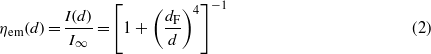
where d is the distance between the metal and the fluorophore, I(d) is the emission intensity at a finite distance d, dF is the Förster radius, and I∞ is the emission intensity where the fluorophore will not interact with the metal. The Förster radius is defined as the separation between the metal surface and the fluorophore where the emission efficiency is 0.5. Figure 8 shows the normalized field intensity of the evanescent surface plasmon on the silver gratings, the emission efficiency of a dye in the presence of a fluorophore (refer to equation (2)), and the product of both these curves. From this curve, one can see that the optimal fluorophore to grating distance, dopt, is 11 nm for a dye with Förster radius, dF = 5 nm.

Figure 8. (a) Normalized SPR intensity at resonance and fluorophore emission intensity as a function of the distance between the fluorophore and metal. The optimal separation is 11 nm for a Förster radius of 5 nm, and the maximum efficiency also decreases with increasing dopt, as shown in (b).
Download figure:
Standard imageThe optimal distance also changes as a function of the Förster radius and it can be seen that the maximum normalized intensity also decreases with increasing Förster radius [56, 57].
3.4. Nano-gap embedded silver gratings FDTD simulations
Since the nano-gap is of finite length, we cannot use the periodic boundary conditions anymore and will have to use PML in the x-direction. The new structure created is shown in figure 9, where the nano-gap with a lateral width of 20 nm (shown by SEM measurements previously) cuts across a silver grating structure with 21 periods. The computational domain was defined from x =− 4.2 to +4.2 μm (PML boundary condition at both boundaries), y = 0.03 μm (PEC) to 0.3 μm (PML), and z =− 2.5 to +2.5 μm (PML at both boundaries). The grid size for this three-dimensional computational domain was selected to be Δx = Δy = Δz = 0.01 μm. The FDTD stop time was set to 40 μm (in units of cT) and a continuous wave (CW) excitation was chosen to be incident upon this nanostructure.

Figure 9. Contour profile of the nano-gap embedded in silver gratings in three different planes.
Download figure:
Standard imageTo choose the number of periods necessary to get a plasmonic interaction from the designed configuration, a convergence study was performed by varying the number of periods, Np, from 1 to 29 (see supporting information available at stacks.iop.org/Nano/23/495201/mmedia). In the interest of keeping the computational domain smaller to avoid unrealistic simulation times, Np = 21 was chosen to be the optimal number to see the surface plasmon resonance from the silver gratings.
To see the field intensity distribution at the intersection of the nano-gap with the silver gratings, a spatial monitor was placed at y = 0.08 μm. The excitation conditions were chosen as 495 nm TM polarized light for an incidence angle of 8°, to achieve surface plasmon resonance on the silver gratings. For the same optical launch conditions, three different configurations (figure 9) were compared: a nano-gap with the gratings, the gratings without a nano-gap, and a nano-gap on a flat film. The intensity values obtained from the monitor placed at y = 0.08 μm, i.e., at the silver surface, for the different configurations in figure 10 are listed in table 1. The intensity values listed are for the point (0,0) in the field distribution maps. This demonstrates that the field enhancement in this case is due to the combined effect of grating coupled surface plasmon resonance (GC-SPR) and localized surface plasmon resonance, whereas in the case of silver gratings without nano-gaps the field enhancement is due only to the GC-SPR, and in the metallic nano-gap on a flat surface the enhancement is entirely due to a localized SPR phenomenon. The fluorescence enhancement characteristics of the nano-gap embedded gratings and their comparison to other plasmonic structures are discussed in section 3.5.

Figure 10. Field intensity distributions at the air–silver interface (top-view) for 495 nm TM polarized light (a) silver grating, (b) silver nano-gap and (c) nano-gap embedded in silver grating.
Download figure:
Standard imageTable 1. Field intensity values for the different configurations at point (0,0) under the same optical excitation conditions as shown in figure 10.
| Intensity | |
|---|---|
| Flat silver film | 1 |
| Nano-gap on flat silver | 3 |
| Silver grating | 52 |
| Nano-gap embedded in silver grating | 299 |
3.5. Fluorescence studies
Plasmonic gratings have been used extensively to excite the fluorophores present in the immediate vicinity of the evanescent field and achieve better limits of detection and improved imaging contrast in fluorescence microscopy [58, 59]. The combination of nano-gaps embedded in the plasmonic grating structure provides much higher levels of near-field concentration due to the combination of localized SPR and propagating surface plasmon polaritons, as discussed above. The evanescent field produced in the nano-gap embedded gratings is much stronger than the gratings alone. Therefore, we can expect much higher emission intensities from fluorophores present at the intersection of a nano-gap with the plasmonic grating, as opposed to a grating without the presence of nano-gaps or just nano-gaps on a flat silver film.
Fluorescence studies were performed using a traditional epi-fluorescence microscope setup in which light illuminates the sample in the form of a cone of excitation, which contains all angles from 0° to a maximum angle α, given by the following equation:

where NA is the numerical aperture of the objective lens used, n is the refractive index of the medium between the sample and the objective, and α is the maximum incident angle [60, 61]. For a 10 × objective lens with an NA of 0.3 and air surrounding the sample, the maximum incident angle is 17.5°, which is greater than the θSPR = 8° of the silver gratings in air for 495 nm light as shown previously via reflectance measurements. Hence, the surface plasmons on the silver gratings can be excited using just a regular microscope setup, as the θSPR is contained within the cone of excitation of a 10 × objective, which includes both TM as well as TE polarization states. Additionally, as seen in figure 11, the absorption peak of Rhodamine 6G (the dye used in this study) is centered on 535 nm and is ideal to be used with a fluorescein isothiocyanate (FITC) filter cube set, whose optical components are shown in the same figure.

Figure 11. The excitation and emission spectra of commercially available Rhodamine 590 (R6G) along with the optical components of the FITC filter cube set used for measuring fluorescence.
Download figure:
Standard imageThe plasmonic substrates after the fluorophore film deposition were imaged with an epi-fluorescence microscope (Olympus BX51WI) equipped with a 10 × objective (NA = 0.3), a FITC filter cube (excitation: 460–495 nm; emission: >516 nm), a 300 W Xenon broadband white light source, and a high-resolution detector (ORCA-Flash 2.8 CMOS Camera, Hamamatsu). The fluorescence micrograph shown in figure 12(a), obtained using a 10 × objective (NA = 0.3), displays a clear fluorescence enhancement at the nano-gaps when compared to the surrounding grating region.

Figure 12. Fluorescence micrographs of (a) 'nano-gaps' embedded in gratings, (b) 'nano-gaps' on flat silver and (c) glass slide taken with a 10 × objective and a FITC filter and a 6% ND filter and 60 ms exposure time of the CMOS detector. The intensity inside the nano-gap embedded gratings is much brighter than for nano-gaps on a flat film for the exact same fluorophore thin film on the surface.
Download figure:
Standard imageThe fluorescence enhancement factors (EF) for the different substrates with respect to bare glass slides were calculated using the following equation:
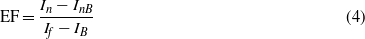
where In is the fluorescence intensity with the dye layer on the plasmonic substrate, InB is the intensity without the dye on the plasmonic substrate, and If and IB are the intensities with the dye and without the dye layers on glass, respectively. Fluorescence image analysis was performed using 'ImageJ' to measure the average and maximum intensity from the nano-gap regions. The performance of this substrate was evaluated by comparing the fluorescence intensities with other substrates, including nano-gaps on a flat silver surface, silver gratings with no nano-gaps, flat silver film and a transparent glass slide. As the quantum yield of Rhodamine 6G dye is inherently high (>95%), the fluorescence enhancements observed upon the plasmonic substrates may be attributed solely to enhanced absorption of the incident light due to the extreme field localization enabled by the substrate architecture. To reduce the intensity of the incident light on the samples to prevent photobleaching, a neutral density filter, U-25ND6 (6% transmission), was used.
Fluorescence data analysis was performed for the various micrographs obtained using the filter setup described above (see supporting information available at stacks.iop.org/Nano/23/495201/mmedia). Figure 13(a) shows the frequency distribution of the maximum enhancement factor, which is calculated using the highest pixel intensity within a nano-gap enclosed region in the fluorescence micrograph. Figure 13(b) shows the frequency distribution of the mean enhancement factor, which is calculated using the average pixel intensity within a nano-gap enclosed region in the fluorescence micrograph. The nano-gaps on flat silver films showed an average enhancement of 9 times when compared to a glass slide due to the excitation of localized surface plasmons [62]. The silver grating by itself provides almost a 25-fold enhancement factor when compared to glass. An average enhancement factor of 68 times (figure 13(d)) and a maximum enhancement of 118 times (figure 13(c)) was observed for the nano-gaps embedded in the gratings with respect to a microscope glass slide. It is evident that the nano-gap embedded gratings show a much higher enhancement than the nano-gaps on a flat silver surface that were prepared by using a flat PDMS stamp instead of a periodically patterned stamp. This effect can be attributed to the presence of propagating plasmons on the silver grating surface as opposed to no plasmonic coupling on the flat silver films. The combination of both the localized and propagating surface plasmons yields the maximum enhancement effect in this scenario.

Figure 13. Percentage distribution for (a) the maximum enhancement factor and (b) the mean enhancement factor for Rhodamine fluorescence in the case of nano-gaps embedded in silver gratings. Comparison of the fluorescence enhancement for different substrates with respect to a regular microscope glass slide for (c) maximum enhancement factor and (d) mean enhancement factor.
Download figure:
Standard imageThe nano-gap embedded gratings with the thin fluorophore layer were also imaged using SEM as well as an optical microscope for a bright-field image. Figure 14 shows the images of the exact same area imaged using three different techniques, which agree well with each other. The bright-field image shows the nano-gaps as dark features in a white background of the reflected silver gratings. The SEM image also provides leverage to the fact the extraordinary fluorescence enhancement seen in these samples is due to the presence of very narrow nano-gaps, which are on the order of 20–30 nm in terms of their lateral width.

Figure 14. (a) Fluorescence micrograph of the nano-gap embedded gratings with a thin Rhodamine-doped film on top using a 40 × objective and the FITC filter set. (b) Bright-field image of the exact same area using a 40 × objective. (c) SEM image of the same area as in (a) and (b) showing the actual physical dimensions of the nano-gaps.
Download figure:
Standard imageA 100 × oil-immersion objective (Olympus-UPlanApo, NA = 1.3) was also used to image the fluorescence from the nano-gap embedded silver gratings. Figure 15(a) shows a very high-resolution image depicting the silver gratings and the nano-gap cutting across them at a random angle. The points of extraordinary fluorescence intensity occur at the intersection of the nano-gap with the grating pattern, due to the extreme field enhancement at these points, which is expected from the FDTD simulation results shown earlier. The scanning electron micrograph of one of the ultra-fluorescent nano-gaps embedded in the silver grating pattern with the thin Rhodamine-doped film deposited on top (figure 15(b)) shows a nano-gap lateral width of approximately 20 nm.

Figure 15. (a) Fluorescence micrograph of the nano-gap embedded gratings with a thin Rhodamine-doped film on top using a 100 × oil-immersion objective and the FITC filter set. (b) SEM micrograph of the nano-gaps embedded in the gratings with the Rhodamine film on top, showing a lateral width of approximately 20 nm.
Download figure:
Standard imageFrom the fluorescence studies, it is evident that the nano-gaps embedded in gratings have much higher field intensities when compared to the gratings and the nano-gaps on a flat silver film under resonance conditions. However, these fluorescence enhancement factors are much lower compared to the field enhancement of 300 times observed using FDTD simulations for the nano-gap embedded gratings and field enhancement of 52 times for the silver gratings. This discrepancy comes from the fact that fluorescence enhancement depends not only on the electric field enhancement due to the plasmonic structure resonance, but is also heavily dependent on the optical characteristics of the fluorophore in the vicinity of the metal surface. In this case of thin fluorophore films on a plasmonic grating surface around 30 nm thick, the first 10 nm of the dye film will experience considerable quenching [63, 64], where as the top 20 nm will see the full effect of the evanescent field enhancement, as shown in section 3.4. Other possible reasons for the disagreement between the simulated enhancement factors in section 3.4 and the measured enhancement factors are as follows: (i) light illuminates the samples in the form of a cone of light containing not only the resonance angle but also other angles, leading to the observation of an average enhanced effect, where as the theoretical enhancement factors are a result of specific illumination at the resonance angle of incidence. (ii) The use of p-polarized light in the simulations ensured optimal surface plasmon excitation, whereas the non-polarized light source used in the microscope contained a mixture of different polarizations and was unable to effectively couple the surface plasmons. A combination of the above mentioned phenomena are responsible for much lower emission intensities than the theoretically possible maximum intensities in the case of these plasmonic nanostructures. Similar observations have been reported by Cui et al [20] for microscopic observation of silver gratings coated with Cy5 dye, showing an optimum enhancement factor of 30 times when compared to a glass slide using an epi-fluorescence optical setup. It should also be noted that the fluorescence response on the flat silver film was about three times greater than on glass slides, which is greater than the mirror effect (two times enhancement). This shows that the enhancement of plasmonic excitation also occurs to some extent on a flat metal film due to surface roughness.
Conclusion
In conclusion, we have demonstrated extraordinary fluorescence enhancement from nano-gap embedded plasmonic substrates fabricated using an HD-DVD as a starting mold. The extreme field concentration in this case occurs at the nanoscale due to the interaction between localized and propagating surface plasmons. The nano-gap regions embedded in the gratings show much higher field enhancement than nano-gaps on a flat surface, thereby demonstrating the importance of these nanostructures. Theoretical simulations also reveal that the TM modes for these structures exhibit very high electromagnetic field intensities, up to a factor of almost 300. The fluorescence enhancement from these nanostructures was experimentally observed using a broadband light source, showing maximum enhancement of 118 times when compared to a microscope glass slide.
Acknowledgments
The authors would like to acknowledge support from the National Science Foundation grant number 1102070 and the Center for Micro/Nano Systems and Nanotechnology at the University of Missouri, Columbia.