
Abstract
Here, a facile approach for the fabrication of CuS nanoparticle (NP)/ZnO nanowire (NW) heterostructures on a mesh substrate through a simple two-step solution method is demonstrated. Successive ionic layer adsorption and reaction (SILAR) was employed to uniformly deposit CuS NPs on the hydrothermally grown ZnO NW array. The synthesized CuS/ZnO heterostructure NWs exhibited superior photocatalytic activity under visible light compared to bare ZnO NWs. This strong photocatalytic activity under visible light is due to the interfacial charge transfer (IFCT) from the valence band of the ZnO NW to the CuS NP, which reduces CuS to Cu2S. After repeated cycles of photodecolorization of Acid Orange 7 (AO7), the photocatalytic behavior of CuS/ZnO heterostructure NWs exhibited no significant loss of activity. Furthermore, our CuS/ZnO NWs/mesh photocatalyst floats in solution via partial superhydrophobic modification of the NWs.
Export citation and abstract BibTeX RIS
1. Introduction
Zinc oxide (ZnO) nanomaterials have been studied extensively as photocatalysts due to their high surface area and high photosensitivity [1–4]. However, owing to its relatively wide bandgap (3.37 eV), a drawback of using ZnO in photocatalysis is that it can be activated mainly under UV light of wavelengths below 385 nm. UV light, however, accounts for less than 5% of the solar light energy reaching the Earth's surface and thus greatly restricts the practical application of ZnO photocatalysts. Modifying ZnO with noble metals, such as Pt [5, 6], Au [7, 8] and Ag [9], which work as electron traps, can improve its photocatalytic property by aiding electron–hole separation via the formation of a Schottky barrier at metal–semiconductor interfaces. However, the noble metals are expensive and rare. Therefore, numerous efforts have been undertaken to replace the noble metals with low cost cocatalysts. One of the widely used strategies to replace the noble metal and to extend the photoresponse of a wide bandgap semiconductor towards the visible spectral region is combining wide bandgap semiconductors with those with narrow bandgaps, such as CdSe [10], CdS [11–13] and PbS [14, 15]. Compared with a single semiconductor, composite semiconductors can extend the absorption range and enhance the absorption of the solar spectrum [16, 17]. However, the toxicity and harmful effects of cadmium, lead and their compounds to the environment and to human beings have caused them to be regulated by several regulatory control agencies. Hence, it is imperative to replace highly toxic cadmium or lead-based materials with other environmentally friendly ones.
For this reason, various non-toxic materials have been investigated; among them, copper sulfide has become one of the alternative candidates in modifying wide bandgap semiconductors because it is eco-friendly and economic [17–19]. Very recently, Gong et al [20] reported the fabrication of CuS/ZnS porous nanosheets and their visible-light-driven photocatalytic H2 production activity without having Pt as a cocatalyst. Liu et al [21] synthesized monodisperse CuS/ZnS hollow spheres and evaluated the photocatalytic decolorization of a Rhodamine B (RhB) aqueous solution under visible light irradiation. Both materials were proven to be efficient visible-light-driven photocatalysts. To the best of our knowledge, however, there is no report regarding CuS/ZnO heterostructure nanomaterial as an efficient visible-light-activated photocatalyst.
Here, we demonstrate the fabrication of CuS nanoparticle (NP)/ZnO nanowire (NW) heterostructures by a two-step solution reaction. A facile successive ionic layer adsorption and reaction (SILAR) method was used to deposit CuS NPs on the hydrothermally grown ZnO NW array. The photocatalytic properties of CuS/ZnO heterostructure NWs were investigated under visible light irradiation, and they exhibited high activities and stabilities for the photodegradation of Acid Orange 7 (AO7) in an aqueous solution. Furthermore, superhydrophobic modification of this sample enabled the nanowire/mesh substrate to float in solution, which can facilitate selective decomposition of floating pollutants and recycle the immobilized NW photocatalyst.
2. Experimental details
2.1. Materials
Zinc nitrate hexahydrate (Zn(NO3)2⋅6H2O, 98%), ammonium hydroxide (28 wt% NH3 in water, 99.99%), stearic acid (CH3(CH2)16COOH), copper(II) sulfate (CuSO4, 99.99%), sodium sulfide (Na2SO4, 98%) and Acid Orange 7 (4-(2-hydroxy-1-naphthylazo)benzenesulfonic acid, AO7) dye were purchased from Aldrich and used without further purification. Absolute ethanol was obtained from Fisher and used as received. Stainless steel mesh substrates were supplied from a general store. The water used in the experiment was prepared in a three-stage Millipore Milli-Q Plus purification system and had a resistivity higher than 18.2 MΩ cm.
2.2. Preparation of CuS/ZnO heterostructure nanowires
Well-aligned ZnO nanowire (NWs) arrays were grown on the mesh substrate using the ammonia solution hydrothermal method. First, 50 nm of ZnO seed layer was sputtered on the front and back side of the mesh substrate. The substrate was immersed into 10 mM of zinc ion solution prepared by dissolving Zn(NO3)2⋅6H2O into deionized water and adjusting to pH ∼11 and heated to 70 °C for 12 h. After the growth step, the substrate was washed by deionized water, gently dried by N2. CuS nanoparticle (NP)/ZnO NW heterostructure NW array was fabricated by the successive ionic layer adsorption and reaction (SILAR) method. The ZnO NW-coated substrate was immersed into the 50 mM Na2S aqueous solution and subsequently in the 25 mM CuSO4 aqueous solution at room temperature. After washing the substrate by deionized water and blowing by N2, CuS NPs were uniformly deposited on the ZnO NW.
2.3. Procedures of photocatalytic decomposition study
To examine the photocatalytic activity, Acid Orange 7 (AO7) was chosen as a probe molecule because of its resistance to biological degradation. The evaluation of the photocatalytic activity of the prepared samples for the photocatalytic decolorization of AO7 aqueous solution was performed at ambient temperature. Bare ZnO NW, CuS NP/ZnO NW sample cut into 2 cm × 2 cm were immersed into 50 ml of AO7 aqueous solution (1.0 × 10⁻⁵ M) and irradiated by a xenon lamp (300 W, Oriel, model 66902) directed towards the center of the sample in a closed system. A water filter mounted on the lamp housing to eliminate infrared radiation (IR) and a cutoff filter was placed outside the light slit of the lamp for the complete removal of radiation below 400 nm to ensure that photocatalysis is achieved by visible light irradiation only. Prior to irradiation, AO7 aqueous solution was vigorously stirred at room temperature and kept in the dark. After irradiation, the reaction solution was separated to measure the concentration change of the AO7. At regular irradiation time intervals, the dye remaining in solution was quantified by measuring the absorption intensity at 486 nm, which is the wavelength of maximum absorbance of AO7. The pH of the AO7 solution was ∼6 under our experimental conditions and the CuS/ZnO heterostructure nanowires were quite stable with no change in morphology even after photodecomposition experiments for two days.
2.4. Characterizations
The surface morphology of samples was characterized by field-emission scanning electron microscopy (FE-SEM, XL30S, Philips), and the detailed microscopic structure was observed by a high-resolution transmission electron microscope (HRTEM, JEM2010F, JEOL). The chemical composition and binding states of the samples were analyzed using x-ray photoelectron spectra (XPS, ESCALAB 220i-XL, Thermo VG) using monochromatic Mg Kα radiation as the x-ray source. Prior to data analysis, the binding energies were charge-corrected using the C–C component of the C 1s signal at 284.6 eV. The phase and the crystallinity of the samples were determined by x-ray powder diffraction (XRD, Max-2500 V, Rigaku). The light absorption spectra of degraded AO7 aqueous solution were recorded with a UV–vis spectrophotometer (Optizen POP, Mecasys Co., Ltd, Korea).
3. Results and discussion
The morphology of the ZnO NW arrays after the CuS NP deposition process was observed by FE-SEM, as shown in figure 1. Figure 1(a) shows the top view of the mesh substrate fully covered with vertically grown CuS/ZnO heterostructure NWs. A low-magnification image (figure 1(b)) shows that ZnO NW arrays were uniformly grown on both sides of the mesh substrate. The ZnO NWs have diameters of 50–100 nm and lengths of 3–4 µm, as confirmed by a higher magnification image shown in the inset of figure 1(b). After CuS NPs were deposited using SILAR, it was difficult to find significant changes in the diameters of the NWs, observe the aggregation of the NPs or surface roughening. However, the TEM image of CuS/ZnO heterostructure NWs in figure 1(c) clearly confirms that CuS NPs are uniformly dispersed on the ZnO NW. An HRTEM image of the CuS/ZnO heterojunction region (figure 1(d)) reveals that polycrystalline CuS NPs, with diameters below 5 nm, were deposited on the ZnO NW surface. Electron energy loss spectroscopy (EELS) mapping (figures 1(e)–(h)) clearly shows that Zn and O are uniformly distributed along the nanowire, while Cu and S elements are found on the same spots corresponding to the position of the nanoparticles. This result was also confirmed by the XRD results as shown in figure 2. X-ray diffraction peaks of CuS/ZnO heterostructure NWs can be indexed to the wurtzite phase of ZnO (JCPDS no. 76-0764) and the hexagonal phase of CuS (JCPDS no. 06-0464).
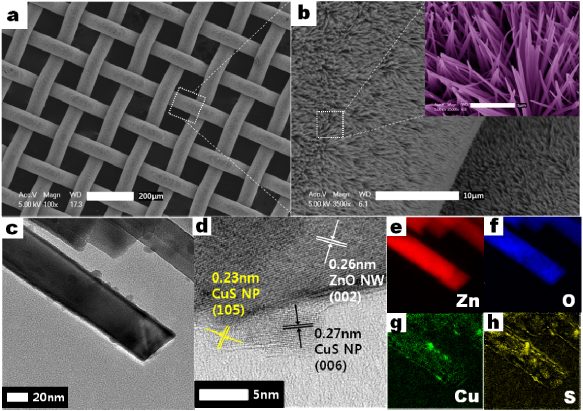
Figure 1. SEM images of (a) CuS/ZnO heterostructure nanowires grown on the stainless steel mesh substrate and (b) low magnification of the top-view image. The inset is a high-magnification top-view image of (b). TEM images of CuS/ZnO heterostructure nanowires: (c) a low-magnification image and (d) a high-resolution TEM (HRTEM) image. (e)–(h) EELS elemental mapping images of the Zn, O, Cu and S, respectively.
Download figure:
Standard image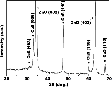
Figure 2. X-ray diffraction (XRD) patterns of CuS/ZnO heterostructure nanowires.
Download figure:
Standard image
The optical absorbances of bare ZnO NWs and CuS/ZnO heterostructure NWs were measured by UV–vis diffuse reflectance spectra (DRS) at room temperature, as shown in figure 3. CuS/ZnO heterostructure NWs were prepared using various SILAR cycle numbers from 1 to 10 SILAR cycles. The absorption edge value of ZnO NWs was obtained at 380 nm (3.27 eV), which coincides with the reported values in the literature [22, 23]. In comparison with the ZnO NWs, all of the CuS/ZnO heterostructure NWs clearly exhibited an optical response in the visible light range, especially the 400–550 nm and 700–800 nm wavelength regions. The absorption edges of the CuS/ZnO heterostructure NWs shifted towards a longer wavelength region with increasing CuS content. This absorption band at 400–550 nm can be assigned to the direct interfacial charge transfer (IFCT) from the VB of ZnO to CuS [24–29]. The additional absorption in the range of 700–800 nm is due to the d–d transition of Cu2+ [26–30].
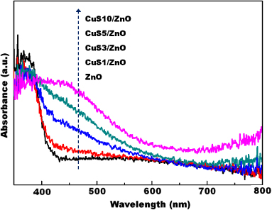
Figure 3. UV–vis diffuse reflection spectra of CuS/ZnO heterostructure nanowires plotted at various SILAR deposition cycles of CuS.
Download figure:
Standard imageTo investigate the chemical binding states of the CuS/ZnO heterostructure NWs, the XPS analysis was performed. The chemical states of Cu were determined from Cu 2p peaks. Figure 4 shows the comparison between the XPS spectra of Cu 2p for the as-prepared CuS/ZnO heterostructure NWs and the NWs after 2 h of visible light irradiation. For the as-prepared CuS/ZnO heterostructures, two main peaks were observed at 932.8 and 952.8 eV and were assigned to Cu 2p3/2 and Cu 2p1/2, respectively. These peaks were accompanied by weak shake-up satellite peaks at approximately 943 eV, which is indicative of the presence of the paramagnetic chemical state of Cu2+ [31, 32]. After 2 h of visible light irradiation, the satellite disappeared and the binding energies of Cu 2p1/2 and Cu 2p3/2 shifted. The disappearance of the Cu 2p satellite, which is a fingerprint of Cu2+, was monitored and no satellite features indicated the presence of either Cu0 or Cu+ species rather than Cu2+. However, the evidence was corroborated by the associated Auger line (Cu LMM) at 569.6 eV, which is the typical value for Cu2S [33, 34] and we suggest that Cu+ was generated under visible light irradiation. It is conceivable that the Cu2+ in CuS is reduced to Cu+ due to the photo-generated electron transfer from the VB of ZnO to CuS.
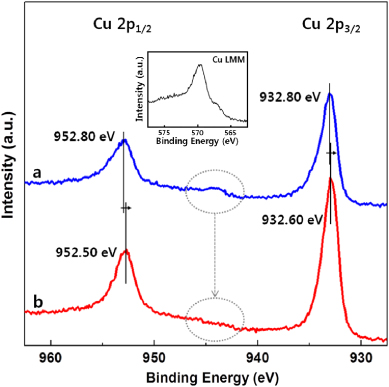
Figure 4. XPS spectra of Cu 2p of CuS/ZnO heterostructure nanowires: (a) as-prepared sample and (b) sample treated with 2 h irradiation of visible light. The inset is the Auger Cu LMM lines of sample (b).
Download figure:
Standard imageBased on the observations and discussions above, the IFCT process in our CuS/ZnO NWs is proposed and illustrated in scheme 1. The band edge positions of the conduction band and valence band of ZnO can be determined by a simple approach [35, 36]. The bandgap of ZnO was found to be 3.27 eV based on the UV–vis results. The calculated conduction and valence band positions of ZnO are −0.86 and 2.42 eV, respectively, as shown in scheme 1. The potential of CuS/Cu2S is approximately −0.5 V (versus SHE, pH = 0) [20], and the interfacial transition energy from the VB of ZnO to CuS/Cu2S is determined to be 2.92 eV. Therefore, the idea that the absorption in the range of 400–550 nm causes the direct IFCT from the VB of ZnO to CuS is perfectly plausible based on the XPS results and the above explanation.
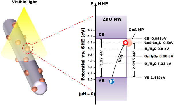
Scheme 1. Schematic illustration for the CuS/ZnO heterostructure nanowires and proposed interfacial charge transfer process from the valence band of ZnO NW to the CuS NP under visible light irradiation.
Download figure:
Standard imageThe photocatalytic degradation of aqueous solutions of AO7 in the presence of ZnO NWs and CuS/ZnO NWs under visible light irradiation is depicted in figure 5(a). In the absence of the catalyst, the concentration of the AO7 solution was almost constant during the irradiation of the solution. Bare ZnO NW photocatalysts showed negligible photocatalytic activity, which is due to the wide bandgap of ZnO and the lack of absorption in the visible region. CuS/ZnO heterostructure NWs showed greatly enhanced photocatalytic activity compared to that of the bare ZnO NWs. This remarkable increase in the photocatalytic activity of CuS/ZnO heterostructure NWs may be attributed to the catalytic activity of photoproduced reduction from CuS to Cu2S through IFCT from the VB of ZnO to CuS NP, as discussed above (scheme 1). Visible-light-initiated IFCT has been reported by other researchers. Very recently, Hashimoto et al reported that Cu(II)–TiO2 [30] and Cu(II)–WO3 [31] systems are sensitive to visible light by IFCT, as predicted by Hush [37–39] and theoretically formulated by Creutz et al [40, 41]. Electrons in the VB of semiconductors are directly transferred to Cu(II) and reduced to Cu(I). This IFCT in composite semiconductors, such as our CuS/ZnO NWs, plays an important role in charge separation and reducing recombination, which enhances the photocatalytic activity of composite photocatalysts.
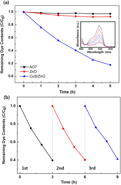
Figure 5. (a) Comparison of photocatalytic activities of bare ZnO nanowires and CuS/ZnO heterostructure nanowires for the photocatalytic decolorization of AO7 in water. The inset is absorption intensity changes of AO7 aqueous solution in the presence of CuS/ZnO heterostructure nanowires. (b) Cycling degradation curves for CuS/ZnO photocatalysts.
Download figure:
Standard imageDuring the irradiation of CuS/ZnO NWs, Cu2+ in CuS is reduced to Cu+ by transferred photoinduced electrons, and the produced Cu+ is converted back to Cu2+ when it reacts with adsorbed O2 dissolved in the aqueous AO7 solution through a multi-electron reduction process [42–45]. A generated hydroxyl radical (OH•) can decompose organic compounds [46]. The proposed mechanism of the photocatalytic decomposition of AO7 by CuS/ZnO heterostructure NWs can be described as follows:


The recycle experiments were conducted to evaluate the photostability of CuS/ZnO heterostructure NW photocatalysts. After each cycle, the CuS/ZnO NW photocatalyst was washed with DI water and the AO7 aqueous solution was refreshed with new solutions. As illustrated in figure 5(b), after three cycles of photodecolorization of AO7, the photocatalytic behavior of CuS/ZnO heterostructures exhibited no significant loss of activity. The recycle experiments indicate that the CuS/ZnO heterostructure photocatalyst is sufficiently stable and not deactivated during the photodegradation of the organic dye; thus, it has potentially practical applications in treating contaminated water.
Due to the inherent NW structure, the CuS/ZnO NWs/mesh substrate can float in solution through the chemical modification of the NWs as shown in figure 6. The fabrication of a superhydrophobic surface through the chemical modification of the NWs has been studied using various nanowire materials [47, 48]. After chemical modification with stearic acid (SA), CuS/ZnO heterostructure NWs grown on the mesh substrate could remain stable and float on the water, even though the density of the mesh is 8.03 g cm−3 (much greater than that of water). The typical contact angle of a water droplet on our heterostructure nanowires was ∼155°. Floatability of the photocatalyst is useful in selective decomposition of floating pollutants, such as oils and other low-density materials. Floatability also helps the recycling/reuse of the immobilized NW photocatalyst, which is quite difficult in the case of using suspensions of powdered materials.
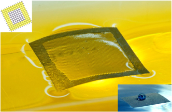
Figure 6. Photograph of stearic acid (SA)-treated CuS/ZnO heterostructure nanowires/mesh floating on the AO7 aqueous solution. Top left corner is a schematic illustration of mesh substrate with modified edge through chemical coating of SA. Bottom right corner is the photograph of SA-treated ZnO NWs grown on the mesh substrate floating on the water. The water droplet sits on top of the ZnO NWs, forming a spherical shape.
Download figure:
Standard image4. Conclusion
In summary, CuS/ZnO heterostructure NWs were synthesized by a simple two-step solution reaction. The prepared CuS/ZnO heterostructures can serve as an excellent photocatalyst under visible light irradiation. It is believed that the direct IFCT from the VB of ZnO to CuS plays an important role in charge separation and reducing recombination for high photocatalytic activity, which causes the reduction of CuS to Cu2S. CuS/ZnO heterostructure NWs are promising for industrial applications because of their remarkable photocatalytic stability and floating characteristics.
Acknowledgments
This work was supported by grants from the National Research Foundation (NRF2010-0009545 and NRF2010-0015975) and by the Korean Research Foundation Grants funded by the Korean Government (MOEHRD) (KRF-2008-005-J00501).