

Abstract
Accurate and traceable measurements of critical dimension (CD) and sidewall profile of extreme ultraviolet (EUV) photomask structures using atomic force microscopes (AFMs) are introduced in this paper. An instrument complementarily applied with two kinds of AFM techniques, the CD-AFM and the tilting-AFM, has been developed. High measurement stability of the instrument is demonstrated, for instance, the long-term CD stability is better than 1 nm over 500 successive measurements over 55 h. To traceably calibrate the effective tip geometry, transmission electron microscopes-based method is applied, which uses either the silicon crystal lattice or the structure pitch value calibrated by metrological AFMs as an internal scale. Several grating patterns with different nominal CDs and line/space ratios of an EUV photomask have been measured using the developed methods. A data evaluation method with considered higher order tip effect due to the non-vertical sidewall is introduced. Detailed measurement results of a test EUV photomask, such as middle CD, left and right sidewall angle, feature height, line edge roughness and edge profiles are given. Finally, the AFM results are compared to that of a PTB EUV scatterometer. The comparison of the middle CD yields a linear relation within a spread of only about ±2 nm and an offset of the absolute values below 3 nm. For the sidewall angle, both methods yield consistent results within a range of about 2°.
Export citation and abstract BibTeX RIS
1. Introduction
The reduction of feature sizes in the semiconductor industry is now approaching technology nodes below 22 nm. To further improve the capability of patterning smaller structures, research and development are exploiting conventional photolithography using, for instance, immersion lithography and double patterning techniques on the one hand and next-generation lithography techniques on the other hand. The latter covers a variety of methods like extreme ultraviolet lithography (EUV lithography), electron and focused ion beam lithography as well as nanoimprint lithography. Among them, EUV lithography is prominently in the research and development focus and prototype lithography tools are available today.
The photomask is a key component in lithography systems. During the lithography process, the structure patterns on the photomask will be transferred and demagnified by the ratio 4:1 to the silicon wafer by the imaging system of the lithography tools. The measurement of the structure pattern on the photomask is an important task, since its quality will directly impact that of end products. It is particularly important for the EUV photomask, where more complicated materials are applied in its fabrication. Besides the pattern displacement parameters such as overlay, the structure parameters, such as critical dimension (CD), sidewall angle, height and line edge roughness (LER), need to be measured accurately.
A number of techniques are available today in measuring the dimensional parameters of nanostructures, including optical microscopy, optical scatterometry [1, 2] with visible and shorter wavelengths (EUV, x-ray), CD scanning electron microscopy (CD-SEM) [3] and atomic force microscopy (AFM) [4]. Optical microscopy still plays an important role in submicron metrology due to its versatility, simplicity and speed. However, its resolution is limited by the diffracting nature of the light. Optical scatterometry analyses the diffraction pattern of the periodical structure to reveal information about its profile and has the advantages of optical techniques, i.e., it is fast, non-invasive and applicable for in situ measurements. Recently, it has been explored extensively for measuring nanostructures in the semiconductor industry. However, challenging issues remain, in particular in resolving the information about grating profile and dimensional parameters from the measured diffraction pattern, an issue known as the inverse problem of scatterometry. Such challenges include, for instance, the requirement of prior knowledge of the 3D geometry of the structures and the multiple minima (ambiguities) issue. CD-SEM is capable of imaging structures with a resolution of the primary electrons down to 1.5 nm and even below by using very low electron energies. However, CD-SEM uses the secondary electrons (SEs) generated within the sample surface as the measurement signal; it is a kind of 2D measurement technique and must be operated in vacuum. In addition, to achieve accurate and optimum results in CD metrology, prior knowledge of the 3D geometry of the structures is also necessary for SEM to interpret the SE edge bloom. Furthermore, the charging and contamination issues of SEM still remain challenging today. AFM allows direct and nearly non-destructive measurements of the 3D shape of nanostructures with both high lateral and vertical resolution. Compared to other methods, it is the least model and material dependent one due to its relatively straightforward measurement principle. However, AFM measurements are usually slow. The image is the dilated result of the real structure by the tip geometry, consequently tip issues, for instance the tip geometry, tip wear and tip–sample interaction, become challenging issues for AFM metrology too.
In this paper, we introduce the measurement of an EUV photomask using two different AFM techniques: CD-AFM and tilting-AFM. The instrument development, its typical measurement performance, the realization of the traceability and detailed measurement results of a test EUV photomask are introduced. Finally, the AFM results are compared with those of an EUV scatterometer, showing very promising agreement.
2. Instruments
2.1. Principle
Two different AFM techniques, CD-AFM and tilting-AFM, have been applied to measure the EUV photomask. CD-AFM uses flared tips. Such tips have an extended geometry near their free end which enables the probing of steep and even undercut sidewalls, as shown in figure 1(a). The CD-AFM technique has advantages of measuring both the left and right sidewalls of nanostructures in only one measurement. However, it has disadvantages, such as the relatively large tip geometry (typically tens to hundreds of nanometres), which limits its spatial resolution for measuring very dense structure patterns, and the complicated tip shape, which makes the tip characterization more difficult.

Figure 1. Principle of CD-AFM (a) and tilting-AFM (b) applied in the measurement.
Download figure:
Standard image High-resolution imageTo extend the measurement capability of CD-AFM the tilting-AFM technique has been developed and implemented recently. The advantage of tilting-AFM lies in its capability of applying very fine conical tips, for instance, super sharp silicon tips with a radius down to 2 nm, which offer better capability for measurement of dense structure patterns as well as for the corner rounding and footing of structures. But the tilting-AFM has its own limitations too. In order to make the sidewalls of steep structures measurable, the AFM tip has to be tilted with respect to the structure by a certain angle, as shown in figure 1(b). As only one side of the structure is measurable at one tilted setup, either the AFM tip or the sample must be rotated so that the opposite side of the structure becomes measurable. Consequently, the images obtained at different tilting views must be stitched together to determine the CD, where the stitching error will strongly influence the measurement accuracy.
In this study, we apply both techniques in a complementary manner, adding their strengths and overcoming their limitations, and thus reducing the measurement uncertainty and expanding the metrology versatility.
Both techniques are realized in a self-made AFM at PTB. The realization of the CD-AFM has been introduced in detail elsewhere [5], therefore, only a brief introduction is given here. The AFM uses the classic optical lever technique to detect the bending and torsion of the cantilever. The AFM measurements are mostly performed in the intermittent-contact mode, where the amplitude modulation technique is applied for detecting the tip–sample interaction. For achieving better CD measurement performance, new probing and measurement strategies have been developed [5]. The tilting-AFM is an add-on function of the existing instrument, by applying a new type of AFM tip and manually tilting the scanner (together with the AFM head), while all other components including the controller and software are kept the same. The tilting angle is currently about 11° in the tilting-AFM setup.
The AFM is based on a scanning head design. This affords the advantage that large samples such as wafers and photomasks can be held stationary while the tip is scanned during measurements. A commercial six-axis nano positioning stage (type P-561K034, Physik Instrumente GmbH) is applied for moving the AFM head. The nano positioning stage is a flexure hinge stage driven by piezo actuators and its positions and angles are measured and servo-controlled using high-resolution capacitive sensors. The displacement scaling factors of the AFM scanner are traceably calibrated using a set of step height and lateral standards that were measured by the PTB metrological large-range AFM [8] having a relative calibration uncertainty of about 0.1%. Since most structures being measured at the CD-AFM have a line width of several hundreds of nanometres only, the corresponding uncertainty component is a minor contribution to the overall uncertainty budget of the instrument for CD metrology.
The measurement range of the AFM is 15 µm ×45 µm × 45 µm (x, y and z). An air bearing stage with a travel range of 550 mm × 300 mm is used for coarse positioning of the sample. To reduce vibration noise, the air bearing is deactivated so that the sample stage is set down prior to performing AFM measurements.
2.2. Typical measurement performance
The CD-AFM currently applies two kinds of flared tips: CDR tips made of silicon and CDR-EBD tips made from diamond-like carbon [7]. The CDR-EBD tips are fabricated by means of gas-assisted electron beam deposition. They have advantages such as very high stiffness and high wear resistance. A detailed measurement performance with silicon CDR tips has been introduced elsewhere [5, 6]; this paper presents the measurement performance with CDR-EBD tips. Figure 2 demonstrates the profiles measured on a line structure of an IVPS sample (Team Nanotec GmbH) using a CDR70-EBD tip with a nominal radius of 70 nm. In the figure, profiles of four repeated measurements are shown as raw data without data averaging or filtering. Parts of the profile at the left sidewall, top region and right sidewall are zoomed in and shown in the insets. It can be clearly seen that the measured profiles repeat very well and most of the data points agree with each other (much) better than 1 nm.
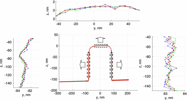
Figure 2. Measurement repeatability of the CD-AFM using a CDR-EBD tip with a nominal tip width of 70 nm.
Download figure:
Standard image High-resolution imageA critical issue in the CD-AFM is the tip wear. Despite the weak tip–sample interaction force, the geometry of the tiny AFM tip may suffer from changes due to the tip–sample interaction during the measurement. Because AFMs obtain the dilated results of the real structure by the actual tip geometry, such tip wear will directly lead to measurement instability. The long-term measurement stability by applying the CDR70-EBD tip is shown in figure 3. It can be seen that the apparent middle CD values measured on a line structure of an IVPS sample change less than 1 nm over 500 successive measurements, which takes 55 h. The result indicates the very low tip wear and very high measurement stability of the instrument.

Figure 3. Long-term stability of the CD-AFM using a CDR-EBD tip. The values shown include the effective tip width of the used CDR-EBD tip, which is approximately 70 nm.
Download figure:
Standard image High-resolution imageMeasurement of the tilting-AFM is demonstrated in figure 4, with a typical measurement profile shown in figure 5(a) and its data processing shown in figure 4(b). Since both the scanner and the AFM head are tilted with respect to the sample in our instrument configuration, the measured profile shows an incline angle of approximately 11°. To process the measured profile, the top plane of the profile is linearly fitted, shown as the red line in figure 4(a). The raw data are then matrix rotated to account for the tilting angle, which leads to the line shown in figure 4(b). It should be stressed that the levelling method, which corrects the z-coordinate of the measurement points only, should not be applied in this case, because it will distort the shape of the measured profile.

Figure 4. Measured profile of the tilting-AFM (a) and its data processing (b).
Download figure:
Standard image High-resolution image
Figure 5. (a) Measured edge profiles of 32 repeated measurements by the tilting-AFM. The inset figure shows the zoom-in details of the sidewall at the marked area and (b) evaluated sidewall angle of 32 repeat measurements.
Download figure:
Standard image High-resolution imageMoreover, it can be seen in figure 4(b) that there are many more measured data points at the right sidewall than that at the left sidewall. It is assigned intentionally in the measurement strategy, because only the profile at the right sidewall reveals the real structure, while the profile at the left sidewall indicates rather the AFM tip shape, as can be understood from the principle of the tilting-AFM shown in figure 1(b). By linearly fitting a defined part of the sidewall profile, the sidewall angle can be determined. In this example, we calculate the sidewall angle from the part of the sidewall profile with heights within  H and
H and  H, where H is the feature height.
Also the edge profiles including corner rounding and footing can be retrieved from the profile measured above. To demonstrate the repeatability of such a measurement, edge profiles obtained from 32 repeated measurements are plotted in figure 5(a) with part of their sidewall profiles detailed in the inset. Because of the small tip radius (nominal value of 2 nm) of the applied super sharp tip, the obtained edge profile should be very close to that of the real structure. The stability of the evaluated sidewall angle is shown in figure 5(b). The variation is due to both the sidewall roughness of the structure and to measurement noise of the instrument.
2.3. Traceability
Traceability is a fundamental issue for nano-dimensional metrology. The lack of traceability in measurements inhibits the comparison of tools from different manufacturers and limits knowledge about the real size of fabricated features [8]. For realizing traceable AFM CD measurements, two important issues need to be met, the calibration of the AFM's displacement scales and the effective tip geometry.
Thanks to the development of state-of-the-art metrological AFMs [9, 10], currently the scaling factors of AFMs can be calibrated with a relative uncertainty of better than 10−3. Consequently, this contribution to the overall measurement uncertainty of CD metrology is typically insignificant, especially for the small feature sizes of the current technology node.
Traceable calibration of the effective tip geometry remains a challenging task today. We calibrate the effective tip geometry by applying reference structures whose real geometry is accurately and traceably determined by applying transmission electron microscopes (TEM). A detailed study has been published recently and the readers are referred to [11]. Two methods have been applied for achieving measurement traceability, as shown in figure 6. The first method applies the silicon crystal lattice as an internal rule. As shown in figure 6(a), the structure geometry can be calculated by counting the number of crystal planes inside the structure, N, and the silicon crystal constant d111, which was determined traceably as 313.560 11(17) pm by combined x-ray and optical interferometry from bulk silicon material [12]. This method is highly accurate; however, it demands that the sample material is a single crystal. To solve this problem, an alternative method has been developed, as shown in figure 6(b). Using this method, the pitch L of line features was accurately and traceably calibrated in advance, for instance, by a metrological AFM [9, 10]. After the line features were imaged in a TEM, the pitch (M) and width (N) of the feature pair could be determined in pixel units. Thus, the scaling factor of the TEM image could be calculated as K = L/M nm pixel−1 and the width of the structure could be evaluated as W = N × L/M. An important idea underlying the proposed method is that unlike CD metrology, the pitch calibration using AFMs is independent of tip geometry.

Figure 6. Two strategies applied in traceable calibration of the geometry of the reference nano structure based on its transmission microscopic images (a) via silicon crystal lattice constant and (b) via metrological AFM.
Download figure:
Standard image High-resolution imageThe traceability chains of the two methods mentioned above are quite different. In the first method, the traceability chain is ensured via the lattice constant in the Si single crystal TEM lamella, x-ray interferometry in Si bulk material, optical interferometry and then to the optical wavelength and the metre definition of the International System of Units, the SI; while in the second method, the traceability chain is ensured via the AFM sample stage position measured by laser interferometer and then to the optical wavelength and the SI metre definition. Consistency of these two methods has been verified in our previous study [11].
3. Measurement results
The measurements were performed on an EUV test photomask. It was provided by AMTC Dresden [13] within the joint research project CDuR32 supported by BMBF. In this study, the measured AFM results are further compared to those of an EUV scatterometer developed at the radiometry beam line of the PTB at the BESSY II facility in Berlin. Since the two instruments have totally different measurement principles and traceability chains, such a comparison offers a very important and valuable cross check of both methods.
3.1. Photomask and the measurement locations
The photomask has a size of 152 mm × 152 mm. It is partitioned in 11 × 11 dies, labelled as A1–K11. Each die contains 4 × 4 fields, including the test fields with x- and y-grating patterns, and unstructured areas for reflectance measurements. The x- and y-grating patterns in different dies have different nominal CDs (90–500 nm) and different line/space ratio (1:20–20:1). A detailed description of the mask architecture can be found in [14]. The mask layer's structure is shown in figure 7.
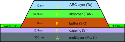
Figure 7. Layers of the photomask structure.
Download figure:
Standard image High-resolution imageSince the measurement spot size of the EUV scatterometer (about 0.7 mm × 0.7 mm) is much larger than the measurement range of the AFM, to achieve a reasonable comparison between two instruments, the grating patterns are measured by AFM at five locations marked as centre, left, right, top and bottom, as shown in figure 8. The averaged value of the results obtained at five locations is then compared with the scatterometric result.
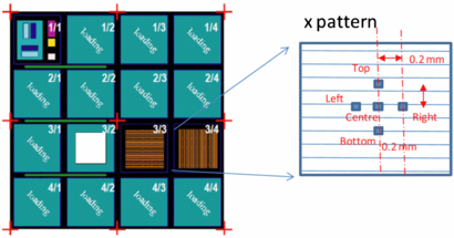
Figure 8. Five selected measurement positions on the feature pattern of a EUV photomask.
Download figure:
Standard image High-resolution image3.2. Surface roughness
The first measurement was performed to investigate the surface roughness of the grating pattern. The measurement was carried out by tilting-AFM using a super sharp AFM tip-type SSS-NCLR. The AFM images obtained at the top and the bottom planes of the y-grating pattern in the die F6 are shown in figures 9(a) and (b), respectively. Only a narrow area is measured at the bottom plane due to the small groove width of the grating pattern. The cross-sectional profiles of the images at the marked positions are also shown. Repeated measurements confirmed that the measured roughness is from the real surface rather than the instrument noise. Interestingly, it can be seen that the roughness of the bottom plane (Ra = 1.19 nm) is much larger than that of the top plane (Ra = 0.51 nm). The reason for that is not clear yet, however, we expect that it is due to the lithography process.

Figure 9. Measured surface roughness at the top (a) and bottom (b) plane of the y-grating pattern of die F6.
Download figure:
Standard image High-resolution image3.3. CD, sidewall angle and feature height
The CD of the feature patterns was measured with CD-AFM using an AFM tip-type CDR-70, which had a nominal tip width of 70 nm. Before the measurement, the tip geometries such as the effective tip width Dt and the vertical edge height (VEH) were determined as 78.0 nm and 19.8 nm, respectively, by applying a PTB reference CD structure. The measurement with the CD-AFM was performed in the vertical oscillation mode. The driving frequency was set slightly below the vertical resonance frequency of the cantilever and the structure was probed at a velocity of 1000 nm per second. A typical image of x-grating structure of the die H5 is shown in figure 10 as an example.
Figure 10. A typical CD-AFM image measured from the x-grating of the die H5.
Download figure:
Standard image High-resolution imageUnlike our reference CD structure which has a vertical sidewall, the line feature of the photomask has a sidewall angle of about 82°. This fact makes the data evaluation for the photomask measurement more complicated due to the higher order tip effect [8]. In this paper, we evaluated the measured data by taking this kind of higher order tip effect into account. Figure 11(a) illustrates the measurement of a structure with vertical sidewalls, where the blue and red curves stand for the real and measured profiles, respectively. In such a case, the outermost points of the tip extrusion probe the left and right sidewalls of the structure. The apparent middle CD of the feature can be evaluated at the height H1 = H/2 − VEH from the measured profile shown in red, where H is the height of the line feature. The real middle CD can then be calculated by subtracting the effective tip width Dt from the apparent CD, as shown in figure 11(c). However, when the photomask's line feature with non-vertical sidewalls is measured, it is the tangency point between the tip flank and the surface rather than the outermost points of the tip extrusion which probes the sidewall. Consequently, the apparent middle CD should be determined at the profile height of H1 = H/2 − VEH + Rf*cos θ, as shown in figure 11(b), where H is the height of the line feature, Rf is the vertical radius of the tip flank and θ is the sidewall angle. The real middle CD should be calculated by subtracting the effective tip width D = Dt − 2Rf (1 − sin θ) from the apparent CD, as shown in figure 11(d).
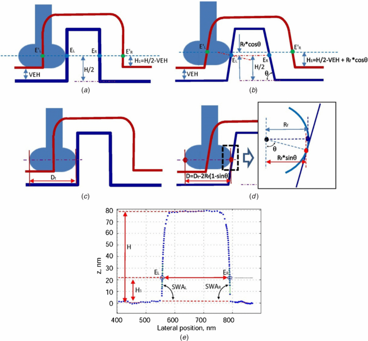
Figure 11. (a) Evaluation of the apparent middle CD for the reference structure with vertical sidewalls; (b) evaluation of the apparent middle CD for the photomask structure with non-vertical sidewalls; (c) correction of the effective tip width for the reference structure with vertical sidewall; (d) correction of the effective tip width for the photomask structure with non-vertical sidewall and (e) an example showing the evaluation of middle CD and sidewall angles from the measurement profile.
Download figure:
Standard image High-resolution imageAn example of evaluation of CD from the measured photomask profile is demonstrated in figure 11(e). The inclination of the profile was firstly removed by linearly fitting its baseline. Three segments of the profile at the left and right bottom regions and at the top region were then selected for calculating the feature height H. It should be noted that the distance from the profile segments to the corners of the structure should be properly selected (one-third of the line width was used in this study) so that the corner rounding regions are excluded, which would otherwise impact the accuracy in calculating the feature height. The height threshold value H1 needed for calculating the middle CD is then calculated (21.65 nm in this example). For achieving better statistical performance, the parts of the left and right sidewall profiles within the z range of H1 – ΔH and H1 + ΔH are linearly fitted, where ΔH defines the length of profile for fitting (10 nm in this example). In such a way, the sidewall angles SWAL and SWAR can be determined as the slopes of the fitted linear curve. The intersection points between the fitted curves and the threshold line z = H1 are calculated and are regarded as the edge positions marked as EL and ER. The distance between the points EL and ER is calculated as the apparent middle CD (236.1 nm in this example). After correcting the effective tip width D = 77.7 nm, the final middle CD of the structure is determined as 158.4 nm from the measured profile.
Two line features were measured and eight profiles were obtained at each measurement location. After applying the data evaluation mentioned above, one could obtain 16 sets of middle CD values, left and right sidewall angle values. They are then averaged to obtain the measurement results at that location. Tables 1–3 summarize the measured results of five different locations of eight different grating patterns and dies. It can be seen in table 1 that the standard deviation of the middle CD at different locations may reach 2.0 nm. This is mainly due to the width variation of the structures at different locations, since the measurement repeatability of the instrument is confirmed to be much better (1σ ≈ 0.1 nm). It can be seen in tables 2 and 3 that the sidewall angle lies within 80°–85°, indicating that the sidewall is not very steep. The standard deviation of sidewall angles measured at different locations may reach 0.8°. It is partly due to the LER and partly due to the measurement noise of the instrument. Since the profile length used for sidewall fitting is very short (about 20 nm only), even slight measurement noise will significantly disturb the evaluated sidewall angle. In addition, it can be seen that the sidewall angles at the left and right sidewalls are very similar, indicating the good symmetry of the line features. The sidewall angles can also be obtained from the tilting-AFM measurements, as already demonstrated in figure 4. Comparison of the results from two measurements indicates good agreement.
Table 1. Measured middle CD values of the selected feature patterns of the EUV photomask (see figure 9); all data are in nm.
| Measurement location | |||||||
|---|---|---|---|---|---|---|---|
| Patterns | Centre | Left | Right | Top | Bottom | Mean | Standard deviation |
| D4_3_4 | 559.26 | 561.39 | 558.59 | 556.75 | 556.39 | 558.48 | 2.03 |
| F6_3_4 | 565.58 | 564.47 | 564.56 | 566.78 | 565.39 | 565.36 | 0.93 |
| D8_3_4 | 556.10 | 552.68 | 554.94 | 556.08 | 555.84 | 555.13 | 1.45 |
| H8_3_4 | 560.17 | 559.59 | 561.94 | 559.13 | 561.49 | 560.46 | 1.21 |
| H4_3_3 | 149.51 | 153.26 | 151.25 | 152.09 | 152.34 | 151.69 | 1.41 |
| H5_3_3 | 154.09 | 154.14 | 152.39 | 153.22 | 152.89 | 153.35 | 0.76 |
| F5_3_3 | 193.30 | 191.50 | 196.01 | 194.89 | 192.24 | 193.59 | 1.86 |
| G5_3_3 | 176.10 | 175.70 | 174.45 | 173.98 | 174.03 | 174.85 | 0.98 |
Table 2. Measured left sidewall angle of the selected feature patterns of the EUV photomask; (see figure 9) all data are in degrees.
| Measurement location | |||||||
|---|---|---|---|---|---|---|---|
| Patterns | Centre | Left | Right | Top | Bottom | Mean | Standard deviation |
| D4_3_4 | 83.13 | 83.65 | 82.49 | 81.91 | 82.89 | 82.81 | 0.65 |
| F6_3_4 | 82.26 | 83.45 | 82.67 | 83.39 | 83.22 | 83.00 | 0.52 |
| D8_3_4 | 84.77 | 83.62 | 83.99 | 85.19 | 84.27 | 84.37 | 0.62 |
| H8_3_4 | 80.82 | 80.53 | 79.96 | 81.61 | 80.40 | 80.67 | 0.61 |
| H4_3_3 | 81.13 | 81.32 | 82.49 | 80.52 | 81.49 | 81.39 | 0.72 |
| H5_3_3 | 81.73 | 80.86 | 81.15 | 81.33 | 82.10 | 81.44 | 0.49 |
| F5_3_3 | 83.03 | 83.07 | 82.17 | 81.81 | 83.34 | 82.68 | 0.66 |
| G5_3_3 | 82.54 | 82.34 | 82.71 | 82.42 | 82.21 | 82.44 | 0.19 |
Table 3. Measured right sidewall angle of the selected feature patterns of the EUV photomask (see figure 9); all data are in degrees.
| Measurement location | |||||||
|---|---|---|---|---|---|---|---|
| Patterns | Centre | Left | Right | Top | Bottom | Mean | Standard deviation |
| D4_3_4 | 82.41 | 83.08 | 82.84 | 82.43 | 81.06 | 82.37 | 0.78 |
| F6_3_4 | 81.81 | 81.47 | 81.69 | 80.99 | 81.50 | 81.49 | 0.31 |
| D8_3_4 | 84.04 | 84.87 | 84.30 | 84.49 | 84.58 | 84.46 | 0.31 |
| H8_3_4 | 81.59 | 81.49 | 81.29 | 80.92 | 80.77 | 81.21 | 0.35 |
| H4_3_3 | 81.17 | 81.49 | 81.35 | 81.35 | 81.29 | 81.33 | 0.12 |
| H5_3_3 | 80.59 | 81.23 | 82.29 | 80.66 | 81.99 | 81.35 | 0.77 |
| F5_3_3 | 81.64 | 81.90 | 82.11 | 82.34 | 82.50 | 82.10 | 0.34 |
| G5_3_3 | 82.00 | 81.72 | 81.21 | 81.69 | 81.78 | 81.68 | 0.29 |
During the evaluation of CD mentioned above, the feature height H can also be obtained. Similar to the CD and sidewall angles, table 4 summarizes the feature height measured from five different locations of eight different grating patterns and dies. It can be seen that the standard deviation of height values is smaller than 0.4 nm and the feature heights of different dies are similar, indicating good uniformity of the layer thickness over the photomask. The feature height can also be obtained from the tilting-AFM measurements, as already demonstrated in figure 4. Comparison of the results from two measurements indicates good agreement.
Table 4. Measured structure height of the selected feature patterns of the EUV photomask (see figure 9); all data are in nm.
| Measurement location | |||||||
|---|---|---|---|---|---|---|---|
| Patterns | Centre | Left | Right | Top | Bottom | Mean | Standard deviation |
| D4_3_4 | 79.51 | 80.17 | 79.81 | 80.13 | 79.86 | 79.9 | 0.27 |
| F6_3_4 | 79.03 | 79.44 | 79.49 | 79.39 | 79.06 | 79.28 | 0.22 |
| D8_3_4 | 80.41 | 79.68 | 80.00 | 79.74 | 79.89 | 79.94 | 0.29 |
| H8_3_4 | 79.56 | 79.27 | 79.50 | 79.73 | 79.67 | 79.55 | 0.18 |
| H4_3_3 | 78.86 | 79.36 | 79.03 | 79.02 | 79.47 | 79.15 | 0.26 |
| H5_3_3 | 78.69 | 79.11 | 78.77 | 79.06 | 78.38 | 78.80 | 0.30 |
| F5_3_3 | 78.80 | 78.76 | 78.76 | 78.63 | 78.57 | 78.70 | 0.10 |
| G5_3_3 | 78.44 | 78.93 | 78.76 | 78.90 | 78.76 | 78.76 | 0.20 |
3.4. LER and structure position deviation
LER is one of the important parameters indicating the quality of the line feature. The measurement of LER becomes increasingly important, since with respect to the smaller CD in modern lithography tools today, LER becomes more significant.
LER and structure position deviations of structures will significantly affect the diffraction patterns measured in scatterometry [14]. As scatterometry is widely applied for in-line measurements for process control in the semiconductor industry, it is very important to accurately measure the LER and the structure positive deviation and to study their influence on scatterometric measurements.
The developed AFM is able to probe surfaces in three dimensions (x, y and z) and measures surfaces in an arbitrary plane (xz, yz and xy etc). This feature allows us very convenient and direct measurements of sidewalls along the feature line. To demonstrate such capability, typical LER profiles measured using the CDR-70 probe are depicted in figure 12(a). Each profile contains 2000 sampled pixels over a profile length of 10 µm. Three profiles measured at different height positions show a similar profile, indicating that the sidewall topography has through variations from the top plane to the bottom plane. The power spectrum density curve of the measured LER profile is calculated and shown in figure 12(b).
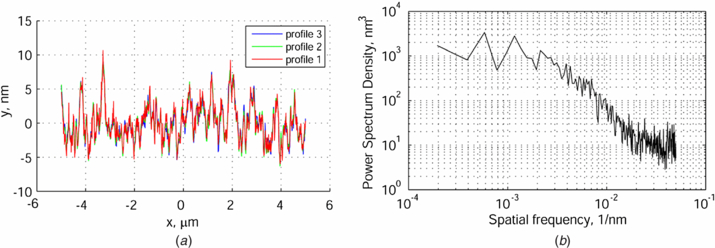
Figure 12. Measured LER profiles at the right sidewall of a line feature of the pattern F5 shown in (a) and its power spectrum density curve in (b).
Download figure:
Standard image High-resolution imageTo measure the position deviation curve of structures, ten grating lines are measured by the CD-AFM using the CDR-70 probe. Eight profiles are obtained in one measurement and one typical profile is shown in figure 13(a). Using a similar data evaluation method as for CD, the left and right edge positions of each structure can be determined and the structure position is calculated as the middle value of two edge positions. By linearly fitting the structure index and the structure position, one then obtains the mean pitch of the grating [15]. The residual error from the fitting is referred as the position deviation of the grating, which means the position deviation of the individual grating structure to an ideally uniform grating [15]. The calculated position deviation curves from eight measured profiles are depicted in figure 13(b). It can be seen that the position deviations may reach 4 nm or even more. In addition, they differ a lot even between neighbouring profiles. However, when the slow measurement axis is disabled and the same profile is repeatedly measured, the position deviation curve shows excellent repeatability as shown in figure 13(c). This result indicates that the position deviation curves shown in (b) reveal the real properties of the grating.
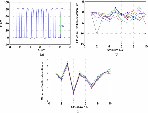
Figure 13. Measurement results for determining the structure position deviation of the feature pattern shown as (a) a profile across ten structures and the evaluation of the structure position and (b) the position deviation curves of eight measured profiles. The stability of the measurement is plotted in (c), showing the position deviation curve measured at the same location in eight repeat measurements.
Download figure:
Standard image High-resolution imageThe measured information on LER and position deviation curves has been fed to the research on the scatterometric modelling. Its comparison with the scatterometric measurements is currently under study.
4. Comparison of the AFM and EUV scatterometric results
The AFM measurement results obtained on the photomask have been further compared with that of scatterometric measurements to achieve cross verification of different techniques. For scatterometric measurements, the PTB EUV reflectometer at the electron storage ring BESSY II described in [16] is applied. The schematic diagram of the instrument is shown in figure 14(a). During the EUV scatterometric measurements, the data were obtained at a fixed angle of incidence at 6° for three different wavelengths between 13.4 nm and 13.9 nm and with s-polarized light.
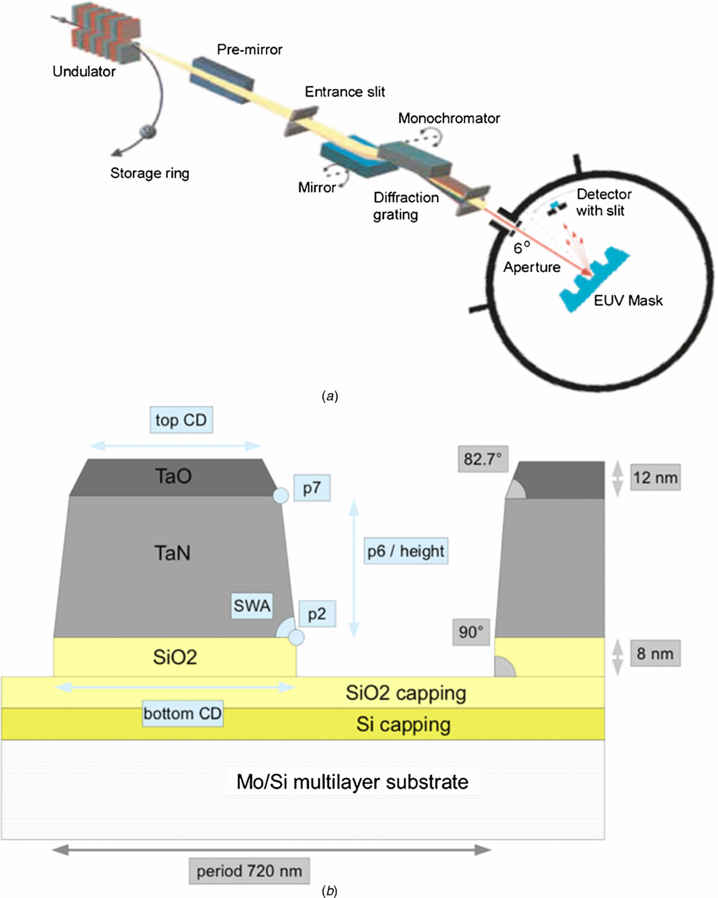
Figure 14. Schematic diagram showing the measurement setup of the PTB EUV scatterometer in (a) and the model used solving the inverse problem in (b).
Download figure:
Standard image High-resolution imageSince scatterometry is a non-imaging, indirect measurement method, proper post-processing of the measurement data is essential. The first part in this post-processing is to model the interaction of light with matter in dependence on the structure's dimensional parameters, bottom CD, top CD and height, parameterized as p2, p7 and p6 in figure 14(b). This step is usually referred to as the forward problem and is based on the solution of the Maxwell's equations which can be reduced to the 2D Helmholtz equation if geometry and material properties are invariant in one direction. The second part is the actual estimation of the structure's dimensional parameters, usually called the inverse problem. The scatterometric results used for the presented comparison were obtained by applying the finite element method to solve the forward problem and the maximum likelihood approach to solve the inverse problem. The details were described in previous papers [17–19] and for brevity, only the essentials are given here.
Besides the measurement error stemming from the measurement noise, other systematic errors need to be taken into account for obtaining a reliable estimation of the structure's parameters. These errors include the roughness effects as well as the thickness variations in the underlying substrate which is composed of two capping layers and a multilayer system. The corresponding parameters are denoted by σΔ for describing the line roughness and ν for the substrate, respectively.
Supposing independent measurements and considering the impact of the line roughness by an exponential damping factor (cf [18]), the measurement errors of the jth data point can be modelled as being normally distributed with zero mean. Their variances are composed of two independent random variables, such that
The first term  indicates the contribution of the damped efficiencies. The second term b2 is the contribution of the background noise independent of the measured light intensities. The calculated efficiencies for the different diffraction orders are denoted as
  . They are the solutions of the forward problem in dependence on the geometrical profile parameters
  of the absorber lines and the substrate parameters
  . The parameter nj indicates the diffraction order of the jth measured value and d is the period of the line-space structure of the mask field.
Denoting the measured efficiencies by  , the following likelihood function was used:
The maximization of the likelihood function  yields estimates of the wanted parameters and their uncertainties can be expressed in terms of the negative second derivative of the logarithm of
  , the so-called Fisher-information matrix (cf [19]).
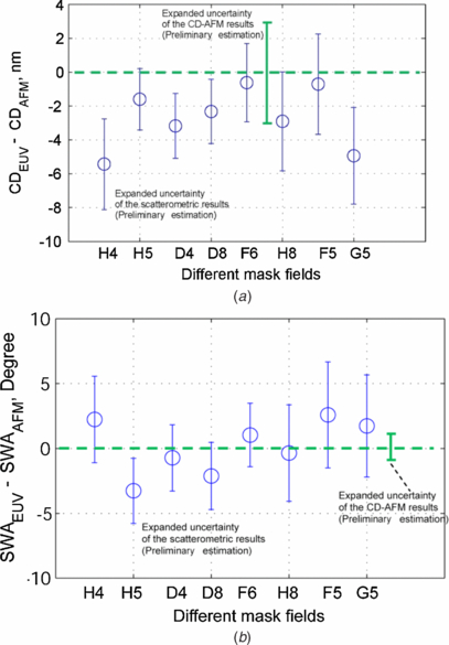
The comparison on the middle CD values measured by the AFM and the EUV scatterometer is shown in figure 15(a). For clarity, the y axis of the figure shows the difference between EUV scatterometric results (CDEUV) and the AFM results (CDAFM) only. From the measured CD values of the AFM given in the table 1, the middle CD values of the EUV scatterometer can be easily derived. It should be noted that for the applied EUV scatterometry, only the top and bottom CD are determined after solving the inverse problem using the maximum likelihood approach. For comparison purposes, we calculated the middle CD from the top and bottom CD based on the model shown in figure 14(b).
Figure 15. Comparison of the measurement results obtained by the CD-AFM and EUV scatterometer shown as (a) the measured middle CD and (b) the measured sidewall angles. For clarity, the difference of the AFM and scatterometer results is plotted. The error bars given show the preliminarily estimated expanded uncertainty (k = 2) of both methods.
Download figure:
Standard image High-resolution image
Figure 15(a) shows good agreement between the two methods with respect to the preliminary estimated expanded uncertainty. The spread of most points is within ±2 nm. However, there is still a remaining offset of 2.7 nm between both methods. The reason for this offset should be investigated in the future. The possible reasons for this deviation could be, for instance, the high-order tip effects, the systematic error in the applied reference CD structure, the limited modelling of the scatterometric measurement or the CD non-uniformity of the grating pattern between the relative large area measured by the scatterometer and the local small areas measured by the AFM. Nevertheless, the agreement is very promising since the values being compared are absolute CD values, which are measured by two instruments with totally different principles and traceability chains.
The comparison between the sidewall angles of the AFM and the scatterometric results is shown in figure 15(b). Similarly, the y axis of the figure indicates the difference between EUV scatterometric results (SWAEUV) and the AFM results (SWAAFM) for clarity. Again, we can see quite good agreement between the two sets of results with respect to their preliminary estimated measurement uncertainty. The spread of most points is within about ±2°.
5. Conclusion
Critical dimension and sidewall profile of EUV photomask structures were measured by using two kinds of AFM techniques, CD-AFM and tilting-AFM. The CD-AFM applies flared tip, which is capable of measuring CD, feature height, left and right sidewall angle, LER and structure position deviation. However, the large and complex geometry of the flared tip limits its spatial resolution and the measurement capability of corner rounding and footing. In contrast, the tilting-AFM may apply super sharp tips, offering high spatial resolution. However, the tilting-AFM needs rotation of the structure/tip to make the other sidewall measurable, leading to difficulties in measuring the CD. Both techniques are applied complementarily in this study, adding their strengths and overcoming their limitations.
Traceability is a fundamental issue for AFM nano metrology. As the calibration of the scaling factors of scanners can be well satisfied by metrological AFMs today, the calibration of the effective tip geometry remains a challenging issue. In this study, a PTB reference structure, whose real geometry was accurately and traceably calibrated by TEMs using either the silicon crystal lattice or the pitch of structures as an internal scale, is applied for this purpose.
CD, left and right sidewall angle, feature height, LER and structure edge profiles of eight grating patterns in different dies of a test EUV photomask have been measured using the developed instrument. A data evaluation method with considered higher order tip effect due to the non-vertical sidewall has been introduced. Measurement results have been summarized in tables 1–4. The grating patterns are measured at five locations. The standard deviation of the middle CD at different locations may reach 2.0 nm. It is mainly due to the width variation of the structures at different locations, since the measurement repeatability of the instrument is confirmed to be much better (1σ ≈ 0.1 nm). The sidewall angle of structures lies about 80°–85°, indicating that the sidewall is not very steep. The standard deviation of sidewall angles measured at different locations may reach 0.8°. It is partly due to the line edge roughness and partly due to the measurement noise of the instrument. In addition, the sidewall angles at the left and right sidewalls of structures are very similar, indicating the good symmetry of the line features. The standard deviation of height values is smaller than 0.4 nm and the feature heights of different dies are similar, indicating good uniformity of the layer thickness over the photomask. Finally, the AFM results are compared to that of a PTB EUV scatterometer regarding the values for the middle CD and the sidewall angle. The result yields a linear relation within a spread of only about ±2 nm and an offset of the absolute values below 3 nm. For the side wall angle, both methods yield consistent results within a range of about ±2°.
Further studies will be carried out to investigate the remaining offsets between the AFM and scatterometric measurements and to estimate their measurement uncertainty budgets. Furthermore, the LER results of both methods will be compared.
Acknowledgment
The EMRP is jointly funded by the EMRP participating countries within EURAMET and the European Union. We thank the European commission and the EURAMET e. v. for financial support under the support code no 912/2009/EC.