

Abstract
The thickness and temperature dependence of in situ grown cobalt thin films on Cr2O3(0 0 0 1) single crystalline substrate has been studied by low energy electron microscopy (LEEM). The LEEM images indicate that growth of thin Co films (⩽5 monolayers) on chromia at 100 K tends to be continuous and flat with suppressed island growth compared to films grown on chromia at room temperature and above (to ~440 K). Low energy electron diffraction indicates that disorder builds and crystallinity of the cobalt thin film decreases with increased film thickness. Compared with cobalt thin films on Al2O3(0 0 0 1) single crystalline substrate, cobalt thin films on Cr2O3(0 0 0 1) show larger magnetic contrast in magnetic force microscopy indicating enhancement of perpendicular anisotropy induced by Cr2O3.
Export citation and abstract BibTeX RIS
Introduction
Perpendicular exchange-bias structures, based on the antiferromagnetic and magneto-electric Cr2O3(0 0 0 1), have drawn considerable attention, in part because of potential applications in voltage controlled spintronics [1–6]. The boundary spin polarization [1, 7–10], at the surface of the magneto-electric Cr2O3(0 0 0 1), can be isothermally voltage-controlled to provide perpendicular voltage-controlled exchange-bias in an adjacent ferromagnet [1]. This means that the adjacent ferromagnet is typically chosen with perpendicular magnetic anisotropy, e.g. Co-Pd or Co Pt multilayers.
The metal adlayers do not necessarily obscure the boundary spin polarization [9, 11] known to occur at the free surface of the magneto-electric Cr2O3(0 0 0 1). The compelling evidence of voltage controlled exchange bias [1, 2, 9, 12–16] supports the contention that the chromia interface polarization can be preserved at a buried interface, since it is the interface polarization of the magneto-electric Cr2O3(0 0 0 1) that is key. This applied even to the Co/Cr2O3(0 0 0 1) interface [15, 16]. The interaction of a ferromagnetic film, with a tendency for in-plane magnetization, with a surface with perpendicular spin polarization (like chromia), can be complex. While Co thin films tend to have an in-plane anisotropy, the magnetic coupling at the interface of Co/Cr2O3(0 0 0 1) gives rise to a rich array of magnetic phenomena [11, 15–24]. There is a strong temperature dependence of the exchange bias [11, 17] and magnetic anisotropy [18–20] in the Co/Cr2O3(00 0 1) system. Signatures of the complexities with the Co/Cr2O3(0 0 0 1) system are the observed strongly enhanced tendency for perpendicular anisotropy with a Pt [15, 20–22] or Au [23] capping layer on the Co/Cr2O3(0 0 0 1) heterostructure. There is evidence of uncompensated Cr antiferromagnetic spins localized in the vicinity of the Co/Cr2O3(0 0 0 1) interface [11].
The cobalt film morphology [22, 23] will profoundly affect its magnetic anisotropy, and thus is an important consideration when seeking understanding of the complex temperature dependence of the exchange bias in a Co/Cr2O3(0 0 0 1) heterostructure. On metal substrates, the growth of cobalt is strongly related to the growth temperature [25–28]. While cobalt thin film growth tends to form islands, following a Volmer-Weber growth mode on oxide substrates at room temperature [22, 29], cobalt growth on magnetically ordered oxide substrates, such as Cr2O3(0 0 0 1), has been very sparsely investigated for substrate temperatures below room temperature and thus below the antiferromagnetic ordering temperature. To add some clarity to the issues surrounding cobalt growth on an antiferromagnetic oxide substrate with high boundary polarization, we have investigated the temperature dependent growth and the magnetism of Co on Cr2O3(0 0 0 1).
Methods and experiment details
Before deposition of the cobalt film, the Cr2O3(00 0 1) single crystal substrate surfaces were prepared under ultrahigh vacuum conditions by Ar+ ion sputtering at 1 kV for half an hour and then annealed, as outlined in previous work [1, 10, 30, 31]. The surface order was established by low energy electron diffraction (LEED). The cobalt adlayer was deposited through e-beam thermal deposition at rate of ~2 min per monolayer on Cr2O3(0 0 0 1) at various chromia substrate temperatures. The cobalt growth rate was calibrated against growth of cobalt on copper substrates.
The low-energy electron microscopy (LEEM) characterization is one of the in situ techniques that are able to monitor the growth during the growth process. As described elsewhere [32], LEEM was used to observe the growth and morphology of the cobalt overlayer at the surface of Cr2O3(0 0 0 1). The base pressure of the LEEM chamber was in 10−11 torr range, suppressing oxidization of the Co adlayer during growth and the LEEM measurements. All the LEEM measurements (LEEM Image or LEEM I/V spectra) were done at the corresponding growth temperature.
The MFM images acquired by a Bruker-ICON magnetic force microscopy using high-performance MFM Probes (MESP-RC-V2, Bruker) with a magnetic Cobalt-Chromium coating. The Co/Cr hard magnetic coated MFM tips are tailored for high-sensitivity and magnetic contrast. The magnetization of the MFM tip is perpendicular to the sample surface and points downward, in the geometry of our experiment. All the MFM images were obtained using the phase modulation detection mode due to its ease of use, better signal-to-noise ratio, and reduced artifacts content. The magnetic tip was kept at a lift height of 20 nm over the sample surface and was oscillated at resonance frequency (tapping/lift mode). As the MFM tip was scanned across the sample surface, the strength of the magnetic interaction between the tip and the magnetic stray fields of the sample results in a phase shift in the oscillation, the basis for the MFM mapping shown here. The MFM phase images here are a measure of the phase lag between the drive voltage and the cantilever response, and illustrative of the magnetic force gradient distribution on a sample's surface. The ~16 monolayer thick cobalt adlayer film on chromia, with a native CoO surface, was selected for further magneto-optic Kerr effect (MOKE) and magnetic force microscopy (MFM) measurements.
As a check the magnetic anisotropy and cobalt film morphology, CoO/Co/Cr2O3(0 0 0 1) and CoO/Co/Al2O3(0 0 0 1) heterostructures were compared both above and below the Néel temperature (307 K) of chromia. The cobalt films on Al2O3(0 0 0 1) were deposited by thermal evaporation under ultrahigh vacuum conditions at 0.1 Å min−1. To investigate the magnetic anisotropy of Co/Cr2O3(0 0 0 1), we performed the measurement of the magneto-optic kerr effect (MOKE). An intensity stabilized helium-neon laser beam of wavelength 632.8 nm with an output power of >1.0 mW was used for MOKE. In the MOKE measurements, the light was then further polarized and the reflected beam periodically modulated by a photoelastic modulator with a frequency of 50 kHz, which was as a modulation reference signal for lock-in amplifier to provide phase sensitive detection for the signal from a photo-diode measuring the reflected beam off the sample.
To ascertain the film purity and composition, angle-resolved x-ray photoemission spectra were obtained using SPECS PHOIBOS 150 energy analyzer. The angle-resolved x-ray photoemission spectra (ARXPS) was used to establish that the CoO layer for the CoO/Co/Cr2O3 heterostructure was limited to a surface oxide and that the subsurface cobalt was largely free of oxidation, thus making the observed CoO largely a passivation layer. A non-monochromatized Al Kα x-ray source, with photon energy 1486.6 eV, was used with various emission angles. The core level binding energies were calibrated on the basis of a gold (Au) 4f7/2 reference peak at the binding energy of 84 eV. The LEED, MFM, MOKE and ARXPS measurements were done at room temperature.
The dependence of the cobalt adlayer morphology on growth temperature
In general, with cobalt film growth on chromia, the cobalt adlayers were seen to form a more uniform film on chromia with a growth temperature below room temperature than with cobalt film growth at room temperature, the latter being the more typical substrate temperature. For the cobalt films grown on chromia with substrate temperatures of 100 K, the LEEM intensity versus energy spectra (LEEM-I/V) indicate dynamical and kinematic scattering characteristics of an ordered film with improved flatness compared to the cobalt films grown on chromia at room temperature. In figure 1(a), kinematic scattering characteristics of an ordered film (the peak at around 14 eV in the LEEM-I/V curve) are seen in (1) but not in (2) or (3). The latter show a simple decaying LEEM-I/V intensity with increased electron energy and little evidence of dynamic and kinematic (Bragg) scattering in the very low energy intensity versus voltage curves. The LEEM images also show the films to be flatter or smoother for the cobalt films grown on chromia with substrate temperatures of 100 K (figure 1(b)) as compared to the cobalt films grown on chromia at room temperature (figure 1(c)). The LEEM did not show significant differences in crystallographic order or morphology for cobalt films grown at the low temperature 100 K and those grown at the low temperature and then annealing to room temperature.
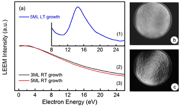
Figure 1. (a) The low-energy electron microscopy intensity versus incident electron energy (LEEM-I/V) curves. The spectra (1) is for 5 monolayer (ML) Co grown on Cr2O3(0 0 0 1) at about 100 K i.e. low temperature. The spectra (2) is for 3 ML and (3) is for 5 ML Co films grown on Cr2O3(0 0 0 1) at room temperature (RT), respectively. The LEEM images, taken at an electron energy of ~15 eV, of a 5 monolayer Co grown on Cr2O3(0 0 0 1), are shown for films grown at (b) at low temperature (100 K) and (c) at room temperature.
Download figure:
Standard image High-resolution imageThe cobalt films grown on chromia at room temperature are still not uniformly metallic as a 5 monolayer Co film grown at room temperature exhibits strong charging effects. This means that the cobalt films grown at room temperature and above show a degree of roughness which prevents the cobalt islands in the surface film from exhibiting complete percolation. The charging effect, resulting in deformed LEEM images (figure 1(c)), indicates that the dielectric properties of the chromia single crystal substrate [33] dominate and neither a conducting surface nor a metallic thin cobalt film, with percolation, exists uniformly across the surface. The cobalt films, grown on chromia at room temperature, probably follow Volmer-Weber or island growth mode, as reported for other cobalt films [22].
For cobalt films grown on chromia at substrate temperatures of 100 K, the charging effects in LEEM imaging are minimal (figure 1(b)). The low energy electron diffraction (LEED) pattern/images were taken after the gentle annealing of film to room temperature and are characteristic of cobalt adlayers with a high degree of crystallographic order, as seen in figure 2(a). The six-fold diffraction pattern from the cobalt adlayer (figure 2(a)) has the same angular orientation as the chromia substrate (figure 2(b)), even if not lattice matched. This means that likely there are multiple C3v symmetry domains of cobalt (1 1 1), where each domain maintains crystallographic registry with the C3v symmetric chromia surface, so in combination, the LEED has 6-fold symmetry. This is consistent with prior reflection high energy electron diffraction (RHEED) studies [17, 21] and x-ray diffraction [24] of cobalt on chromia.

Figure 2. (a) The low energy electron diffraction (LEED) of thin Co adlayers grown on Cr2O3(0 0 0 1) at ~100 K, and for comparison, (b) a LEED image of a clean Cr2O3(0 0 0 1) single crystal, prior to cobalt deposition. The diffraction spot-splitting is highlighted in the inset of (a) and clearly shows the Co adlayer crystallography follows the Cr2O3(0 0 0 1) substrate crystal orientation, but is not lattice matched, as there exist two closely spaced diffraction beams. The incident electron energy is 159 eV.
Download figure:
Standard image High-resolution imageFigure 3 illustrates the thickness dependence of the LEEM-I/V spectra for Co adlayers growth at 100 K ranging from ~5 monolayers to ~16 monolayers. The LEEM-I/V intensity decreases and shifts in energy with the increasing of Co thin film thickness. This indicates that not only are the thinner films more crystalline, but the thinner films tend to grow uniform layers as indicated by the plateaus and sharp drops in the 15 eV LEEM-I/V peak at nominally 6 and 8 monolayers of cobalt (figure 3). The diminished LEED diffraction beam intensities measured for thicker cobalt adlayers (some 14 to 16 monolayers) on chromia indicate that such films contain more disorder than the thinner (5 to 6 monolayers), more crystalline, cobalt films grown on chromia with substrate temperatures of 100 K. This is consistent with the greater roughness (6.37 nm to 8.24 nm root mean square roughness) seen in atomic force microscopy (AFM) (figures 4(a) and (c)), as well as with the LEEM results of figure 3. By way of comparison, Co grown on Al2O3(0 0 0 1) single crystals, at room temperature, results in cobalt adlayer films that are very flat and uniform (root mean square roughness of about 0.16 nm), preserving the terrace and step structure of the Al2O3(0 0 0 1) single crystal surface, as seen in figure 4(e). This indicates a tendency towards layer-by-layer growths or the Frank–van der Merwe (FM) growth mode [29] for Co grown on Al2O3(0 0 0 1) single crystals. So roughness of cobalt adlayers, when grown at room temperature, is dependent upon the dielectric oxide surface chosen.
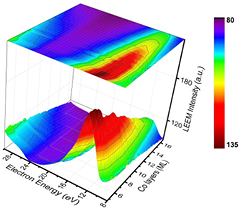
Figure 3. The cobalt thickness dependence of LEEM-I/V spectra up to a cobalt adlayer thickness of roughly ~16 monolayers. The LEEM-I/V intensities shows a scattering peak around 12–16 eV, characteristic of a crystalline cobalt adlayer, that varies with the thickness of the Co adlayers.
Download figure:
Standard image High-resolution image
Figure 4. The AFM (a, c and e) and MFM (b, d, and f) images of 16 monolayer (a, b) and 25 monolayer (c, d) cobalt adlayer thin films grown on a Cr2O3(0 0 0 1) single crystal at 100 K compared with a 16 monolayer cobalt film grown on an Al2O3(0 0 0 1) single crystal at room temperature (e, f).
Download figure:
Standard image High-resolution imageIn-plane magnetic anisotropy of the cobalt adlayer
Consistent with most studies of cobalt thin films [34–37], the easy magnetization axis resides in-plane, as is evident in magneto-optic Kerr effect MOKE studies of figure 5. The longitudinal MOKE results, illustrated in figure 5, clearly indicates that the easy axis of the 16 monolayer cobalt film, grown on Cr2O3(0 0 0 1) at ~100 K, is preferentially in-plane. The magnetic hysteresis loops indicate that the remanent magnetization of our cobalt adlayer films is small, which may reduce the sensitivity of spin-polarized low-energy electron microscopy (SPLEEM) [24] to the cobalt surface polarization. Indeed, we found that SPLEEM was insensitive to cobalt grown on chromia, providing no indication of a significant spin asymmetry intensity.
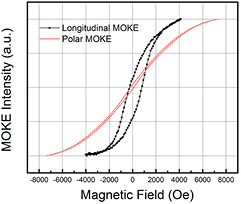
Figure 5. The MOKE derived magnetic (relative M(H)) hysteresis loop of a 16 monolayer Co adlayers grown on Cr2O3(0 0 0 1) at ~100 K, accompanied by a CoO oxidation capping layer.
Download figure:
Standard image High-resolution imageA cobalt adlayer domain structure was observed in the MFM images (figures 4(b) and (d)), and evident in the sharp bright-dark contrast. This Co/Cr2O3(0 0 0 1) MFM contrast is indicative of a large out-of-plane component of magnetization associated with each magnetic domain. MFM tip is most sensitive to variations of magnetic structure near sample surface: the magnetic moment of the tip interact with the stray fields from the sample and is sensitive to the repulsive and attractive force gradients normal to the surface. This out-of-plane magnetic contrast for Co/Cr2O3(0 0 0 1) is especially evident when comparing the images with figure 4(f), which shows the MFM of Co grown on a Al2O3(0 0 0 1) single crystal. The MFM scale for the Co/Al2O3(0 0 0 1) image is increased 10 times in (f)—on the same scale as (b) and (d), the MFM images for Co/Cr2O3(0 0 0 1), the image (f) would show no contrast. We again note that these magnetic attractive/repulsive forces cause shifts of both the resonance frequency and the phase. Many magnetic grains participate in the formation of an interaction domain in which the grains exhibit the similar orientation of magnetization (up and/or down domains), yet the MFM phase image contrast represents magnetic-force-gradient mapping largely normal to the surface. In this case, the bright domain indicates the tip is repulsive to the spot, while the black domain indicates it is attractive [38]. So the out-of plane component of magnetization is far more significant for cobalt on chromia, than cobalt on sapphire (Al2O3). The corresponding AFM images (a) and (c) show increasing grain size within the Co adlayer with increasing Co thin film thickness following growth on Cr2O3(0 0 0 1) single crystal at 100 K. The AFM image of cobalt thin film on Al2O3 shows atomic terraces (e), induced by the substrate, while the AFM images for Co/Cr2O3(0 0 0 1) do not, due to the cobalt adlayer roughness.
Figure 6 shows the differences in the x-ray photoemission (XPS) spectra before and after Ar+ ion sputtering. After Ar+ sputtering, the oxide XPS peaks characteristic of the oxidized cobalt (denoted by the arrows) are absent, indicating that the presence of oxygen evident in these XPS spectra is associated with a CoO capping layer. After removing the CoO capping layer, the cobalt adlayer is seen to be very close to pure Co metal in these XPS spectra. So the signature of CoO that appears in the XPS is dominantly the result of surface oxidation. Yet a possible role of interfacial oxidation cannot be excluded a priori. Interfacial oxidation of cobalt adlayer films has been implicated as a possible origin of perpendicular magnetization [35–37], as have other interfacial effects [17–21]. In addition, the perpendicular magnetization, resulting from the boundary magnetization of Cr2O3, provides a mechanism for strong contrast in MFM [1, 8–10]. Due to the interfacial collinear coupling between Co and Cr of Cr2O3, the cobalt adlayer film may show a large perpendicular magnetic moment [17–19] despite the tendency for cobalt to exhibit in-plane magnetic anisotropy.

Figure 6. The cobalt 2p core level XPS spectra for 16 monolayer Co adlayers grown on Cr2O3(0 0 0 1) at ~100 K before and after Ar+ sputtering. The Ar+ sputtering was done to diminish or remove a surface (but not interface) CoO oxidation capping layer. The oxidization peaks characteristic of the oxidized cobalt (shown by the arrows) are absent, indicating that the existence of oxidized cobalt is restricted to a capping layer.
Download figure:
Standard image High-resolution image
Conclusion
In the exchange bias system of Co on Cr2O3(0 0 0 1) single crystals, quality of the cobalt film is a key factor [11, 15–24]. In this work, we show that better cobalt adlayer films are grown at lower temperatures on chromia, well below room temperature. On other oxide surfaces, like Al2O3(0 0 0 1), very flat cobalt films can be grown at room temperature. The film quality does depend on film thickness, as roughness and loss of crystallinity builds in the cobalt adlayer as film thickness increases. This growth of cobalt on chromia is an example where growth at higher temperatures, to anneal out defects, does not work in favor of improved film quality.
Acknowledgments
This project was supported by the National Science Foundation through the Nebraska MRSEC (Grant No. DMR-1420645) and by the Semiconductor Research Corporation through the Center for Nanoferroic Devices, an SRC-NRI Center under Task ID 2398.001, and by C-SPIN, part of STARnet, a Semiconductor Research Corporation program sponsored by MARCO and DARPA (SRC 2381.002 and 2381.003). The LEEM experiments were performed at the Molecular Foundry, supported by the Office of Basic Energy Sciences of the U.S. Department of Energy under Contract No. DE-AC02-05CH11231. Research was performed, in part, in the Nebraska Nanoscale Facility, Nebraska Center for Materials and Nanoscience, which is supported by the National Science Foundation under Award NNCI: 1542182, and the Nebraska Research Initiative.. The authors would like to thank Prof. Xiaoshan Xu at University of Nebraska-Lincoln for providing the high quality Al2O3 single crystal substrates.