

Abstract
The orbital symmetry of the band structure of 2H-WSe2(0 0 0 1) has been investigated by means of angle-resolved photoelectron spectroscopy (ARPES) and density functional theory (DFT). The WSe2(0 0 0 1) experimental band structure is found, by ARPES, to be significantly different for states of even and odd reflection parities along both the  –
– and
and  –
– lines, in good agreement with results obtained from DFT. The light polarization dependence of the photoemission intensities from the top of the valence band for bulk WSe2(0 0 0 1) is explained by the dominance of W 5
 states around the
  -point and W 5dxy states around the
  -point, thus dominated, respectively, by states of even and odd symmetry, with respect to the
  –
– line. The splitting of the topmost valence band at
  , due to spin–orbit coupling, is measured to be 0.49 ± 0.01 eV, in agreement with the 0.48 eV value from DFT, and prior measurements for the bulk single crystal WSe2(0 0 0 1), albeit slightly smaller than the 0.513 ± 0.01 eV observed for monolayer WSe2.
Export citation and abstract BibTeX RIS
Introduction
The band structure of WSe2(0 0 0 1) [1–8] and monolayer WSe2 [1, 2, 8–26] has been studied considerably, although not as heavily investigated as other related metal dichalcogenides such as MoS2(0 0 0 1) [1, 7, 9–12, 15, 19, 20, 23, 26–44], and yet the investigation of band symmetry has not been an emphasis in prior experimental work. In spite of the low C3v symmetry of the transition metal dichacogenide surface, there is evidence of state symmetry even along directions of the Brillouin zone with no mirror plane symmetry. Recently, it was shown [27, 32] that the experimental band structure of MoS2(0 0 0 1) retains a very strong symmetry dependence along the  –
– as well as along the
  –
– lines of the surface Brillouin zone. The former is somewhat surprising because the
  –
– line of the WSe2(0 0 0 1) surface Brillouin zone does not, in principle, preserve mirror plane symmetry. Note that the
  –
– line, of the WSe2(0 0 0 1) surface Brillouin zone, is expected to preserve a mirror plane symmetry in the C3v surface symmetry.
The wave vector corresponding to the top of the valence band varies with WSe2 film thickness: at the Brillion zone edge  for monolayer WSe2 [24] and at the zone center
  for bulk WSe2(0 0 0 1). Band widths at the top of the valence band, at the zone center
  , are also expected to increase [45], as interlayer interactions lead to the formation of a bulk band structure with increasing numbers of layers. The bands, and also the frontier orbitals, at the Brillouin zone edge at
  and at the zone center
  do not share the same symmetry. The fact that the band symmetry is very much dependent upon wave vector could be of considerable importance say in catalysis and optoelectronics. The band structure of the transition metal dichalcogenide changes, as a function of layer thickness (i.e. the effect of an increasing number of layers), and has been investigated for MoS2 [1, 31, 42], WS2 [1, 45, 46] and WSe2 [1, 2]. Yet the band symmetries and spin–orbit coupling at the Brillouin zone edge
  point are little affected by an increase in numbers of layers. An accurate determination of the state symmetries of the surface bands may help in device design as well, where WSe2 is the narrow channel conductor. The much larger atomic number, Z, of the components of WSe2, as compared to that of MoS2, results in a much larger spin–orbit coupling, as evident in the band structure of WSe2(0 0 0 1) [7, 9, 10, 12, 13, 15, 20, 24]. For the same reason, the WSe2 valence band features are much better resolved and band symmetry assignments can be made with greater facility than for MoS2(0 0 0 1).
Experiment
The occupied state electronic structure of bulk WSe2 was experimentally mapped along both the  –
– and
and  –
– directions through angle-resolved photoemission spectroscopy (ARPES). The ARPES was performed at the linear undulator beamline (BL-1) [47] of the Hiroshima Synchrotron Radiation Center (HiSOR) at Hiroshima University, in Japan, at photon energies of 34 and 75 eV, as indicated. The ARPES derived experimental band structure was acquired in both p-polarization (the incident light vector potential A parallel to the mirror plane) and s-polarization (the incident light vector potential A perpendicular to the mirror plane) geometries. The use of these two different photoemission geometries provides an experimental distinction between initial valence band states with even and odd symmetries with respect to the nominal
  –
– and
and  –
– direction of the surface Brillouin zone [27, 32, 48–52]. The ARPES experiments were carried out using the angular (display) mode of the hemispherical electron analyzer (R4000, VG-Scienta), as described previously [27, 48], with a combined effective energy resolution of about 30 meV and with a wave vector resolution of 0.035 ± 0.005 Å−1 for hν = 34 eV at the Fermi level (EF). Throughout this paper, the binding energies are referenced to the Fermi energy (EF), in terms of E − EF, established from polycrystalline gold in contact with the substrate and sample holder. This placement of the Fermi level corresponded to estimates of the Fermi level obtained from the cutoff of the density of states due to defects. The ARPES was performed at room temperature.
The clean WSe2(0 0 0 1) surface was prepared by cleaving in UHV at a base pressure of better than 1 × 10⁻¹⁰ Torr. Independent inverse photoemission and x-ray photoemission studies confirm that this in situ cleaving provides a surface free of contamination. Low-energy electron diffraction (LEED) was used to verify the extent of the WSe2(0 0 0 1) surface order (figure 1(b)), as well as establish the in-plane orientation of the crystal. Figures 1(c) and (d) illustrate symmetry lines of the surface Brillouin zone at two different iso-energy surfaces (plots in kx and ky, at constant photoelectron kinetic energy) obtained by azimuthal rotation of the sample. These plots at the iso-energy surfaces of E − EF = −0.5 eV, or corresponding to the valence band maximum at the  points, and at E − EF = −1.7 eV, well below the top of the valence band, confirm the Brillouin zone and placement of the critical points established by LEED. These measurements serve as the basis for the placement of the nominal
  ,
,  and
and  high symmetry points of the surface Brillouin zone. We have confirmed that the experimental results are reproducible.
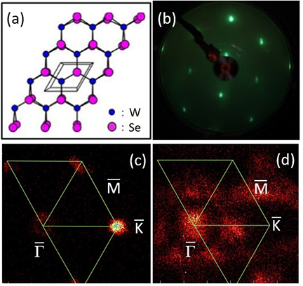
Figure 1. A schematic diagram of a WSe2 layer (a). The LEED image of the WSe2(0 0 0 1) surface taken at an incident electron energy of 85.1 eV (b). The critical points ( ) of the 2D SBZ can be detected by the iso-kinetic energy wave vector dependent and constant energy contour photoemission intensity plots. These wave vector dependent photoemission intensity plots were taken near the top of the valence band (
 = −0.5 eV) (c) and in the middle of the valence band (
 = −1.7 eV) (d). The constant energy contour plots were taken using an incident photon energy of 75 eV. The green lines indicate high symmetry lines of SBZ (
 to
to  or
or  ).
).
Download figure:
Standard image High-resolution imageTheoretical methodology
We calculated the electronic band structure along the  –
– –
– –
– lines of the WSe2(0 0 0 1) surface Brillouin zone using density functional theory (DFT) with spin–orbit coupling included. The approach used was similar to that used for single layer WSe2 [24] and MoS2(0 0 0 1) [27], where good agreement between theory and angle-resolved photoemission was obtained. We used the super cell method with a plane-wave basis set (at a cutoff energy of 500 eV) and the projector-augmented wave (PAW) [53, 54] technique for our DFT calculations, as implemented in the Vienna ab initio simulation package (VASP) [55, 56]. For describing the exchange-correlation of the electrons, we applied the generalized-gradient-approximation (GGA) Perdew–Burke–Ernzerhof (PBE) functional [57]. The total energy and force acting on each atom were then corrected by the pairwise DFT-D3 correction [58] to account for van der Waals (vdW) interactions. We sampled the Brillouin zone for the bulk and surface of WSe2(0 0 0 1) with (18 × 18 × 6) and (15 × 15 × 1) k-point meshes, respectively. The experimental lattice parameter and the interlayer distance (3.282 Å and 6.480 Å, respectively) for WSe2(0 0 0 1) [6] is in very good agreement with the optimized lattice parameter and the interlayer distance found in DFT after optimization (3.286 Å and 6.498 Å, respectively). We modelled the 2 H-WSe2(0 0 0 1) surface by a 10-layer slab of the WSe2 trilayer, meaning a slab of 10 WSe2 trilayers (i.e. 10 W and 20 Se layers in total).
The contribution of every atomic orbital (i.e. their l and m numbers) of each atom to the WSe2(0 0 0 1) valence band structure, as plotted in figure 2, was assessed to resolve the symmetry character of the corresponding wave-functions. Subsequently, to produce the even and odd symmetry band structure, we sum all projected components contributed from the atoms in the top three WSe2 layers that correspond to even (s, px, pz, dxz,  ,
,  ) or odd (py, dxy, dyz) symmetries, respectively, with respect to the mirror plane (xz). No corrections were made for finite temperature nor any final state effects in our model calculations. The placement of the Fermi level was adjusted for the DFT calculations to align the top of the calculated valance band with that obtained in the experimental band structure from the ARPES measurements, i.e. increasing the binding energy by 0.9 eV as an offset to the calculated band structure. Even though there is general agreement with experimental data, the binding energies of occupied bands obtained in theory are slightly off, as the band width is more narrow in theory than experiment. We thus increased the calculated band structure width by 6% to better align with experiment. Our DFT simulations indicate that the distances between WSe2 layers are virtually unchanged between the surface and the bulk. Consistent with our expectations, because the weak interlayer (vdW like) interactions, the distance between the two top most surfaces has changed only slightly, if at all, from the bulk. The tiny potential surface lattice relaxation results in only very small perturbations to the band structure that are beyond the accuracy of our ARPES measurements.
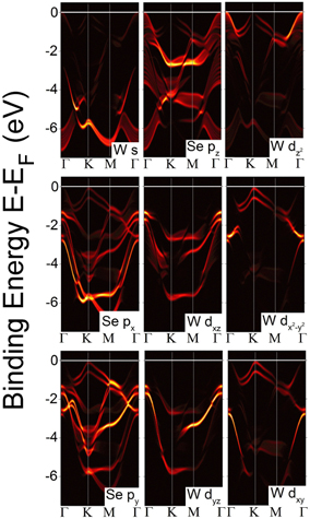
Figure 2. A comparison of the various orbital component contributions to the WSe2(0 0 0 1) valance band structure obtained from DFT. The results for these various component plots are not offset or rescaled, so the binding energy is determined from the top of the calculated band structure.
Download figure:
Standard image High-resolution imageSymmetry selection along the SBZ line ( – and –)


Using linearly polarized light from the synchrotron light source, we exploited the dipole symmetry selection rules for photoemission [27, 32, 48–52] to clarify the symmetry properties of the various bands of WSe2(0 0 0 1). The symmetry of 'bulk' 2H-WSe2 belongs to the nonsymmorphic [59] space group  [39] with a strong covalent intralayer bonding, but weak bonding between adjacent layers [3, 6]. The point group symmetry of 2H-WSe2(0 0 0 1) planes are hexagonal closed packed and therefore show C6v symmetry yet as noted at the outset, the surface is C3v. The
  symmetry [39] of the crystal is effectively reduced to C3v because of the loss of symmetry at the solid to vacuum interface. As a result, C3v is the point group symmetry applicable at
  while C2v characterizes
  and C1h applies along
  –
– . There is no mirror plane symmetry at the
  point and along the
  –
– line due to both the C3v bond order and the distortion from the ideal planar hexagonal lattice of the WSe2(0 0 0 1) plane, as was noted for MoS2 [27].
A reduction of symmetry generally has important consequences. For instance, symmetry reduction from C6v to C3v leads to the opening of a band gap and the loss of the Dirac point in the otherwise gapless semiconductor graphene [60]. Assuming that the final state of photoemission can be described by the plane-wave traveling to the photoelectron analyzer, the photoelectron in the final state transforms as the fully symmetric representation in both C3v and C1h. Under these assumptions, we may identify the symmetries of the initial states by the general photoemission transition rules for dipole transitions [27, 32, 48–52] and compare with the theoretical predictions of the orbital character of the various WSe2(0 0 0 1) valence bands. Based on the applicable dipole selection rules, one can detect wave functions with even (odd) symmetry with respect to the mirror plane using the p or s light polarization geometries.
As in the case of 2H-MoS2(0 0 0 1) [27, 32], we find that the experimentally measured WSe2(0 0 0 1) valence band structures for even and odd states are clearly different, even along the  –
– direction. Figures 3(b) and 4(b) show our photoemission derived valence band structure, along the direction
  –
– , for states of even and odd symmetry, as measured by ARPES with the p- and s-polarized geometries, respectively. These data were taken with photon energy of 34 eV. Some of the same effects may be seen in the data taken with the higher photon energy of 75 eV (figures 5(a) and (b)). Less surprisingly, the experimental band structures for even (figure 6(b)) and odd (figure 7(b)) states along the high-symmetry
  –
– direction are clearly different from each other.
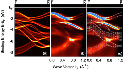
Figure 3. Comparison of the nominally even symmetry band structure (if one assumes that there is mirror plane symmetry along the  –
– line) obtained from DFT (a) and experiment using ARPES with the p-polarization geometry and 34 eV photon energy along the
  –
– line (b). A direct comparison is made on (c) with the DFT calculations superimposed on the experimental result.
Download figure:
Standard image High-resolution image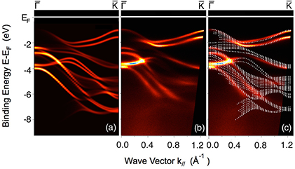
Figure 4. Comparison of the nominally odd symmetry band structure obtained from DFT (a) and experiment using ARPES with the s-polarization geometry and 34 eV photon energy along the  –
– line (b). A direct comparison is made on (c) with the DFT calculations superimposed on the experimental result.
Download figure:
Standard image High-resolution image
Figure 5. The experimental bulk WSe2 band structure obtained by angle-resolved photoemission spectroscopy for 75 eV photon energy along the high symmetry line from  to
to  for the nominally even symmetry (a) and odd symmetry (b).
Download figure:
Standard image High-resolution image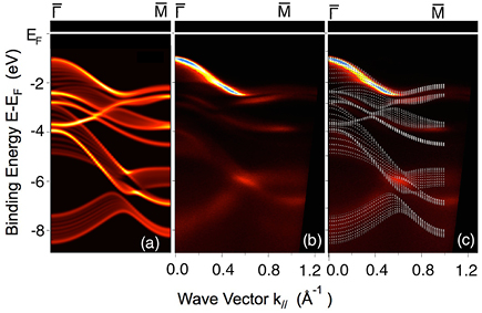
Figure 6. Comparison of the nominally even symmetry band structure obtained from DFT (a) and experiment using ARPES with the p-polarization geometry and 34 eV photon energy along the  –
– line (b). The direct comparison is made on (c) with the DFT calculations superimposed on the experimental result.
Download figure:
Standard image High-resolution image
Figure 7. Comparison of the nominally odd symmetry band structure obtained from DFT (a) and experiment using ARPES with the s-polarization geometry and 34 eV photon energy along the  –
– line (b). A direct comparison is made on (c) with the DFT calculations superimposed on the experimental result.
Download figure:
Standard image High-resolution image
In general the calculated band structures (figures 3(a), 4(a), 6(a) and 7(a)) agree well with experiment, as seen in figures 2(c), 3(c), 5(c) and 6(c), facilitating the assignment of various ARPES band spectral weight densities. The top of the valence band for bulk WSe2(0 0 0 1), at  , is best seen in the p-polarized photoemission geometry (figures 3(b), (c), 5(a) and 6(b), (c)). Thus the top of the valence band, in the vicinity of the center of the surface Brillouin zone, is dominated by even symmetry states along both the
  –
– and
and  –
– directions. Our DFT band structure calculations, as summarized in figure 2, predict that the even symmetry W
  weighted states dominate the top of the valence band at
  , in agreement with our symmetry assignment and results reported in [2, 4, 6, 12, 15]. This assignment is also consistent with the state symmetry assignment for the top of the valence band of MoS2(0 0 0 1) [27, 32].
At  , the W weighted bands are stronger in the s-polarization geometry (figures 4(b), (c) and 5(b)), and therefore contain odd symmetry states with respect to the
  –
– line. This is in agreement with our calculated symmetry dependent band structure, and with the results reported in [2, 4, 6, 12]. More explicitly, the WSe2(0 0 0 1) bands in the vicinity of the Brillouin zone edge near the
  point, near the top of the valence band, contain strong dxy (odd symmetry) contributions, as also found for MoS2(0 0 0 1) [27, 32]. As illustrated in figure 2, our DFT calculation shows that both W
  and dxy states are present at the top of valence band at
  (with 40%
  and 40% dxy). The W dxy (odd symmetry) bands are evident in the odd symmetry, or s-polarized photoemission geometry (figure 4(b)), similarly to the case of MoS2(0 0 0 1) [27, 32], in agreement with the predictions of earlier theoretical work [2, 4, 6, 12, 15]. Because the mirror plane symmetry is in fact absent along the
  –
– directions, the W 5
 (l = 2, m = 2) state contributions can hybridize with the W 5dxy (l = 2, m = −2) odd state contributions, adding W 5
 (l = 2, m = 2) state contributions to the top of the valence band near
  . Such a hybrid state, compatible with the dxy function along the
  –
– line, might be obtained by inserting
  and
and  (rotation about to the z axis of θ = π/6 (30°)), thus contains a mixture of dxy and
  [27]. Such an initial state would remain strongly enhanced in the s-polarization geometry, as is observed.
By comparing our calculated band structure components, shown in figure 2, and specifically the spectral weight densities attributable to the Se px and py states, with that obtained in our ARPES measurements, we conclude that the Se py weighted state is very strong in the experimental band structure in the odd symmetry photoemission geometry, compared to that of Se px in even symmetry, in the region of −2 eV. The W dxy bands are evident at the top of the valence band while W dyz are evident at somewhat larger binding energies along the  –
– line of the surface Brillouin zone, in the geometry that favors odd symmetry states (figures 4(b) and 5(b)). The Se px and py states are generally weak at the top of the valence band. This favors the observation of the even Se pz and W 5
 states (figures 3(b) and 5(a)) at the top of the valence band at
  but W
but W  and odd states like W dxy at the top of the valence band at
  (figures 4(b) and 5(b)), as we have noted above. The W dxz and dyz state contributions to the valance band structure are expected in the region of −2 eV at
  but it is the odd symmetry Se py and W dyz state contributions that are most evident in the experimental band structure (figures 4(b) and 5(b)). The Se px, py, W dxz and dyz state contributions to the valence band structure are expected in the region from roughly −4 eV going to −6 eV along the
  –
– line, as is seen in figures 3(b) and 4(b) respectively. There are additional bands evident, dispersing from roughly −6 eV going to −8 eV along the
  –
– line, of largely even symmetry (figure 3), containing Se pz and W s weight. It is Se pz and W s that dominates the bottom of the valence band.
The changes between the band structure taken at 34 eV (figures 3 and 4) and that taken at 74 eV (figure 5), while in many respects qualitatively similar at the top of the valence band, are the result of changing cross-sections and differences in wave vector normal to the surface (i.e. with respect to the bulk Brillouin zone). In fact, while the W 5d photoemission cross-sections fall quickly with increasing photon energy, the fact remains that the W 5d photoemission cross-sections are at least two to three times larger than the Se 3p [61], so an emphasis on the W weighted band is expected at modestly higher photon energies. Thus the bands at the top of the valence band for WSe2(0 0 0 1) along the  –
– are evident across the Brillouin zone (figure 5(a)) in the p-polarization geometry taken at 74 eV photon energy confirming that the top of the valence band must be dominated by the 5d wave functions with even symmetry with respect to the mirror plane, W
  and W
and W  , and the odd states like W dxy.
Our band structure calculations (figure 2), in agreement with [2, 4, 6, 12, 15], predict that the W  weighted states dominate the top of the valence band at
  across to
  , especially in the region of
  , in agreement with the even geometry ARPES experiments (figure 6(b)). This assignment is also consistent with the state symmetry assignment for the top of the valence band of MoS2(0 0 0 1) [27, 32]. There are additional band contributions arising from W 5dyz and Se py that appear to contribute strongly to the experimental band structure in the odd symmetry geometry in the region of −2 eV to −4 eV along the
  –
– line. We also note that along the
  –
– line, the Se py states appear strongly in the odd symmetry band structure (figure 7(b)) while the px states barely appear in even symmetry (figure 6(b)). A more pictorial representation of the state assignments, to various bands, is provided in the supplementary material (stacks.iop.org/JPhysCM/28/345503/mmedia).
Spin–orbit coupling
Figure 4(b) shows that the experimental WSe2 band structure along the high symmetry line from  to
to  has a large spin–orbit splitting,
  , of about 0.49 ± 0.1 eV at the top of the valence band at
  . At the Brillouin zone boundary, the splitting due to the spin–orbit coupling is the greatest at
  (figure 4) rather than
  (figure 6), as expected [1, 3–6, 8–12, 15, 23–25]. A previous study showed that bulk WSe2 had a spin–orbit splitting (fully explained by SOC symmetry considerations) of 0.45 ± 0.01 eV and 0.39 eV, in two different lower binding energy states below the valence band maximum, along the Δ high symmetry line of the bulk Brillouin zone, or along Γ to A, i.e. perpendicular to the (0 0 0 1) planes [5]. Other experimentally determined values for the spin–orbit splitting of the top of the valence band at
  , in the region of ~0.5 eV, have also been reported for bulk WSe2 [3, 4, 6], in accord with our experiments. Note that the experimentally determined 0.49 ± 0.1 eV spin–orbit splitting at the top of the valence band at
  for WSe2(0 0 0 1), obtained here, is smaller than the 0.51 ± 0.01 eV seen for monolayer WSe2 [24]. This is also in agreement with theoretical expectations of 0.47 eV [4] and 0.54 eV [8] and our calculated value of 0.48 eV. Table 1 summarizes a comparison of the values for the band splitting due to the spin–orbit coupling observed at the top of the valence band at
  for both the monolayer and bulk WSe2 for both theory and experiment. Although the top of the valence band for bulk WSe2(0 0 0 1) is seen to be at
  (the center of the Brillouin zone) rather than
  , as seen for monolayer WSe2 [24], the energy difference between the top of the valence band at
  and
and  is small.
Table 1. A compilation of the spin−orbit splitting, ΔSOC, at  , the energy difference between the top of the valence bands at
  and
and  (ΔΓ→K) and the effective mass at the top of the valence band at
  for the upper spin−orbit component (the branch closer the Fermi level) and for the lower spin−orbit component compiled from the literature for monolayer and bulk WS2.
| SOC (meV) | ΔΓ→K (eV) |
Effective mass at K (upper) | Effective mass at K (lower) | |
|---|---|---|---|---|
| Monolayer (expt.) | ~400 [16] | 0.2 ± 0.03 [2] | −0.35 ± 0.01 [24] | −0.49 ± 0.05 [24] |
| 400 [18] | 0.5 [14] | −1.4 ± 0.6 [2] | ||
| 404 [20] | <0.78 ± 0.02 [24] | |||
| 412 [21] | ||||
| 430 [22] | ||||
| 460 [17] | ||||
| 510 [19] | ||||
| 513 ± 10 [24] | ||||
| Monolayer (theory) | 463 [10] | 0.34 [11] | −0.36 [15] | −0.54 [15] |
| 456 [12] | 0.496–506 | −0.34 [25] | −0.35 [25] | |
| 462–466 [15] | [15] | −0.52 [23] | ||
| 461 [25] | 0.5 [24] | |||
| 454–469 [24] | 0.55 [2] | |||
| 501 [23] | 530 [12] | |||
| 500 [8] | ||||
| 630 [9] | ||||
| Bulk (expt.) | 490 ± 0.010 |
−0.07 ± 0.01 |
−0.41 ± 0.04 |
−0.43 ± 0.04 |
| 450 ± 10 [5] | −0.030 [3] | −1.05 ± 0.05 [6] | ||
| 500 [3] | −0.08 [4] | |||
| 500 [4] | −0.26 ± 0.0.2 [2] | |||
| 500 [6] | ||||
| Bulk (theory) | 480 |
−0.064 |
−0.37 |
−0.53 |
| 470 [4] | 0.018 [3] | |||
| 540 [8] | −0.224 [3] | |||
| −0.24 [2] |
aNegative values indicate  is the top of the valence band while positive values indicate that
  is the top of the valence band.
bThis work.
is the top of the valence band.
bThis work.
The hole effective mass at the top of the valence band at  is estimated from the experimental band mapping to be −0.41 ± 0.04 me, for the upper spin–orbit component (the branch closer to the Fermi level) and −0.43 ± 0.04 me, for the lower spin–orbit component. These results are consistent with the estimates of −0.35 ± 0.01 me, for the upper spin–orbit component (the branch closer to the Fermi level) and −0.49 ± 0.05 me, for the lower spin–orbit component, obtained from the experimental band structure of monolayer WSe2 [24]. Our calculations suggest that the hole effective mass values at the top of the valence band at
  for bulk WSe2(0 0 0 1) are −0.37me and −0.53me, respectively, generally in agreement with the experimental results.
Conclusions
We have used ARPES measurements and DFT calculations to study the symmetry-dependence of the band structure of bulk WSe2. Surprisingly, in spite of the overall low symmetry along the lines of the surface Brillouin zone of WSe2(0 0 0 1), even away from the high symmetry point  along the line from
  to
to  , we find that photoemission symmetry selection rules are generally applicable according to the symmetry of the various atomic orbital contributions as previously shown for MoS2(0 0 0 1) [27, 32]. For bulk WSe2, we find that a splitting of 0.49 ± 0.01 eV at the top valence band is due to spin–orbit coupling, in excellent agreement with the value of 0.48 eV calculated from DFT. This value is in the same range as that observed for monolayer WSe2. Any chirality of the states, as is observed with graphene [62], may also lead to photoemission of an even symmetry state in s-polarized light (nominally the odd state selection geometry), but is an unlikely dominant explanation for the results here. Spin–orbit coupling, as certainly exists in WSe2 at
  , has been implicated as a possible cause of this effect in graphene [63].
Acknowledgments
This research is supported by the National Science Foundation through grant NSF-ECCS-1508541 and by the U.S. DOE through grant DE-FG02-07ER15842. EFS acknowledges financial support from the JSPS postdoctoral fellowship for overseas researchers as well as the Alexander von Humboldt Foundation (Grant No. P13783). The experiments have been performed under the approval of HiSOR (Proposal No. 15-A-18). The DFT calculations were performed using resources from the National Energy Research Scientific Computing Center (NERSC, project 1996) and the Advanced Research Computing Center at UCF.