Abstract
The deposition of Mn on to reconstructed InSb and GaAs surfaces, without coincident As or Sb flux, has been studied by reflection high energy electron diffraction, atomic force microscopy and scanning tunnelling microscopy. On both Ga- and As-terminated GaAs(0 0 1), (2 × n) Mn-induced reconstruction domains arise with n = 2 for the most well ordered reconstructions. On the Ga-terminated (4 × 6), the Mn-induced (2 × 2) persists up to around 0.5 ML Mn followed by Mn nano-cluster formation. For deposition on initially β2(2 × 4)-reconstructed GaAs(0 0 1), the characteristic trench structure of the reconstruction is partially preserved even beyond 1 monolayer Mn coverage. On both the β2(2 × 4) and c(4 × 4) surfaces, MnAs-like nano-clusters form alongside the reconstruction changes. In contrast, there are no new Mn-induced surface reconstructions on InSb. Instead, the Sb-terminated surfaces of InSb (0 0 1), (1 1 1)A and (1 1 1)B revert to reconstructions characteristic of clean In-rich surfaces after well defined coverages of Mn proportional to the Sb content of the starting reconstruction. These surfaces are decorated with self-assembled MnSb nanoclusters. These results are discussed in terms of basic thermodynamic quantities and the generalized electron counting rule.
Export citation and abstract BibTeX RIS

Content from this work may be used under the terms of the Creative Commons Attribution 3.0 licence. Any further distribution of this work must maintain attribution to the author(s) and the title of the work, journal citation and DOI.
1. Introduction
The all-epitaxial combination of crystalline magnetic and semiconducting materials opens up many possibilities for engineering spintronic devices [1, 2]. The transition metal pnictides (TMPs) such as MnAs and CrSb, and Heusler alloys such as Co2MnSi, are very attractive for such applications. This is due to both their favourable magnetic properties (high Curie temperature and, in some cases, nearly 100% Fermi level spin polarisation [3–6]) and their compatibility with conventional III-V semiconductors using molecular beam epitaxy (MBE) [7–10]. This allows fully in situ growth of devices such as optical isolators [11] and spin light emitting diodes [12]. Secondly, III-V materials can be epitaxially overgrown on a manganese pnictide epilayer, allowing the flexible growth of ferromagnet/semiconductor multi-layers such as superlattices [13, 14] rather than just magnetic contact deposition. However, the behaviour of the interface between the TMP and the III-V semiconductor is crucial for successful spin injection. The Schottky barrier height (SBH) can also be better controlled by producing atomically sharp interfaces in MBE; for example, the MnAs and MnSb SBHs are different when these materials are grown on GaAs (1 1 1)A and (1 1 1)B faces [15] while MnAs/Si shows a low SBH of 0.16 eV [16] suitable for spin injection interfaces with a resistance-area product in the optimum range [17].
As well as control of the interface barrier heights, it is important that interface states with minority spin character do not arise around the Fermi level, which could reduce the effective spin polarization [18]. While TMP/III-V heteroepitaxy is well established, rather little is known about the detailed formation of interfaces. Ideally, the interface structure could be controlled with atomic layer precision but in practice this may be hampered by the presence of a surface reconstruction in the substrate layer (whether the III-V semiconductor [19] or the TMP film [8]). For example, while Mn pre-layers have been used in (non-MBE) growth of MnSb on GaAs [20], Mn deposition on to GaAs surfaces is known to lead to magnetic ordering and a change of reconstruction [21]. A second example is the growth of MnSb on GaAs versus InP or GaSb—sharp interfaces are readily formed on GaAs while on both of the latter substrates endotaxial growth occurs due to interdiffusion [22, 23]. Recent work has highlighted the importance of the initial substrate reconstruction in the growth of both Fe on GaAs [24, 25] and magnetic oxides on magnesia or alumina [26]. In the case of MnAs growth on GaAs(0 0 1), a complex and unusual initial growth phase is observed involving randomly oriented MnAs-like nuclei prior to epitaxial growth [27].
Monolayer surface structures of Mn on III-V surfaces are also of fundamental interest from the points of view of Mn incorporation (e.g. into dilute magnetic semiconductor [DMS] thin films), magnetic nanostructure formation (e.g. half-metallic atomic wires [28]), or fundamental magnetic interactions (e.g. anisotropic magnetic coupling via surface states [29]). For Mn growth on GaAs(0 0 1), quite complex kinetics have been inferred [30] during the transition from clean GaAs surface reconstruction to Mn-induced surface alloy reconstruction. A recent study of Mn on GaAs has highlighted the effects of As-rich versus As-poor surface reconstruction on the incorporation of Mn into GaAs interstitial or substitutional sites [31], which is important for optimising DMS performance [32].
During the initial stages of heteroepitaxy or atomic layer deposition on III-V surfaces, it is common for coexisting reconstructions and/or a surface alloy to form. A classic example is the wetting layer formed in InAs-GaAs heteroepitaxy [33] where reconstruction domains of the alloyed InGaAs layer may influence subsequent nucleation of three dimensional (3D) islands [34]. Such alloy surfaces frequently show incommensurate diffraction patterns in reflection high-energy electron diffraction (RHEED) [35] and so a local probe such as in situ scanning tunnelling microscopy (STM) is needed both to reveal nano-scale reconstruction domains [30, 34] and measure 3D island characteristics. Two- and three-dimensional structures often co-exist at the MBE growth front in the presence of epitaxial strain [36] and the evolving surface reconstruction is critical in understanding the growth mechanisms [37].
In this paper the interaction of Mn with a wide range of reconstructed InSb and GaAs surfaces is studied using RHEED, STM and ex situ atomic force microscopy (AFM). The formation of alloyed Mn-GaAs(0 0 1) reconstructed domains with (2 × n) periodicity [21] was observed, along with other co-existing GaAs reconstructions. In contrast, no alloyed Mn-InSb reconstructions formed on InSb, with Mn deposition instead destabilizing Sb-rich reconstructions to form MnSb nanoclusters. These results are discussed in terms of simple thermodynamic quantities and on the microscopic level within the generalized electron counting rule (GECR) framework [38]. The paper is structured as follows. Initially we describe the STM, AFM and RHEED results separately for InSb and GaAs, without detailed interpretation. Then we discuss and interpret the results with two themes. First, we explain the thermodynamics of the Mn-induced reconstruction changes including our interpretation of Mn-induced Sb removal on InSb. Second, we discuss the detailed reconstruction changes, concentrating on GaAs(0 0 1) and presenting a plausible model for the evolution of the surface incorporating both our observations and the results of other groups' work on this surface.
2. Experimental details
Experiments were carried out using two compact ultra high vacuum (UHV) chambers providing MBE capability with surface structure analysis. The Warwick MBE system is optimized for antimonide growth and the Sheffield system for arsenide growth. In both chambers, samples of size less than 10 × 10 mm2 are mounted on sample carrier plates. Both systems are equipped with retractable ionization gauges for measuring the beam equivalent pressure (BEP) and both are able to monitor the sample surface using reflection high energy electron diffraction (RHEED) throughout growth. Finally, each MBE system is connected to a UHV scanning tunnelling microscope (STM) to which samples can be moved for imaging. All images are shown in filled states at constant current (sample bias −3 V to −4 V, tunnel currents 0.2 nA–1 nA). The Mn effusion cells on both MBE systems were calibrated by direct BEP measurement and checked against MnAs or MnSb layer thicknesses measured by x-ray diffraction and electron microscopy. Epi-ready n-type III-V wafer sections (Wafer Technology Ltd, UK) were cleaned, loaded into vacuum and degassed using standard methods. In both chambers, Group III-rich surfaces could be prepared by either conventional ion bombardment and annealing (IBA) or wet chemical etching and annealing. Group V-rich surface preparation was restricted to the MBE system with the appropriate effusion cell (As or Sb). Substrate temperatures in both systems were measured by thermocouples calibrated to surface reconstruction transitions on GaAs and InSb (0 0 1) and to optical pyrometry.
After the desired starting surface had been prepared, Mn was deposited at a fixed substrate temperature of 300 °C (GaAs) or 280 °C (InSb) with coverages up to 2.4 ML (ML). Here one ML is defined as the surface atom density of GaAs(0 0 1) and is equal to 6.25 × 10¹⁴ atoms cm−2. The Mn flux was also fixed at the equivalent of 0.005 ML s−1 for continuous growth. This growth rate was effectively slowed in the vicinity of coverages at which reconstruction changes were expected to occur by using 4 s duration 'bursts' of deposition with growth interrupts. The RHEED patterns were monitored continuously throughout the Mn deposition cycles and transitions between patterns of different symmetries were noted carefully. At the substrate temperatures used, reconstruction changes due to vacuum annealing alone are slow (e.g. via Group V desorption) and so any changes of reconstruction could be attributed to the Mn flux. Once the evolution of the RHEED patterns had been established, samples were imaged using in situ STM after cooling in vacuum. For some experiments, the Mn deposition was also interrupted at various stages to image the surface using STM. On Mn/InSb samples where it proved difficult to image the surfaces at high resolution in STM, due to surface roughness and the presence of steep 3D island-related topography, samples were imaged outside UHV by AFM. An Asylum Research MFP-3D microscope was used in tapping mode to obtain the surface morphology on a wider scale than possible with STM and with greater tolerance to roughness.
3. Results
3.1. InSb
Three InSb crystal faces were investigated, with the starting reconstructions: c(8 × 2) and c(4 × 4) on InSb(0 0 1); (2 × 2) and
 R30° on InSb(1 1 1)A; (3 × 3) and (2 × 2) on InSb(1 1 1)B. These reconstructions can be separated into two distinct categories, namely In-rich and Sb-rich, as shown in table 1. The In-rich (0 0 1)-c(8 × 2), (1 1 1)A-(2 × 2) and (1 1 1)B-(3 × 3) surfaces are typically obtained by MBE growth under Sb-poor conditions or by IBA. They terminate at In atomic layers or elementally mixed layers. In contrast, the Sb-rich (0 0 1)-c(4 × 4), (1 1 1)A-
R30° and (1 1 1)B-(2 × 2) surfaces are obtained by growth under Sb-rich growth conditions or by annealing with incident Sb flux. These surfaces are terminated by Sb layers. These reconstructions could all be obtained with sharp and streaky RHEED patterns in the Warwick MBE system and examples of the Sb-rich RHEED patterns are shown in the upper panels of figures 1–3.
R30° on InSb(1 1 1)A; (3 × 3) and (2 × 2) on InSb(1 1 1)B. These reconstructions can be separated into two distinct categories, namely In-rich and Sb-rich, as shown in table 1. The In-rich (0 0 1)-c(8 × 2), (1 1 1)A-(2 × 2) and (1 1 1)B-(3 × 3) surfaces are typically obtained by MBE growth under Sb-poor conditions or by IBA. They terminate at In atomic layers or elementally mixed layers. In contrast, the Sb-rich (0 0 1)-c(4 × 4), (1 1 1)A-
R30° and (1 1 1)B-(2 × 2) surfaces are obtained by growth under Sb-rich growth conditions or by annealing with incident Sb flux. These surfaces are terminated by Sb layers. These reconstructions could all be obtained with sharp and streaky RHEED patterns in the Warwick MBE system and examples of the Sb-rich RHEED patterns are shown in the upper panels of figures 1–3.

Figure 1. RHEED patterns observed on the InSb(0 0 1) surface with the electron beam directed along the [1
 0] crystallographic direction showing transition from 2× [c(4 × 4) at θMn = 0 ML], to 1× [a(1 × 3) at θMn = 0.1 ML] and finally to 4× [c(8 × 2) at θMn = 0.35 ML]. Long (short) white lines indicate integer (fractional) order streaks, while the dashed boxes to the right show the reciprocal lattice region sampled in RHEED.
Download figure:
Standard image High-resolution image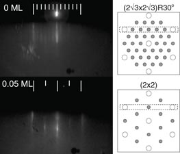
Figure 2. RHEED pattern observed on the InSb(1 1 1)A surface with the electron beam directed along the
 2] crystallographic direction showing transition from 6× [
R30° at θMn = 0 ML], to 2× [(2 × 2) at θMn = 0.05 ML]. Explanatory symbols are as figure 1.
2] crystallographic direction showing transition from 6× [
R30° at θMn = 0 ML], to 2× [(2 × 2) at θMn = 0.05 ML]. Explanatory symbols are as figure 1.
Download figure:
Standard image High-resolution image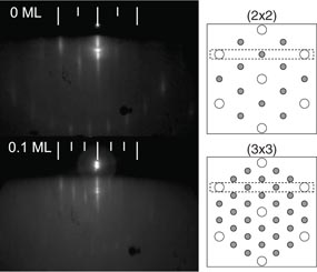
Figure 3. RHEED pattern observed on the InSb(1 1 1)B surface with the electron beam directed along the (
 2) crystallographic direction showing transition from 2× [(2 × 2) at θMn = 0 ML], to 3× [(3 × 3) at θMn = 0.1 ML]. Explanatory symbols are as figure 1.
Download figure:
Standard image High-resolution imageTable 1. Reconstructions and reported models for InSb and GaAs surfaces. The ideal elemental content is given in ML for the top layer(s) of the reconstruction.
| Surface | Reconstruction | Group III content (ML) | Group V content (ML) | Reference | |
|---|---|---|---|---|---|
| InSb | (0 0 1) | c(8 × 2) | 0.84 In | — | [45] |
| a(1 × 3) | — | 1.66 Sb | [57] | ||
| c(4 × 4) | — | 1.75 Sb | [58] | ||
| (1 1 1)A | (2 × 2) | 0.75 In | — | [59] | |
 R30° R30° |
0.50 In | 0.25 Sb | [60] | ||
| (1 1 1)B | (3 × 3) | 0.44 In | 0.22 Sb | [61] | |
| (2 × 2) | — | 1.75 Sb | [59] | ||
| GaAs | (0 0 1) | (4 × 6) | 1.00 Ga | 0.08 As | [40] |
| β2(2 × 4) | — | 0.75 As | [43] | ||
| c(4 × 4) | — | 1.75 As | [39] |
For all In-rich surfaces studied, deposition of Mn up to 1 ML coverage had no effect on the RHEED pattern, beyond slight degradation in the streak sharpness consistent with surface roughening, and sometimes very weak transmission diffraction features. In contrast, the Sb-rich surfaces were seen by RHEED to go through reconstruction changes at well defined and reproducible Mn coverages (θMn, in ML).
The RHEED patterns observed during Mn deposition on Sb-rich (0 0 1), (1 1 1)A and (1 1 1)B InSb surfaces are shown in figures 1–3 respectively. The (0 0 1) samples demonstrated two reconstruction changes. In the first, at low Mn coverage (θMn = 0.10 ML), the Sb rich (4 × 4) changed to a fainter a(1 × 3). This reconstruction persisted during subsequent Mn deposition up to θMn = 0.35 ML, where it transformed into a slightly spotty c(8 × 2). On the (1 1 1)A substrate the Sb-rich
 R30° surface changed to a sharp (2 × 2) reconstruction at a Mn coverage of θMn = 0.05. The InSb(1 1 1)B surface changed from the Sb-rich (2 × 2) to a (3 × 3) surface reconstruction at θMn = 0.10 ML. The transitions were all simultaneous with deposition, and not seen to change in the pauses between 'burst' doses of Mn. A brief period of mixed domains of the initial and subsequent reconstructions was observed close to the transition.
The relationship between the change of Sb content in the reconstruction ΔSb and the Mn coverage, θMn, is shown in figure 4 for the three InSb surfaces. The ΔSb values are taken from table 2, based on the layer-by-layer atomic contents in table 1. These values are not precisely defined since real surface reconstructions are not perfectly stoichiometric, e.g. the c(4 × 4) can accommodate top layer heterodimers, reducing its Sb content and increasing its In content [39]. Despite this, and the experimental uncertainty in the Mn coverage, there is a clear linear relationship between ΔSb and θMn. Furthermore, there is no indication of any surface reconstruction not characteristic of clean InSb, and all the transitions occur in the direction Sb-rich to In-rich.
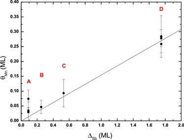
Figure 4. Amount of Mn required to trigger a reconstruction change on InSb (θMn) as a function of the change in Sb content of the top layer(s) of the surface reconstruction (ΔSb). The transitions are labelled A–D according to table 2.
Download figure:
Standard image High-resolution imageTable 2. Details of the transitions observed on the Sb terminated surfaces of InSb. ΔSb is defined as the Sb content in the reconstruction layers of the Sb rich reconstruction and the resulting reconstruction, whilst ΔIn is the corresponding change of In content in the reconstruction layers. The transitions correspond to the labels shown in figure 4.
| Transition | Surface | Transition | ΔSb | ΔIn |
|---|---|---|---|---|
| A | InSb(0 0 1) | c(4 × 4) → a(1 × 3) | −0.09 ML | −0.16 ML |
| B | InSb(1 1 1)A |
 R30° → (2 × 2) R30° → (2 × 2) |
−0.25 ML | +0.25 ML |
| C | InSb(1 1 1)B | (2 × 2) → (3 × 3) | −0.53 ML | +0.44 ML |
| D | InSb(0 0 1) | c(4 × 4) → c(8 × 2) | −1.75 ML | 0 ML |
Figure 5 shows the surface morphology of the Sb-rich c(4 × 4) and the In-rich c(8 × 2) surfaces using in-situ STM and ex-situ AFM. The STM images clearly show ML-height terraces and steps. While the c(4 × 4) has typically meandering terraces (figure 5(a)), c(8 × 2) surfaces have squarer terraces, higher step density and higher anisotropy (figure 5(b)). The surface morphology of the c(4 × 4) surface after 0.4 ML Mn deposition is shown in figure 5(c) and strongly resembles that of the clean c(8 × 2) surface, in agreement with the observed c(8 × 2) RHEED pattern. Typical AFM images for 1.00 ML of Mn on the c(4 × 4) and c(8 × 2) InSb(0 0 1) surfaces are shown in figures 5(d) and (e) respectively, together with height profiles across typical islands. Irregularly shaped islands with heights of approximately 30 nm and basal diameters ranging from 150 nm to 300 nm are found for Mn deposition on to the Sb-rich c(4 × 4), together with a much higher density of small 3D islands with heights (2–5) nm. In contrast to this bimodal island size distribution, Mn deposition on to the In-rich c(8 × 2) produces a lower density of quite uniformly sized islands, with heights around 50 nm and base diameters of 200 nm. It is straightforward to integrate the total volume in the island arrays and convert to ML equivalents. This yields island volume densities (total volume per unit area) of (1.92 ± 0.18) ML for the c(4 × 4) surface and (1.10 ± 0.06) ML for the c(8 × 2) surface respectively.
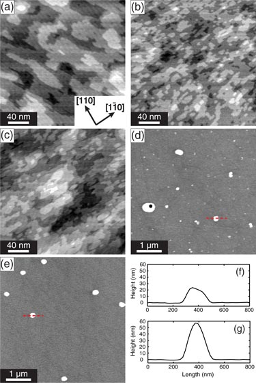
Figure 5. Surface morphology of InSb(0 0 1) surfaces prior to and following Mn deposition from in-situ STM (a)–(c) and ex-situ AFM (d)–(g). In (a) and (b) are shown the starting c(4 × 4) and c(8 × 2) surface morphologies respectively, while panel (c) shows an initially c(4 × 4) surface after deposition of 0.4 ML of Mn. The surface morphology and a typical island cross-section (dashed line) are shown for 1 ML Mn on (d) an initially c(4 × 4) surface and (e) an initially c(8 × 2) surface. Line profiles for large islands present on the c(4 × 4) and c(8 × 2) surfaces are shown in panels (f) and (g) respectively.
Download figure:
Standard image High-resolution image3.2. GaAs
The GaAs(0 0 1) surface has been studied with three different starting reconstructions: (4 × 6), β2(2 × 4) and c(4 × 4). From table 1 it can be seen that, analogously to InSb, distinct Ga- and As-rich reconstructions can be obtained by direct substrate surface cleaning or epitaxial growth. The broadly Ga-rich (4 × 6) reconstruction occurs following ion sputtering and UHV annealing without As flux (Warwick MBE), and is thought to have a complex sub-surface structure with surface heterodimers [40]. The As-rich surfaces are obtained through growth under As rich conditions and/or annealing under As flux (Sheffield MBE). The β2(2 × 4) reconstruction is the normal reconstruction during MBE growth, while the c(4 × 4) is an As-rich surface similar to that found on InSb(0 0 1) which may be present during low temperature MBE growth of Ga1−xMnxAs DMS materials.
The evolution of the RHEED patterns (not shown) for Mn deposition on the As-rich (2 × 4) and c(4 × 4) surfaces was more complicated than that seen on InSb surfaces. Unlike InSb, no simple trend from V-rich to III-rich reconstruction was observed with increased Mn deposition. On c(4 × 4), the fractional order streaks faded during Mn deposition leaving a (1 × 1) pattern, while on (2 × 4) starting surfaces a similar loss of fractional order streaks was observed along with increasing spotty transmission diffraction features. In both cases, half-order streaks were most persistent. On the Ga-rich (0 0 1)-(4 × 6) surface, the RHEED evolution was clearer (figure 6). The (4 × 6) periodicity clearly changes at θMn = 0.23 ML to (2 × 2), although hints of coexisting (4 × 6) remain. The transition is complete by θMn = 0.30 ML, at which the (2 × 2) pattern is sharpest. At larger Mn coverages the pattern begins to degrade and incommensurate transmission features are subsequently observed. As with the InSb surfaces, these transitions were simultaneous with deposition and persist between doses, i.e. the time dependence is weak.
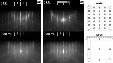
Figure 6. RHEED patterns observed on the GaAs(0 0 1) surface with the electron beam directed along the (a) [1 1 0] and (b) [1
0] crystallographic directions. The transition from (4 × 6) (bare surface) to predominantly (2 × 2) (θMn = 0.30 ML) is shown. Details are given in section 3.2 and the explanatory symbols are as figure 1.
Download figure:
Standard image High-resolution imageAFM images of the surface morphology for the GaAs(0 0 1)-(4 × 6) surface after Mn deposition (θMn = 1.25 ML) are shown in figure 7. At larger scan sizes (figure 7(a), 5 µm × 5 µm), the surface appears rather flat, with a low density of 3D islands present on the surface. At higher magnification (figures 7(b) and (c)) the presence of smaller 3D islands at high density is revealed. The islands are approximately 2 nm in height and 25 nm in base diameter. The volume density of material in these nano-islands is (0.82 ± 0.16) ML, although the volume integration for this surface is hampered because thresholding to obtain the background height of the substrate is more difficult.

Figure 7. Surface morphology from AFM of GaAs(0 0 1)-(4 × 6) substrate following Mn deposition. Scan sizes are (a) 5 µm × 5 µm and (b) 1 µm × 1 µm, also shown is a cross-section corresponding to the dashed line.
Download figure:
Standard image High-resolution imageThe As-rich (2 × 4) and c(4 × 4) surfaces were studied using STM and the images obtained for them are shown in figures 8 and 9, respectively. Figure 8(a) shows the clean (2 × 4) surface, with As dimer rows orientated along the [1
0] direction visible. Following deposition of 0.8 ML of Mn, figure 8(b), the original (2 × 4) structure has been disrupted and a co-existing (2 × n) structure develops. Some small islands are also visible on the surface. With increasing θMn (1.2 ML, figure 8(c)), the ordering of the (2 × n) improves and rod-like features form on the surface. The orientation of the rods is perpendicular to the As dimer row direction on the (2 × 4) surface. On this basis, and noting that Group III-rich domains of similar appearance in STM have been observed during InAs-GaAs growth in As-deficient conditions [41], these rods are attributed to Ga-rich reconstruction domains. However, we cannot rule out the formation of an alternative Mn-induced reconstruction. Finally, at high coverages of Mn (1.8 ML in figure 8(d) and 2.4 ML in figure 8(e)) the density and size of the islands increases. The number of Ga-rich domains also increases with periodicities ranging from (2×) to (6×) while the observed heights range from 0.2 nm to 0.6 nm. The height of the 3D islands is approximately 2 nm at θMn = 2.4 ML and they exhibit lateral extensions of greater than 40 nm. The formation of irregularly shaped islands and the presence of Ga-rich surface reconstructions indicates that As removal is taking place, analogously to Sb removal on InSb.
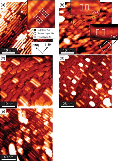
Figure 8. Morphology of the GaAs(0 0 1) surface from in situ STM, with Mn coverages of (a) 0 ML (initial β2(2 × 4)surface), (b) 0.8 ML, (c) 1.2 ML, (d) 1.8 ML and (e) 2.4 ML. Increasing Mn coverage results in a disordered (2 × n) structure (highlighted in panel (b) co-existent with the original (2 × 4) structure), with a meandering superstructure elongated in the [1
0] direction (b). This is followed (c)–(e) by the formation of irregularly shaped 3D islands and rod-like features elongated in the [1 1 0] direction. Inset in (a) is an expanded view of a β2(2 × 4) domain with atomic positions overlain.
Download figure:
Standard image High-resolution image
Figure 9. Morphology of the GaAs(0 0 1) surface from in situ STM, with Mn coverages of (a) 0 ML [initial c(4 × 4) surface, with inset expanded view and atomic positions overlain], (b) 0.8 ML, (c) 1.2 ML and (d) 1.8 ML. As on the (2 × 4) surface, increasing Mn coverage results in a disordered (2 × n) structure.
Download figure:
Standard image High-resolution imageThe c(4 × 4) surface follows the same general trends as those seen on the (2 × 4). STM of the clean surface is shown in figure 9(a), with the characteristic brickwork pattern of surface dimers clearly visible (an expanded view with atomic positions overlain is inset). The asymmetric nature of the dimers and the preparation conditions used suggest that this is the α variant of the c(4 × 4) surface and so consists of heterodimers [42]. At θMn = 0.8 ML, figure 9(b), the (2 × n) periodicity appears, although it is more disordered than for the equivalent Mn coverage on the (2 × 4) surface. At θMn = 1.2 ML, figure 9(c), the surface island density has increased in addition to a greater number of rods visible on the surface. Finally, at θMn = 1.8 ML (figure 9(d)), the surface has degraded substantially and features a large number of irregularly shaped islands. The size of the islands ranges between 1.5 and 2 nm at θMn = 0.8 ML, to between 2.5 and 4 nm at θMn = 1.2 ML. The behaviour of the islands and rod features on this surface is identical to those on the (2 × 4) surface, although a greater level of disruption is observed due to the higher As content of this surface.
One clear difference in morphology persists between the initial (2 × 4) or c(4 × 4) surfaces. Starting with the c(4 × 4), the surface morphology beneath the islands and rods is a rather isotropic patchwork of few-nm-sized islands by around 1 ML Mn coverage (figure 9(c)). Conversely, the (2 × 4) starting surface leads to a distinct pattern of meandering dark trenches elongated along the [1
0] direction (figure 8(d)). The average spacing along [1 1 0] between these trenches is about 3 nm (roughly an 8× spacing), indicating that about half the original (2 × 4) trenches have been preserved in some sense (originally the trenches comprised two absent As dimers and a pair of absent second layer Ga atoms [43]). One implication is that the Mn-induced surface structures can either fill the trench or leave it at least partly unfilled. Finally, it appears that the corrugation of the top layer of the more Mn-rich surfaces (beneath the Ga-stable domains) becomes lower, and is less than that of the starting (2 × 4) dimer-pair rows (figures 8(b) and (c)). This suggests less well defined covalent bonds and a more metallic character to the surface.
4. Discussion
4.1. Thermodynamics
All the reconstruction periodicities induced by Mn on InSb are characteristic of clean InSb and the observed transitions are all consistent with a reduction in Sb content in the surface layers. It is exceedingly unlikely that a sequence of reconstruction periodicities matching those of clean InSb would occur as a result of Mn surface alloy formation on all three faces studied. Therefore, the simplest explanation is that the main action of the Mn on the Sb-rich surfaces is removal of Sb from the reconstruction, in the process forming a new surface with a lower Sb content. The first transition on InSb(0 0 1) is from the c(4 × 4) structure to the a(1 × 3), a reconstruction associated with the c(4 × 4) but with a slight reduction in surface Sb, resulting in disordered top layer Sb dimers [44]. The second transition is to the c(8 × 2) surface, which is the In rich reconstruction and is terminated by 0.84 ML of In [45]. The process appears to be quite generic since similar transitions occur on the (1 1 1)A and (1 1 1)B surfaces. Indeed, the linear relationship between ΔSb and θMn (figure 4) suggests that the efficiency of Mn-induced Sb removal is similar on the three low index faces studied. The gradient of the line is 0.16, suggesting that one Mn adatom removes around 6 Sb atoms from the reconstructions at the substrate temperature of 280 °C. It is plausible that some Sb will desorb into UHV during the Mn deposition process but Mn atoms cannot desorb at such low substrate temperatures. Since the underlying reconstructions after Mn deposition are characteristic of clean In-rich InSb, we conclude that Mn is not incorporated into a two-dimensional (2D) surface reconstruction, and instead it forms 3D islands, as confirmed by AFM (figure 5). The post-Mn deposition RHEED patterns (figures 1–3) show faint transmission features on the InSb integer streaks, which is consistent with transmission diffraction through small 3D surface features. The volume density in the islands is significantly greater for the c(4 × 4) surface [(1.92 ± 0.18) ML] compared to the c(8 × 2) surface [(1.10 ± 0.06) ML], at 1 ML Mn coverage. This suggests that the 3D islands are nearly pure Mn for deposition on the c(8 × 2) surface, but during growth and Sb removal on the c(4 × 4) surface, Sb is incorporated into the 3D islands to give a composition close to stoichiometric MnSb. During MnAs growth on GaAs(0 0 1), Braun et al found RHEED evidence (powder-like diffraction rings) for randomly oriented clusters with MnAs-like bond length during nucleation at sub-ML coverage [22]. Since the film becomes epitaxial, these clusters must be mobile. It is plausible that similar mobile clusters develop during Mn deposition on Sb(As)-rich surfaces without Sb(As) incident flux, such that MnSb(As) nano-clusters can form and reconstruction domain changes can be mediated.
Models based on standard thermodynamic quantities have been successful in predicting interface reactivity and phase equilibria for various metal-semiconductor systems [46–48]. Some simple thermodynamic considerations can illuminate basic differences between Mn behaviour on Group III and Group V rich surfaces, especially for InSb where the difference is stark. The enthalpies of formation for relevant binary compounds are shown in table 3. The reaction enthalpy for conversion from an Sb terminated surface to an In terminated surface,
 , can be expressed as:

Table 3. Enthalpies of formation for relevant binary alloys and compounds.
| Compound | ΔHf (kJ mol−1) | Reference |
|---|---|---|
| InSb | −30.5 | [62] |
| MnIn | −11.0 | [63] |
| MnSb | −35.0 | [63] |
| GaAs | −71.0 | [64] |
| MnGa | −34.0 | [63] |
| MnAs | −65.0 | [63] |
| AuIn | −21.0 | [65] |
| AuSb | −13.0 | [66] |
Here ΔHSR is the energy difference between the In terminated and the Sb terminated crystal. Such surface reconstruction energies can be calculated from density functional theory (DFT), incorporating the allowed range of chemical potentials for one of the species of a binary material. Such DFT calculations have been performed over many years for a wide range of III-V materials (e.g. [49]). Typically, surface energy differences between reconstructions are up to 10 meV Å−2, or approximately (5–10) kJ mol−1. The ΔHSR term tends to drive III-V surfaces annealed in UHV towards Group III termination due to the higher volatility of the Group V component, i.e. we would expect a negative value for the Sb-to-In (or As-to-Ga) reaction.
Equation (2) shows
 for the formation of an Sb terminated surface from an In terminated surface:

Using the enthalpy values given in table 3,
 and
and
 . The reaction of Mn with an Sb terminated surface is exothermic and can occur spontaneously, while the reaction of Mn with an In terminated surface will not occur for any reasonable value of ΔHSR. This is consistent with the observed formation of hexagonal MnSb nano-particles in dilute In1−xMnxSb thin films without post-growth annealing [50, 51]. Note that the opposite process has been reported for Au deposited on to the InSb(0 0 1) surface, in which the In termination is changed to the Sb termination surface by addition of Au [52]. This difference in behaviour is also explained by equation (2) due to the higher stability of AuIn compared to AuSb (table 3).
The simple picture of the Sb-terminated surface being reactive with incoming Mn while the In-terminated surface is rather inert can also explain the difference in 3D island morphology for Mn-InSb (figure 5). The nearest-neighbour distance is larger on the starting c(8 × 2) surface as Mn adatoms are free to migrate a long distance to find a 3D island. On c(4 × 4), it is plausible that the bimodal size distribution arises due to an initially short migration length of Mn adatoms and/or or MnSb clusters on the Sb-rich surface (producing a large density of small, more Sb-rich islands) which increases as more Sb is stripped from the surface (allowing larger, more Mn-rich islands to form with longer nearest-neighbour distances).
The observed behaviour on GaAs is more complex due to the combination of As removal (island formation) and Mn incorporation (new surface periodicity). If one neglects Mn incorporation, the resulting enthalpy changes would be
 and
and
 . Therefore, the formation of MnAs on an As-rich GaAs surface is marginally favourable but the absolute value of the enthalpy change is well within the likely range of variation of ΔHSR. Conversely, Mn will not react with a Ga-rich surface to form MnGa, although Mn2As and MnGa are known to form by annealing thick films of Mn in contact with GaAs [53]. Of course, the incorporation of Mn into new (2 × 2) reconstruction domains cannot be described in a simple binary alloy model and so we now discuss reconstruction formation on GaAs and InSb.
4.2. Reconstructions
Various adsorption sites can be considered for Mn at III-V surfaces [30, 31, 38]. Perhaps the most crucial distinction is between interstitial and substitutional sites, since substitutional sites should favour Mn incorporation for the growth of DMS thin films. Ohtake, Hagiwara and Nakamura [31] studied the influence of initial surface reconstruction on Mn incorporation into GaAs and found that substitutional sites are favoured in group V-rich conditions since the surface stress from As dimers in the c(4 × 4) reconstruction can be partly compensated by bulk bond length strain of around 5% due to substitutional Mn. This contrasts with the less group V-rich (2 × 4) surface, on which interstitial Mn is preferred leading to a (2 × 2) reconstruction [31]. The local strain due to the incorporation of Mn on to a substitutional site is related to the preferred bond lengths of cubic (zincblende B3 structure) MnSb or MnAs, compared to the host semiconductor. Experimental as well as DFT-derived values for the lattice parameter of cubic MnSb are available [5], giving a bond length of 2.815 Å. This is much closer to the bond length of InSb (2.806 Å) than is the case for Mn in GaAs, resulting in a bond length mismatch of only 0.3% (InSb) compared to 4.7% (GaAs) [31]. Since the surface stress due to Sb dimers in InSb(0 0 1)-c(4 × 4) is also small [54] reconstruction-dependent tendencies for Mn to adopt either substitutional or interstitial sites are weak. Rather, the thermodynamic driving force towards MnSb formation dominates, as borne out by the repeatable behaviour found here on (0 0 1), (1 1 1)A and (1 1 1)B reconstructed surfaces.
Concentrating on GaAs(0 0 1), where the surface reconstruction does play a strong role, we note that Mn-induced (2 × n) reconstructions have been observed by several groups (n = 1 or 2). It has been suggested that the fundamental unit is (2 × 2) and that one-dimensional disorder in the [1 1 0] direction leads to the observation of (2 × 1) diffraction patterns [30]. Our results (figure 8) are consistent with this idea. The Mn-induced (2 × 2) reconstruction on an initially (4 × 6)-reconstructed surface has not previously been reported, and our results in concert with previous studies suggest that this (2 × 2) periodicity is quite ubiquitous on GaAs(0 0 1) under a wide range of deposition conditions and initial surface reconstructions. However, it appears that the initially (4 × 6)-reconstructed surface, in the absence of As flux, cannot accommodate more than about 0.5 ML Mn in the (2 × 2) phase, since 3D nano-islands begin to appear for coverages above about 0.4 ML (figure 7). The volume density of these islands is consistent with their composition being Mn, not MnAs. The structural motifs considered in previous work for Mn-induced reconstructions on GaAs(0 0 1) have principally involved As-terminated structures but Yang et al [38] report higher total energies (less stable) for the Ga-rich γ140 and β40−1 structures shown in their paper. For As-free Mn deposition on a Ga-rich GaAs substrate, either no alloyed reconstructions above about 0.5 ML Mn are sufficiently stable or the formation of stable reconstructions with high Mn content is kinetically hindered, hence Mn nanocluster formation occurs.
In the following discussion we focus on behaviour of the (2 × 4) and c(4 × 4) under Mn deposition. The GECR [38] has been proposed as a heuristic for narrowing the range of possible reconstructions in metal/III-V systems. Consideration of the relevant Pauling electronegativities suggests that Mn will act as a donor on both GaAs and InSb. The surface then reconstructs according to standard ECR principles with interstitial Mn providing two valence electrons to the structure without forming covalent bonds. Conversely, substitutional Mn is assumed to form tetrahedral covalent bonds but to still only contribute two electrons. As mentioned above, interstitial versus substitutional incorporation can depend on the initial surface reconstruction [31]. Substitutional Mn on Ga sites results in a deficit of 1 electron per Mn, while interstitial Mn adds 2 electrons per Mn. Compliance with GECR does not guarantee stability, which may be compromised by local strain, for example. Some extra considerations must be borne in mind. Strict GECR-compliance will likely become less important as the Mn content of the surface layer increases beyond 1 ML where MnAs-like metallic structures arise. Indeed, the c(4 × 4)-Mn surface identified in [31] is not GECR-compliant, and Yang et al calculated non-GECR-compliant (2 × 2) structures at 0.75 ML and 1 ML Mn coverages [38]. This is consistent with the reduced atomic corrugation observed in STM at higher Mn coverages. Additionally, the formation of new structures clearly may be kinetically limited as observed by Colonna et al [30]. In the absence of incident As or Sb flux in our experiments, and given strong evidence for As removal by incident Mn, the formation of new As-rich reconstructions is likely to be hindered. However, structural rearrangements may be mediated both by mobile MnAs clusters (for which diffraction evidence was found by Braun et al [22]) and by mobile Ga atoms liberated by erosion of the As-rich reconstructions [55].
For the c(4 × 4) starting surface, Mn can adopt third layer Ga substitutional sites [31]. However, in the absence of incoming As flux this appears to disrupt the As-on-As dimer structure of the initial reconstruction and by 0.8 ML coverage the c(4 × 4) has been replaced by a (2 × n) (figure 9(b)). The formation of large islands and Ga-rich reconstruction domains confirms that atoms are displaced from within the reconstructed surface. It is worth noting that the c(4 × 4)-(2 × 4) transition on GaAs(0 0 1) can be triggered by deposition of Ga at fixed temperature in static conditions, and that mobile Ga atoms are required to effect the transition under As flux [55, 56]. Clearly, migrating Mn atoms are able to break up the As-on-As dimer structure in a similar way. The degree of disorder on this surface makes it difficult to speculate further about the incorporation pathways of the Mn. Nonetheless the results highlight the significant structural rearrangement induced by incident Mn in the absence of coincident As.
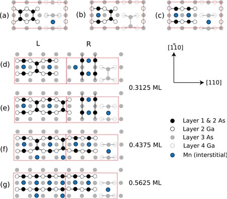
For the β2(2 × 4) surface the initial absence of As-on-As dimers suggests that interstitial Mn will be favoured [31]. Direct formation of both Ga-As heterodimers on an As atomic plane [31] and As dimers on As atomic plane [30] is likely suppressed by the lack of incident As flux in our experiment. This is supported by the observation of residual β2(2 × 4) domains co-existing with the same atomic plane terminating most structures (figure 8(b)). Hence the low coverage (0.25 ML Mn) dimer-on-As (2 × 2) reconstructions [31, 38] may not occur under the present conditions. Figure 10 shows plausible pathways to increasing Mn incorporation in an initially β2(2 × 4) GaAs surface which evolves towards a nominal (2 × 8) periodicity consistent with the observed (albeit highly disordered) structures. The (2 × 8) unit meshes shown are divided up into left (L) and right (R) (2 × 4) sub-units, with trench-filling occurring in the L sub-unit and a trench structure preserved in the R sub-unit. All the structures shown are compliant with GECR. For example, in structure (e), there are 28 As atoms (140 electrons), 14 Ga atoms (42 electrons) and 5 interstitial Mn atoms (10 electrons) giving a total of 192 electrons to distribute. Counting the different types of bonds, we have 44 Ga-to-As covalent bonds (taking 88 electrons), 10 As-to-As covalent bonds (20 electrons), 24 As dangling bonds (48 electrons), 24 As back-bonds (30 electrons) and 8 Ga back-bonds (6 electrons). Ga dangling bonds remain empty, hence the total number of electrons required is 192, providing charge neutrality.
Figure 10. Plausible GECR-compliant structure models for GaAs(0 0 1)-β2(2 × 4) under increasing Mn coverage in the absence of incident As flux. Atom types are colour coded in the figure. In (a)–(c) are shown Mn interstitial locations for (2 × 4) units at Mn coverages
 . Structures (d)–(g) are (2 × 8)-periodic comprising left (L) and right (R) sub-units, with associated Mn coverages given from
 –
–
 . These panels illustrate how (2 × 4) trench-filling could proceed with migrating Ga atoms and MnAs-like clusters, as described in the text. The (2 × 8) unit mesh boundary is slightly displaced to allow easier counting of the atoms and bonds.
Download figure:
Standard image High-resolution image
Initially, Mn can break As dimers in the top layer (a) or in the trench (b). Strain is induced by Mn in these planar interstitial sites [31, 38] so it is possible that local regions with high Mn density such as (c) with
 are destabilised. This induces the Mn atoms and As dimers to become a mobile MnAs-like cluster [22] and leads to the As removal observed here. The Ga-terminated structures remaining are not stable under GECR and form a source of free Ga atoms which can fill trenches in the β2(2 × 4). This allows the substantial structural rearrangement needed to form new structures with longer period along [1
0], observed in figures 8(b)–(d), along with Ga-rich reconstruction domains and larger 3D clusters. Such large-scale migration at these temperatures is consistent with the behaviour of GaAs during the (2 × 4)–c(4 × 4) reconstruction transition [55, 56]. It is very difficult to speculate about transient structures present during the local destabilization of the starting reconstructions and so we present the Mn-induced strain argument as a plausible mechanism which could be tested further by detailed DFT calculations. Such calculations have favoured planar interstitial Mn incorporation in the growing Mn-induced reconstructions in the absence of As-on-As dimers [31] and hence we use only this motif in figure 10, which does not attempt to explain the destabilization but rather the development of Mn-induced (2 × n) structures. The structures illustrated in figures 10(d)–(g) correspond to local Mn coverages from
are destabilised. This induces the Mn atoms and As dimers to become a mobile MnAs-like cluster [22] and leads to the As removal observed here. The Ga-terminated structures remaining are not stable under GECR and form a source of free Ga atoms which can fill trenches in the β2(2 × 4). This allows the substantial structural rearrangement needed to form new structures with longer period along [1
0], observed in figures 8(b)–(d), along with Ga-rich reconstruction domains and larger 3D clusters. Such large-scale migration at these temperatures is consistent with the behaviour of GaAs during the (2 × 4)–c(4 × 4) reconstruction transition [55, 56]. It is very difficult to speculate about transient structures present during the local destabilization of the starting reconstructions and so we present the Mn-induced strain argument as a plausible mechanism which could be tested further by detailed DFT calculations. Such calculations have favoured planar interstitial Mn incorporation in the growing Mn-induced reconstructions in the absence of As-on-As dimers [31] and hence we use only this motif in figure 10, which does not attempt to explain the destabilization but rather the development of Mn-induced (2 × n) structures. The structures illustrated in figures 10(d)–(g) correspond to local Mn coverages from
 . The left sub-unit labelled L undergoes trench-filling while the right sub-unit R maintains a trench-like structure. Filling could proceed by first the bonding of Ga in the empty trench sites [(d) L] using Ga liberated from erosion of destabilised dimer rows on which As-on-As 'split dimer structures' are formed [(d) R] akin to the γ202 structures of Yang et al [38]. Arsenic dimer adsorption on the filled trench can occur at the same Mn coverage [(e) L]. At higher local Mn coverage a continuous row of mixed As dimers and split dimers can form with a missing-Ga trench remaining ((f) and (g)). These illustrative structures are all GECR-compliant. Above
 the metallicity of the surface is likely to render strict charge neutrality less important. The wide range of structural motifs involved in these long-period structures clearly allows for the observed deviations from ideal (2 × 8) periodicity and meandering of the residual trench structure.
5. Conclusions
The deposition of Mn on to InSb and GaAs surfaces produces very different behaviours. These can be understood thermodynamically in the case of InSb, where there is a significant free energy gain from forming MnSb clusters using the excess Sb in the reconstructed surface layers, to leave an In-terminated surface. This may be a route to self-assembly of magnetic MnSb nano-structures confined to predetermined layers, for example as opposed to MnAs nano-clusters realisable throughout heavily Mn-doped GaAs films by controlled annealing. Of course, the simple thermodynamic argument does not explain why no Mn-induced surface reconstructions appear on InSb, and detailed DFT calculations would be welcome. The lack of surface reconstruction-dependence of the behaviour of Mn on InSb differs from the corresponding behaviour on GaAs, observed by Ohtake et al [31], where the As-rich c(4 × 4) favours substitutional Mn incorporation. The much better match of bond lengths for substitutional Mn in InSb compared to Mn in GaAs suggests that with suitable kinetics (MBE growth conditions) a high fraction of substitutional Mn in InSb could be achieved during co-deposition of Mn, Sb and In.
In contrast to InSb, new surface-alloyed reconstruction occurs on GaAs(0 0 1). As observed in several previous works, (2 × n) structures appear, with n = 2 for the clearest RHEED patterns. Unlike most studies reported to date, we are depositing Mn without a coincident As flux. Nonetheless, even on the initial Ga-rich (4 × 6) reconstruction and in the absence of incident As, a sharp (2 × 2) Mn-induced reconstruction appears, highlighting the ubiquity of this reconstruction periodicity. It appears that further Mn incorporation into the initially (4 × 6) surface does not continue beyond around 0.5 ML Mn due to the appearance of Mn nano-clusters. On initially (2 × 4) and c(4 × 4) surfaces, the Mn deposition destabilises the As dimer reconstruction leading to both new Mn alloyed (2 × n) reconstructions, Ga-rich reconstructed regions and MnAs-like nanoclusters. For both GaAs and InSb, the composition of the 3D nanoclusters has been inferred only from volume density measurements by STM and AFM. It would be interesting to examine these clusters further using ex situ magnetometry and x-ray diffraction, which would require the surface and nanoclusters to be protected from oxidation with an Sb or As capping layer. Finally, on GaAs the characteristic trench structure of the β2(2 × 4) is partially preserved with around twice the periodicity along [1
0] even after 1.8 ML Mn deposition, and GECR-compliant (2 × 8) single-trench structures are given with local Mn content beyond 0.5 ML. This work further illustrates how different deposition conditions can strongly affect both the surface structures and nano-clusters produced for the Mn/GaAs system.
Acknowledgments
labelackntThe authors are grateful for the technical expertise of R Johnston. This work was supported by EPSRC (UK) via Doctoral Training Grant studentships, a Post-doctoral Prize Fellowship (University of Sheffield) and research grant EP/K032852/1.