
Abstract
A combination of static and oscillating magnetic fields can be used to 'dress' atoms with radio-frequency (RF), or microwave, radiation. The spatial variation of these fields can be used to create an enormous variety of traps for ultra-cold atoms and quantum gases. This article reviews the type and character of these adiabatic traps and the applications which include atom interferometry and the study of low-dimensional quantum systems. We introduce the main concepts of magnetic traps leading to adiabatic dressed traps. The concept of adiabaticity is discussed in the context of the Landau–Zener model. The first bubble trap experiment is reviewed together with the method used for loading it. Experiments based on atom chips show the production of double wells and ring traps. Dressed atom traps can be evaporatively cooled with an additional RF field, and a weak RF field can be used to probe the spectroscopy of the adiabatic potentials. Several approaches to ring traps formed from adiabatic potentials are discussed, including those based on atom chips, time-averaged adiabatic potentials and induction methods. Several proposals for adiabatic lattices with dressed atoms are also reviewed.
Export citation and abstract BibTeX RIS

Original content from this work may be used under the terms of the Creative Commons Attribution 3.0 licence. Any further distribution of this work must maintain attribution to the author(s) and the title of the work, journal citation and DOI.
1. Introduction
As the field of ultra-cold atomic physics develops, it becomes increasingly important to be able to trap and manipulate atoms in potentials that are more complex than the standard, well established harmonic potential. For example, quantum correlations between atoms are greatly enhanced in low-dimensional systems and in lattices [1]. Flexibility and control of atomic potentials is also required in the context of matter wave interferometry, as recently demonstrated in experiments using double-well and annular potentials [2–4]. Adiabatic potentials provide a way to make increasingly flexible, complex, smooth and controllable potentials to meet these requirements.
In this Topical Review we aim to understand recent experiments with adiabatic potentials for ultracold atoms. We start in section 1 with an introduction to radio-frequency (RF) dressing [5, 6] (i.e. using an adiabatic basis), and we will see how the first RF 'dressed' atom traps (see [7, 3]) worked, and the significance of the resonant and off-resonant modes of operation. These early experiments, which are described in section 2, made flattened, quasi-two-dimensional clouds of atoms and were also responsible for the first successful coherent splitting of a condensate on an atom chip; we will look at both these configurations. In section 3 we show how a second RF field can be used both for characterising the potentials by spectroscopy and for carrying out evaporative cooling of adiabatically trapped atoms [8–10]. The dressed atom approach has been very successful as an approach to making ring traps for atoms [11–16], both theoretically and experimentally, and we will explore some of the possible configurations in section 4. We will also see how several types of cold-atom lattice potentials can be made in section 5 [17, 18]. Finally, in section 6, we present an overview of recent developments of adiabatic trapping using induction and the fields generated by induced currents [19].
1.1. Magnetic traps
Before looking at 'dressing' [20], we examine the individual components required: magnetic traps and magnetic resonance. The basic trapping of atoms with dressed states requires two components: a static magnetic field and a RF field. The Zeeman effect shows that spectral lines are split by the presence of a magnetic field. More importantly here, this means that the energy of a cold atom in a magnetic field depends on the field's absolute value. Figure 1 shows these energies as a function of the static field strength B0. It is clear that if we have a magnetic field that varies in space,  , we will have a potential that varies in space, too. Thus, pure magnetic trapping simply requires a magnetic field strength that varies in space; by arranging for a minimum in field strength, we obtain a trap for so-called weak field seeking states.
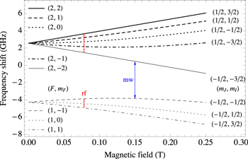
Figure 1. The energies of Zeeman split states of rubidium 87 as a function of magnetic field strength  . The red arrows indicate typical RF transitions between magnetic sub-levels at moderate magnetic fields and the blue arrow indicates a typical microwave transition (to be discussed in section 6). Most experiments are conducted in the 'weak'-field, linear regime on the left side of the figure.
Download figure:
Standard image High-resolution imageTo express this mathematically, we first note that the standard expression for the energy of the atomic dipole with a magnetic dipole moment  in a static magnetic field
  is given by

The magnetic dipole moment results from the electronic and nuclear contributions. For most of this review, we focus on the weak field part of figure 1 where there is a linear dependence of energy on magnetic field as given in equation (1). In this situation the projection of the angular momentum  is a good quantum number, and the atom has a magnetic dipole moment
  where gF is the Landé g-factor, and
  is the Bohr magneton. Taking the direction of the magnetic field
  at a location
  as the local quantisation axis, the projection of the angular momentum of the sub-state labelled mF is
  , and its energy in the weak-field regime reads

As an example, a static 3D quadrupole field, produced by a pair of coils with opposite currents, is described by a field

which has a gradient  in the x–y plane. This magnetic field configuration provides atom trapping at the origin with a potential
 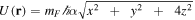 from equation (2) with
  . Such a quadrupole trap gives rise to losses by spin flips near the centre where the magnetic field vanishes (see e.g. [21–23]). A typical magnetic trap which avoids this problem is the Ioffe-Pritchard (IP) trap which has a non-zero magnetic field at its centre (typically produced by an additional coil). Its potentials will be found from equation (2) and are illustrated for F = 1 in figure 2.
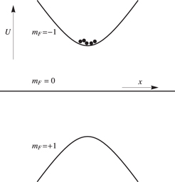
Figure 2. Schematic illustration of the energy levels in a magnetic trap for a total angular momentum F = 1 where there are three sub-levels. Only the  state is a trapping state in this configuration (corresponding to the F = 1 ground-state in rubidium where a negative gF reverses the order of levels compared to a positive gF). The filled circles indicate the location of atoms in the magnetic trap. Real numbers of atoms could typically reach 109 depending on trap type and preparation. The magnetic potentials shown are a 1D section through a typical Ioffe-Pritchard magnetic trap.
Download figure:
Standard image High-resolution image1.2. Dressed trap basics
Dressed traps can be formed for sufficiently strong RF fields near a region of magnetic resonance. (We will discuss off-resonant dressed trapping in section 2.2.) In basic magnetic resonance, the RF radiation couples to an atom through the interaction (1) involving a static magnetic field  and an oscillating magnetic field
  from a RF source. For the typical RF fields used, the electric dipole interaction is negligible. The location of the magnetic resonance is determined by when the RF photon energy
  matches the Zeeman splitting given by equation (2) (see also figure 1), i.e. resonance occurs in the linear regime when

where  is the local Larmor frequency. The Larmor frequency, with a factor of ℏ, is the separation between the magnetic states. The case of a IP trap is illustrated in figure 2, with a potential minimum for the upper state. For the case of a region with a linear gradient of magnetic field in the x-direction, we see a Larmor frequency which varies linearly in x in figure 3(a). At any position r, we can define a local detuning from resonance

Figure 3. Schematic representation of trapping in adiabatic potentials in one-dimension from the point-of-view of the bare and adiabatic states. (Upper panel): bare, undressed Zeeman energies shown as a function of position for a magnetic field with uniform gradient (compare with figure 1 where the x-axis is magnetic field strength). Magnetic resonance with RF radiation takes place at the location marked x0. An atom starting in the  state and moving from left to right would undergo a resonant transition at point x0 and end up in the
  state, following the thick lines. Example shown schematically for F = 1 in rubidium. (Lower panel): thick line: upper adiabatic potential shown for
  corresponding to the thick lines of the upper panel. In this case the resonance at x0 shows itself as a minimum in the adiabatic potential (with the Rabi frequency
  taken to be constant in this illustration). At the location of the minimum, the separation of the adiabatic potentials is given by
  , as in equation (11). Dashed lines: the other two, non trapping adiabatic potentials
  and
and  . Note that in the dressed atom picture, the adiabatic potentials in the lower panel belong to a manifold of dressed states [20].
Download figure:
Standard image High-resolution imageWe can suppose that  defines the local quantisation direction, i.e. the local spin z-direction such that the Hamiltonian for a stationary atom in the presence of static and oscillating fields is

Here  is the RF magnetic field, oscillating with angular frequency
  , and potentially varying in space according to the antenna and way the signal is generated. In the case of linearly polarised RF radiation, the Hamiltonian for the interaction of the RF field, assumed to be a cosine oscillation, with the spin is
where  is defined as the component of
  perpendicular to
  , and
, and  are the angular momentum raising and lowering operators:
  . The presence of
  ,
,  , and the factor two arise from the rotating wave approximation (RWA) where the counter-rotating terms are dropped [24]. The '±' and
  ' signs in equation (6) depend on whether gF is positive or negative, respectively. If we follow the standard treatment and change to an appropriate frame rotating at frequency
  in the same local basis, we obtain

where the '±' sign again depends on the sign of gF, and the Rabi frequency is

The dressed state potentials, or adiabatic potentials, are obtained by diagonalising equation (7) in the local basis (z in the direction of  ) to obtain, without further approximation

where the  label indicates the new, local basis, direction and we introduce the generalised Rabi frequency

which should not be confused with the resonant value  . In this way the dressed potentials are found to be
where  is, by analogy with mF, a label for the states in the adiabatic basis (the diagonal basis of equation (9), rather than the bare basis of equation (7)). As with mF,
  has
has  values from
  to F. These potentials are shown, for
  , for a uniform magnetic field gradient in figure 3 where there is a minimum in the upper adiabatic potential at the position given by
  in this case.
The diagonalisation of equation (7) corresponds, geometrically, to a rotation about the local y-axis by an angle  given by

It should be emphasised that the validity of the potentials (11) depend greatly on the underlying quantities changing slowly in space, and the full dynamics should include a kinetic term in the Hamiltonian which produces small velocity dependent terms in the adiabatic basis of (9): the validity of the approximation will be partially quantified in section 1.3. Not only can the detuning  change in space, but the Rabi frequency
  can, and the quantisation axis defined by the direction of
  can also change direction. The rate of relative change in all these quantities should be small compared to the generalised Rabi frequency
  for the dressed potentials (11) to be valid. That is, we require
  and
and  for time-dependent motion in the potentials (see e.g. [25, 26]).
We make a remark about the restriction to linear polarisation in equation (7). An equivalent description of the linear polarisation case is obtained by considering the oscillation to be divided into two circular components: one which rotates in the correct sense for magnetic resonance (which is anti-clockwise about z for a positive gF), and a term which rotates in the other sense and which is neglected in the RWA. Thus, if circularly polarised RF is directly applied with the same amplitude, correct alignment and in the resonant sense, the Rabi frequency is effectively doubled compared to equation (8). If the circularly polarised RF has the opposite sense and good alignment to  , the Rabi frequency is zero and if the polarisation axis of a circularly polarised field is at an angle ϑ to z, the Rabi frequency is
  . As mentioned above, the correct sense of rotation for good coupling depends on the sign of gF and this can be used to modify potentials in a state selective way (e.g. between F = 1 and F = 2 in rubidium 87 [27].) In the general unaligned elliptical case one needs to compute the projection of the RF field onto an aligned circular component [28] within the RWA.
Figure 3 illustrates a situation where, in one dimension, there is a linear gradient of the magnetic field strength in space with magnetic resonance at a particular point (x0). If, for a moment, we view an ultracold atom as a classical particle, we can see that if it is initially positioned on the lowest sub-level, to the left of x0 with little or no kinetic energy, it will subsequently roll down the slope until it reaches the region of resonance. At the resonance point, and provided the RF field is sufficiently strong, the atom will be adiabatically transferred to the upper state. However, if it continues moving rightwards on the upper state, it will slowly lose the kinetic energy it gained until it turns around and goes back through the magnetic resonance region. In this way the atom is trapped around a region defined by the location of the resonance: the net effect on the atom is to be confined in the adiabatic potential seen in the lower part of figure 3.
1.3. Semi-classical description with the Landau–Zener model
To get more insight into the concept of adiabatic trapping, it is useful to recall the Landau–Zener model [29, 30]. The model was initially defined for two-state (spin-1/2) systems where the time dependent potential has a linear dependence on time, i.e.

where the constant λ describes the rate of change of potential with time and the coupling V0 is assumed to be a constant. For an atom moving at an approximately constant speed u, the 1D constant λ is given by  where U(x) is the potential at distance x along the direction of motion.
The Landau–Zener model is one of the simplest two-state models with a non-trivial time dependent Hamiltonian. The model Hamiltonian does not contain a kinetic term but nevertheless it still accurately reproduces many aspects of the dynamics of an atom passing through the resonance region with a constant velocity. The model has been successfully used to study the dynamics of wave-packets in molecular potentials, (see for example [31]). The dressed state quasi-energies  are found by diagonalising the Hamiltonian (13) at each space point so that

Note that we recover the spin-1/2 Hamiltonian (7) and energies (11) written for the basic spatial adiabatic energies in the previous section. The adiabatic energies  are shown together with the bare (or diabatic) model energies
  in figure 4(a). Provided the coupling is sufficiently strong, or the speed of the atom is sufficiently slow, the atom will follow the adiabatic path. Because the model is analytically solvable [29–31], we can quantify the non-adiabatic behaviour. In the limit
  , the probability P of remaining in the adiabatic state (a 'red' path in figure 4(a)) is

where the adiabaticity parameter Λ plays a central role and is given by

We note in particular that the probability P above depends exponentially on the square of the coupling V0. This means that the adiabatic approximation is extremely good when Λ is rather larger than unity (e.g. for  ). Finally, note that the result (15) for a two-level system has been generalised to N equally spaced levels (e.g. when
  ) [32], where the modified result is
  for the probability of remaining in the adiabatic state. Further, in moving from the Landau–Zener model to realistic situations with cold atoms we change from a prescribed time-dependence (
 ) to one that is determined by the dynamics of the atomic motion. This means that an atom can accelerate to the Landau–Zener crossing point, or it can change its speed during the crossing, or it may not reach a crossing at all if it decelerates on an upwards potential. Nevertheless, we have found that when a crossing takes place, the Landau–Zener expression (15) works well, for a single crossing, provided that the classical velocity on the un-dressed potential is used at the crossing point [33]. However, for a more complete treatment of non-adiabatic effects for extended systems, this semi-classical trajectory-based approach should be replaced by a quantum model [22, 23, 28, 34] which, for simplicity, we will not consider here. In the following we will assume that the coupling is strong enough for the probability (15) to be very close to 1 and for the adiabatic potentials to describe correctly the dynamics.

Figure 4. Features of the Landau–Zener model in the regime where the adiabatic following is imperfect. This is used as a guide to estimate the requirements for adiabatic following in dressed traps. (a) Time-dependent energies in the Landau–Zener model: the diabatic energies  are given by the diagonal elements of equation (13), i.e.
  and
and  , and are shown in blue. The adiabatic energies given by equation (14) are shown in red and make an avoided crossing at time zero similar to a dressed atom trap with its avoided crossing, figure 3, lower panel, at location x0. (b) The time dependent behaviour for
  (and time scaled with
  ). We show the bare state probability
  , in the case where the system started in bare state 1. Thus, for
  the probability
  , and for
  the probability in the model approaches the value given by equation (15) which is indicated by the horizontal line 'LZ' for
  . For adiabatic trapping this probability should attain a value exponentially close to unity after the crossing region.
Download figure:
Standard image High-resolution image1.4. Adiabatic potentials: from RF-induced evaporative cooling to an atom trap
As an example of how adiabatic following can be viewed in the dressed atom picture, consider the situation of evaporative cooling. The standard method used to evaporatively cool atoms in a magnetic trap involves a RF field which is resonant at a location away from most of the trapped atoms, but still within range of the most energetic atoms [35]. The conventional picture is shown in figure 5(a) for an F = 1 case. Only the atoms reaching the resonance region are transferred to other sub-levels and lost from the trap (at A or  in figure 5(a)). Because the most energetic atoms are removed from the magnetic trap, the overall temperature of the trap is reduced when it rethermalises, provided the RF frequency change is slow enough. In figure 5(b) we view the same process from the dressed picture. Here the RF resonances are turned into avoided crossings when the Hamiltonian is diagonalised. The mapping of the result for the time-dependent Landau–Zener system onto a spatially varying system results from considering equations (11) to form the adiabatic potential. Provided the adiabatic picture is valid, and the atoms follow their adiabatic potential, evaporative cooling now clearly results from the finite depth of the lower adiabatic potential. Adiabatic following implies here that the kinetic coupling induced between the dressed states by the kinetic operator can be neglected. The energetic atoms which reach the top of the lower potential at A (or
  ) will thus escape the magnetic trap, bringing about the desired cooling. Should the potentials not be sufficiently adiabatic (see e.g. the analysis of [36]), the efficiency of adiabatic cooling is much reduced as, ultimately, energetic atoms are not out-coupled from the magnetic trap. Atoms would also make transitions to other
  states and subsequently cause losses from the magnetic trap through collisions. We note that the same potentials seen in figure 5(b) play an important role in the efficient outcoupling of an atom laser [37], where one wants to control the height of the barrier at A or
  , allowing atoms to escape with the aid of gravity.
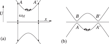
Figure 5. Different ways of looking at evaporative cooling in a magnetic trap. (a) Bare state picture: magnetic resonance takes place at A and  and removes the most energetic atoms. (b) Adiabatic state picture: the labels 'A' and
  ' now mark the top of the lower adiabatic potential. In evaporative cooling atoms with sufficient energy reach this point and bring about a cooling process. The points B and
  indicate where a resonant dressed atom trap appears in the adiabatic potential.
Download figure:
Standard image High-resolution imageThus adiabatic potentials can be useful as a way to visualise evaporative cooling. If we consider now the upper adiabatic potential, the same picture in figure 5(b) can be used to examine our first resonant dressed atom trap. In principle the location marked B (or  ) in the upper adiabatic potential is a trap for atoms (in 1D), provided the atoms obey adiabatic following.
1.5. Adiabatic potentials: a simple example of loading the atoms into a trap
There are now many configurations for dressed atom traps but, when proposing new types of trap, one question to be borne in mind is that of loading the new trap from a standard source of cold atoms, such as the original magnetic trap. In figure 5(b) this amounts to requiring the atoms to move from the minimum in the lower adiabatic potential to the minima in the upper adiabatic potential: a transfer requiring displacement in both position and energy. One solution [5–7] is shown in figure 6. The atoms start in a trap with weak, negatively (red) detuned RF which is ramped up in amplitude to create an off-resonant adiabatic trap (figure 6(b)). We note that this kind of negatively-detuned adiabatic trap was created with microwaves in [38, 39]. Once the trap is created, the frequency is steadily chirped, so that we pass through the resonance at the centre of the magnetic trap and extend the resonance points outwards (figures 6(c) and (d)). At the end of this procedure, figure 6(d), the atoms are loaded into the upper adiabatic traps at B and  in figure 5(b) (for details of this scheme see [6]). A weak point of this approach is that there is a moment between figures 6(b) and (c) where the potential is approximately quartic at the minimum leading to vibrational heating as the potentials evolve. We note that at this delicate point, in a situation when gravity goes in the x-direction shown in figure 6, the gravitational field prevents the appearance of a quartic potential, as in the case of the first experimental demonstration of a dressed RF trap [7, 40] (see section 2). In practice one can go a little faster here, and accept some non-adiabatic heating of the vibrational states of the trap with possible later cooling (see section 3 and [9]).
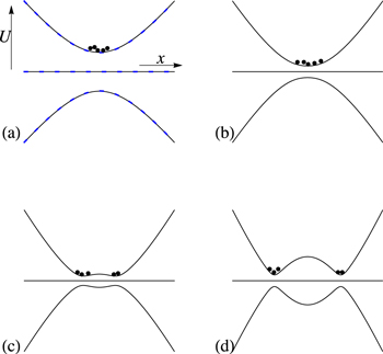
Figure 6. An illustrative sequence for loading atoms from bare states into dressed states, as proposed in [6]. (a) The blue dashed line shows adiabatic potentials with a very weak coupling and below resonance at the centre of the trap (F = 1). When the coupling is increased to its full value, the adiabatic potentials (solid line) show hardly any change because the RF is very off-resonant over the region shown in the figure. The black dots at the bottom of the trap symbolically represent the presence of the atoms. (b) The RF frequency is increased which moves the adiabatic levels closer together. This is because  is reduced in equation (11). (c) The RF frequency is further increased so that the bottom of the trap goes through resonance. (d) With further increases in frequency, a clear double-well potential appears. Note that if gravity were to act along the x-direction, the double-well structure may become slightly tilted.
Download figure:
Standard image High-resolution image2. First experiments
2.1. First experiments: bubble traps for atoms
In moving to the experimental realisation of resonant RF atom trapping, several important considerations need to be added. These considerations have some generality across the many different types of dressed trap and include the three-dimensional nature of the system involving vector fields, the effects of gravity, collisions and current noise. We describe these below, in the context of the first experiment, demonstrating trapping in RF adiabatic potentials.
First, the description in section 1.2 was essentially one-dimensional. However, in the context of magnetic traps there is a minimum of the magnetic field strength which means that, if the chosen RF frequency is higher than this minimum Larmor frequency, the location of the resonance will be a closed surface surrounding the minimum point. The effect is to rotate the one-dimensional picture of figure 5(b) in 3D resulting in a shell trap for the atoms: an egg-shell-like trapping surface, or bubble trap, as shown in figure 7. For the IP trap of figure 7 this shell is a prolate ellipsoidal surface; if the trap had been formed from the quadrupole field of equation (3), it would be an oblate ellipsoidal surface.
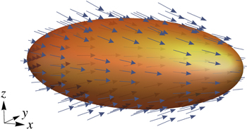
Figure 7. An 'egg-shell' surface for trapping atoms based on a typical Ioffe-Pritchard magnetic trap. The gold, three-dimensional ellipsoidal surface shows the location of magnetic resonance points, i.e. those locations where the strength of the magnetic field matches the RF frequency through equation (4). The vectors near the surface indicate the direction of the static magnetic from a typical Ioffe-Pritchard magnetic trap. In this example, because the static magnetic field has a dominant direction, a uniform field of linearly polarised RF radiation from an external antenna of axis y will have a polarisation approximately orthogonal to the static field (maximal coupling) over the surface of the ellipsoid. The ellipsoid shown has dimensions 100 μm × 10 μm × 10 μm and parameters of 100 G cm−1 for the gradient, 100 G cm−2 for the curvature along x, and a bias field of 1 G. The RF frequency is 703.5 kHz, corresponding to a resonant isomagnetic surface at 1.005 G.
Download figure:
Standard image High-resolution imageThe second important consideration is that, although atoms are in principle confined to the surface shown in figure 7, the vector nature of the electromagnetic fields also has to be taken into account. In the case of linearly polarised RF, the maximum interaction occurs when the vector  is perpendicular to the static vector field
  . Thus, if the static field changes direction around the egg-shell surface seen in figure 7, the adiabatic trap will be stronger or weaker (in adiabatic terms), depending on location. Since the minimum energy of the trap depends on the Rabi frequency (see equation (11) for
  , and the gap in figure 5(b)), an effect of this coupling inhomogeneity is that the potential energy of the bottom of the egg-shell varies around the surface of the shell. In the case shown in figure 7, based on a IP trap with a strong bias field, the relative direction of the RF and static magnetic fields changes little and the egg-shell has a fairly uniform minimum potential. However, in other situations, e.g. the quadrupole field distribution, there can be dramatic changes in direction which have to be considered (most especially during any loading sequence when the atoms may occupy relatively unusual locations).
The third important consideration is gravity. While atoms may be confined to an egg-shell such as figure 7, in the presence of gravity, only the lower part of the egg-shell may be occupied. An estimate of the importance can be gained by considering the thermal energy  in comparison to Mgh, where h is the height of the trap and M is the mass of the atom. For extremely small egg-shells, atoms might be distributed around the egg-shell, depending on the level of coupling inhomogeneity mentioned above. More typically, for ellipsoidal surface traps with larger radii, the atoms fall to the bottom, as can be seen in figure 8. This figure shows the first experimental demonstration of dressed RF trapping [7] and the first adiabatic trapping in the resonant regime. It is clearly seen that, as the RF frequency is increased to the highest value shown (bottom panel in figure 8), the atoms occupy the lower portion of an ellipsoidal surface with larger radii, resulting in less curvature and a downward shift of the atomic cloud. The loading scheme used was similar to that described in section 1.5 and [6]. Systematic results for the downward shift of the cloud, due to the increasing distance where magnetic resonance is located, were presented in [7] and [41].

Figure 8. Images from the first realisation of a resonant dressed RF atom trap. Taken with permission from [7]. The images show a sideways view of atoms at approximately 5 μK in a Ioffe–Pritchard type of trap with RF dressing in the two lower panels. The Rabi frequency is  . (Top) Initial distribution in the trap, without dressing; (middle) RF dressing field with frequency 3 MHz; and (bottom) dressed trap with RF frequency of 8 MHz. In the lower two panels the atoms are seen in the bottom of a shell (or bubble) trap.
Download figure:
Standard image High-resolution imageThe dressed atom can be regarded as being in a superposition of all the bare states (see figure 5(b)), as presented in [41]. This means that when two dressed atoms collide in an adiabatic trap, it is arguable that the spin states will change in a way that selects untrapped adiabatic states, resulting in rapid trap loss [42]. In practice this does not happen; the dressed RF traps in [7] had lifetimes for atoms as long as 30 s. The reason is that, to a good approximation, it is the local basis that matters for the colliding atoms. In the local basis the loading process ensures that  , equation (11), has an extreme value (it is a maximum stretch state) and, as a result,
  can not change when two such atoms collide [43]. The validity of this approach is assured for atomic speeds such that the collisions take less time than the RF period.
Our final practical consideration is the current noise leading to fluctuations in both the static magnetic field and the RF field. Current noise in a simple magnetic trap is known to lead to heating of the atoms [44]. For a dressed trap, this kind of current noise can shift the location and affect the harmonic frequency of the dressed trap. The resulting dipolar heating was investigated for dressed RF traps in [45], where it is found that DC current supplies and RF synthesisers generally meet the needed requirements. Heating rates below 2 nK s−1 per RF antenna and trap lifetimes longer than two minutes were observed in [46], which allowed the preparation of a quasi-two-dimensional quantum gas in a dressed trap and the study of its dynamics [46–48].
Current noise, and rather fast loading of the dressed trap both lead to some heating of the atoms. In section 3 we will examine two approaches that can be used to cool the dressed atom traps to counteract these effects where necessary.
2.2. First experiments: atom chips and double-wells for interferometry
RF dressed atom traps have played an important role within the framework of atom chips [49, 50]. In 2005 it was shown that a Bose–Einstein condensate (BEC) could be coherently split under an atom chip by using RF-induced adiabatic potentials [3]. Later this was followed by other experiments splitting condensates and observing interference effects with RF double-well potentials [51–56] or microwave double-well potentials [57]. Historically, atomic ensembles were first split apart on atom chips with magnetic hexapole fields [58, 59]. However, there were difficulties in atom chip development for matter–wave interference because the condensates used in matter–wave interference are located very close (tens of micrometres) to the chip surface and thus to the current carrying conductors. The currents in those conductors do not, in reality, take idealised straight-line paths, but actually meander on a microscopic scale [60]. In addition there is Johnson noise from the electrons [61] which can have a component resonant with trap excitations. The overall effect of these issues is, firstly, to cause a spatial break up of a BEC into pieces, and secondly to destroy the coherence of a BEC. The dressed-RF atom trap provides a controllable way of splitting the condensate into two coherent pieces in a way which strongly eases these two problems through its use of superposition states which protect the condensate [3]. The related issue of smoothing wire roughness with alternating currents is discussed in [62, 63].
Many of the atom chip experiments used dressed potentials in a resonant configuration, as described for the ellipsoidal surface traps above, or in an off-resonant configuration, or both. In the off-resonant configuration, the spatial dependence of the adiabatic potential comes about from the spatial variation of  ,
,  and the spatially dependent angle between them, resulting in
  in equation (11). For the production of double-well potentials, the resonant case can lead to a practical separation of tens of microns, and the non-resonant case allows separations of a few microns only, which is useful for atomic interference experiments. (We note that the non-resonant case has also been used to create anharmonic distortions in magnetic traps, to manipulate the vibrational states and have coherent control of trapped atoms [64–67].) The typical configuration starts with a Z-wire (or similar) magnetic trap [49], which typically results in a very elongated magnetic trap. There are many variants of this type of trap design (see e.g. [49, 68]) of which the Z-wire case is just one simple example where a current carrying wire is laid out on the surface of a chip in the shape of an opened out 'Z', i.e. as
  In figure 9(a) we see the long DC wire in cross-section through the centre of the 'Z', i.e. the current I is flowing into the drawing (in the negative z-direction). An approximate (2D) magnetic quadrupole field is set up by means of a bias field at 45
 to the chip surface, as shown in figure 9(a). This bias field cancels the field from the wire at the centre of the quadrupole. There would be a 'hole' in the trap at the centre of the quadrupole, where spin-flip losses could take place, but an additional uniform bias field (not shown) is applied in the z-direction, which plugs this 'hole' and results in an elongated magnetic trap. Then the dressing field can be applied to this magnetic trap with additional wires supplied with RF current: the example set-up, shown in figure 9(a), has a single RF wire for this purpose. At the location of the quadrupole, the RF field appears to be along x and parallel to the component of the static field in the x–y plane, but the coupling never vanishes because of the longitudinal z component of the bias field. In the non-resonant configuration a double well potential with a separation of a few micrometres is created because of the inhomogeneity of the coupling with the linearly polarised
  [69]. Note that in this non-resonant situation, the non-zero value of the detuning increases the generalised Rabi frequency, see equation (10), which helps to satisfy the adiabatic condition with respect to the resonant case.

Figure 9. Figures taken from [3] for an atom-chip experiment that produces a double-well potential and matter–wave interference fringes. (a) The atom-chip set-up with just two wires (one RF and one DC). The bias field at  forms a local quadrupole field at the location shown under the RF wire. A double well potential is formed due to the spatial variation in strength and direction of the RF field. (b) Image of interference fringes from the overlap of the two expanded clouds, i.e. from the release of the atoms from the two potential wells. (Reprinted by permission from Macmillan Publishers Ltd: [3], copyright (2005).)
Download figure:
Standard image High-resolution imageIn this way, by ramping up the Rabi frequency, a condensate can be coherently split into two pieces. To show that this splitting is done coherently, the two pieces could be put back together again. In [53] a split condensate is recombined by reducing the RF frequency to change a double-well potential back to a single-well, and in [70] a recombination is made with a sudden dip in Rabi frequency. However, to simply demonstrate coherence in splitting, it is straightforward to turn off the trapping fields and let the two condensates expand until they overlap. An example is shown in figure 9(b) where the expansion of the atom cloud reaches length scales rather larger than the initial separation. With the two clouds overlapping, imaging will show interference fringes which will be in the same location when the experiment is repeated [3, 51, 54].
Note that a larger separation can also be obtained by ramping up  to frequencies larger than the Larmor frequency at the trap bottom, in a resonant adiabatic potential configuration [3]. Atom chips can also be used with dressed microwave potentials to create double-wells and to split waveguides [57, 71, 72].
3. Spectroscopy, evaporative cooling and holes in dressed RF atom traps
In this section we consider the effect of a second RF field in the presence of adiabatically trapped atoms involved with a first RF field. There are two purposes for the second RF mentioned here. Firstly, a weak field can be used as a spectroscopic probe of the dressed atom trap: it can quantify the Rabi frequency and provide location information on the atoms. Secondly, as remarked above (section 1.5), we note that the process of loading an adiabatic trap can be one that creates excitations in the trap (although they could be minimised in some cases through optimal control techniques [73]). For this reason it may be better to load and then complete cooling, rather than trying to keep everything cold during a loading process. The standard technique for final stage cooling is evaporative cooling, which is often done with RF radiation in a magnetic trap as described in section 1.4. So it seems natural to try and use RF radiation to cool a dressed-atom trap. However, RF radiation is already used to form the dressed RF atom trap and it has to be understood how a second, cooling RF field might interfere with a dressing RF field.
In the next section we discuss the structure of the potentials with two RF fields, based on the work of [9], followed in section 3.2 by a discussion of spectroscopy in an RF trap. Then in section 3.3 we discuss evaporative cooling of dressed traps (both by using the second RF field and by using the spatially dependent Rabi frequency, without any second RF field). Also, in the following sections 3.1–3.3, to avoid confusion,  (and not
  ) and
) and  refer to the RF frequencies of the first and second RF fields, and
  and
and  refer to their respective Rabi frequencies.
3.1. Resonant surfaces with a second RF field
To gain some insight into the features introduced by a second RF field, we start by looking at the situation with a first RF field ( ) in the bare basis, such as used in figure 3 for a linear magnetic field (top figure for bare state picture ) or figure 5(a) for a quadrupolar or IP type of field. Figure 10(a) shows the latter case in 1D with this first RF resonance indicated with the grey arrows. This first field is resonant at two locations because the magnetic trap potentials separate from a minimum in the centre of the figure. These two 'grey' resonances actually result from a section through the egg-shell of resonance in figure 7. Taking the case of
  for the second RF (blue arrow in figure 10(a)), it is perfectly arguable, that for a strong enough Rabi frequency and very different RF frequencies, separate RF induced adiabatic potentials should be formed at (two) different locations to the
  resonance, defined by positions
  .
.
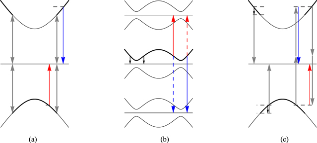
Figure 10. RF resonances with two RF fields. The horizontal axis represents position and the vertical axis indicates potential energy for the atoms. The effect of gravity is not included for generality and simplicity. (a) Bare magnetic trap potentials for a 87Rb F = 1 atom in a model Ioffe-Pritchard trap (adapted from [9]). The model potentials are harmonic at the trap bottom, but become linear for larger distance. The frequency  is the main dressing frequency (grey), and the states connected to the trapping adiabatic potential are underlined in bold. An additional RF field is added with frequency
  either below
  (red) or above
  (blue). For clarity only one of the four possible arrows indicating resonance is shown in the red and blue arrow cases: the full picture would have couplings just as shown by the grey arrows. (b) Adiabatic dressed potentials with three selected manifolds are shown for the first dressing field
  , with the locations
  of the
  resonance indicated. As explained in [9], additional resonances (with different couplings) appear at new positions
  with a Larmor frequency
  symmetric with respect to
  . The additional resonances are shown by the dashed lines for the two cases
  (red dash) and
  (blue dash). A direct resonance at position
  corresponding to the adiabatic level splitting also appears, as indicated by the short black arrows. (c) Bare potentials, but with the new resonances of (b) decomposed into multi-photon processes involving one or two dressing photons. The dressing photons are shown in grey as in (a), but with a single arrowhead indicating absorption or stimulated emission.
Download figure:
Standard image High-resolution imageHowever, if we look at the same situation in the dressed basis, figure 10(b), and now consider the second RF photon energy, it seems remarkable that in this picture the resonance with the second RF is only on one side of the dressed RF trap. That is, in this picture we might expect to see blue arrows at four locations. The dashed blue line in figure 10(b) shows the alternate resonance for the right-hand adiabatic potential well. Understanding this is important as figure 10(b) shows exactly the situation required for understanding a trap spectroscopy, or RF evaporative cooling, of a dressed RF trap.
This situation of 'extra' resonances was explored in [9] through the use of a 'doubly-dressed' basis. This approach is particularly effective when the picture given in figure 10(b) is valid, i.e. when the second dressing field is rather weaker than the first dressing field. In that case an approximate, effective adiabatic Hamiltonian is found which determines the coupling and energy of the second dressing field coupling to the first dressed system. If we denote, as in equation (5), 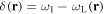 as being the first RF field detuning at location
  , and
, and  as the generalised Rabi frequency for the first RF field as in equation (10), then the resonance conditions are given by

with respective effective Rabi couplings [9]
We have used the angle θ given by equation (12), i.e.  .
.
For each resonance condition, there are in fact two resonant points on either side of the  resonance [9], shown as coloured solid and dashed arrows around the dressed minimum in figure 10(b).
At a large detuning  from the first dressing field,
  , we find that the resonance points are approximately given by

with the respective couplings [10]

In this limit, the first coupling given in equation (20) above is the expected Rabi frequency  seen with the solid coloured arrows in figures 10(a) and (b) (being either red, or blue, depending on whether
  , or
, or  , respectively). However, for the second coupling in equation (20) we see that, because we are in the limit
  , this second coupling is much reduced. This agrees with the picture given in figure 10(a), where the second resonance is not visible. In fact, though, as
  approaches
  , the two couplings become less unequal and also approach each other, in agreement with figure 10(b) [9].
The last condition for resonance in equation (19) is suggestive of the multiphoton interpretation of resonances, illustrated in figure 10(c). Looking first at the right-hand side of figure 10(c), there is a set of three resonances indicated in the bare basis (i.e. as in figure 10(a)). Left of the main resonance is a process involving the absorption of two  RF 'dressing photons' and the emission of an
  photon. This higher order process seen in figure 10(c) corresponds to the location of the blue dashed line in figure 10(b) and is, of course, in addition to the first order processes seen in figure 10(a). A similar argument applies to the red-dashed resonance which can be decomposed as the third order process, involving the emission of two
  RF 'photons' and the absorption of an
  photon for the case
  , seen at the far right of figure 10(c).
Finally, we draw the reader's attention to the short black arrows indicated on the left side of figures 10(b) and (c). These arrows indicate the locations of a low frequency resonance at  where transitions are directly stimulated between adiabatic states in the same manifold (figure 10(b)). The low frequency resonance can also be viewed in the bare basis as occurring via multiphoton processes (figure 10(c)) i.e. from a dressing photon
  plus, or minus, the low frequency photon energy. The low frequency resonance has been experimentally observed with dressed atoms [8, 10]; see the next section.
3.2. Spectroscopy of the dressed trap
In practice, the 3D situation makes the simple picture given above incomplete. We will explore this with figure 11 for the case of a dressed quadrupole trap shown in 2D cross-section. In figure 11(a) we see two resonant surfaces either side of the main trapping surface (marked with a dashed line). Only very energetic atoms will reach these two surfaces because of the tight trapping transverse to the trapping surface. For  (
( ), the dominant surface with stronger coupling is the outer (inner) surface. In off-resonant spectroscopic probing we start to pick up a tail of the distribution of the atoms, see figure 11(e). We could also perform evaporative cooling in this regime. As the frequency
  approaches
  , the surfaces eventually meet at the bottom of the dressed trap in figure 11(b). This is because the Rabi frequency is stronger at the bottom of the trap in a quadrupole trap with linear and horizontal RF polarisation in the y-direction. For figure 11(b) the condition
  is met at the trap bottom. At this point, in a spectroscopy measurement, the trap will be quickly emptied, indicating that the bottom of the trap has been located. This method can be used to determine accurately the local Rabi frequency in the trap. The Rabi frequency is slightly reduced as one climbs the sides of the atom trap and, for this reason, the surfaces meet on the sides of the trap, figure 11(c), only when the RF frequency
  is closer to
  than the value of
  at the trap bottom, to match the Rabi frequency at those locations. In a spectroscopic measurement there is still some atom loss (i.e. a signal) as some thermally excited atoms can reach the bottom of the second RF resonance surfaces. However, this is typically a narrow regime in
  , as seen in figure 11(e).
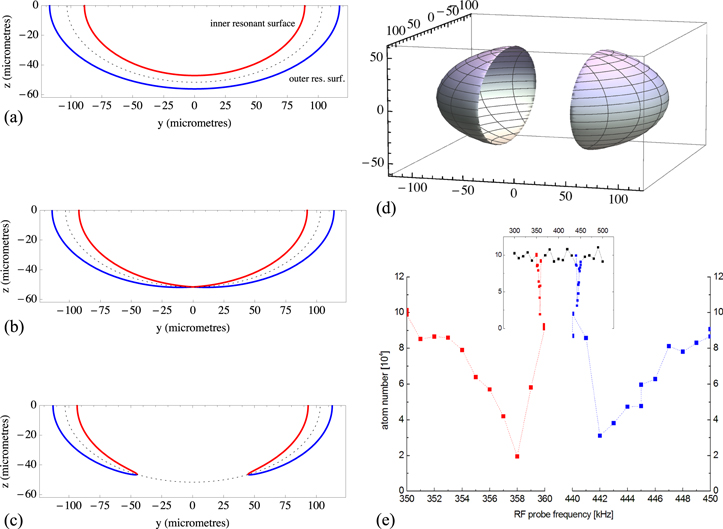
Figure 11. Figure showing resonances, or evaporation surfaces for a dressed quadrupole atom trap, with a linear RF polarisation along the y-axis. In (a)–(c) the dashed line indicates the location of the first dressing field resonance in this 2D section through the magnetic trap. The solid lines indicate the location of the second RF resonance in three situations: (a) second RF frequency  above resonance at the dressed trap bottom as in figure 10; (b) second RF frequency coincident with the first dressed RF trap bottom; (c) second RF frequency too low for the first RF trap bottom, but still resonant at higher locations because of the reduced Rabi frequency in the trap when z is increased. In all cases (a)–(c), both surfaces contribute to the spectroscopy signal. (d) Visualisation in 3D of the outer evaporation surface shown in (c). (e) Corresponding second RF spectrum (inset shows the full spectrum). The two peaks appear around
  . The minima occur at resonance at the trap bottom. The low (high) frequency wing of the lowest (highest) frequency spectrum correspond to the case (a), the central wing corresponds to the case (c). For all these plots, the magnetic gradient of the quadrupole trap is
  G cm−1 in the horizontal directions, the dressing frequency is
  and the Rabi frequency at the trap bottom is
 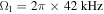 , as deduced from the spectra. Data from LPL.
Download figure:
Standard image High-resolution image3.3. Evaporation via high and low frequency resonances and via 'holes'
For evaporative cooling it is generally desirable to start with a RF frequency resulting in resonances away from the location of the atoms, as in figure 11(a) or (c), and then adjust the frequency so that the evaporation resonance surface approaches the atoms. The second RF can then remove the most energetic atoms and cool the gas to very low temperatures: see for example [14, 46].
One can also directly address the gap between the dressed states with a low frequency field. At the minimum point, this means applying a second RF field with a frequency equal to the Rabi frequency of the first RF field. In this situation, the minimum point of the trap is addressed and the atoms will empty out. However, if the low RF frequency is somewhat above the Rabi frequency, evaporative cooling can be performed, as demonstrated in [10] and reported in [8, 74]. Evaporation can be maintained by reducing the RF frequency to approach the Rabi frequency.
The low frequency resonance can be used for spectroscopy, as outlined in section 3.2 above. However, for evaporative cooling, rather than spectroscopy, it can be desirable to use a fairly strong second field to ensure the hot atoms are out-coupled adiabatically. Non-adiabatic transitions lead to the population of different  states which either are not trapped or lead to collisional losses [36, 43]. For the direct transition, where
  , the Rabi frequency
  is modified by an approximate factor
  [10]: thus the coupling is somewhat reduced and we note it is also optimal for aligned RF and static fields.
Finally, we note that it is possible to perform evaporative cooling without a second RF field [75]. In this case we can use the fact that for a quadrupole field, and for RF linearly polarised in a horizontal direction, the Rabi frequency varies hugely around the resonant ellipsoid: there will always be locations around the circumference of the ellipsoidal surface where the Rabi-frequency vanishes. These locations are places where the dressed trap 'leaks', i.e. atoms can escape. But since these 'holes' are located high up on the sides of the ellipsoid, at the equator for a horizontal linear polarisation, only the most excited atoms can reach the hole and escape. Thus, we can implement evaporative cooling using this feature, as was reported in [75], although this evaporation through two holes is expected to be less efficient than an evaporation through a whole resonant surface [76]. To adjust the cooling and reduce temperature the holes can be lowered by controlling the RF polarisation (using elliptically polarised RF).
(We note briefly that the holes could also be closed by using a rotating circular polarisation [77] which is a variant of a TAAP, a time-averaged adiabatic potential, see section 4.3.) This same kind of evaporation was used in a double well TAAP in [78].
4. Dressed ring traps
Ring traps for atoms have considerable interest, for example, as a geometry for excitations and solitons in quantum gases [79], as a way of pinning a vortex [80], and as an instrument for Sagnac interferometry [81]. In this context atom chips are of interest because they may lead to the creation of compact devices. However, a conventional atom chip approach would be to create a circular waveguide based on steady currents and magnetic fields such as in [82]. This is based on the idea that with current flowing down several long parallel wires on a chip surface, a magnetic 2D quadrupole field can be created away from the chip surface [83]. To trap atoms in a circular waveguide, one simply bends the parallel current carrying wires into concentric loops. However, a weakness of the single circular magnetic waveguide is the end effects associated with how the currents are brought into and out of the waveguide loop [84]. The potential issues, where currents enter and exit a waveguide ring, include distortion of the circular symmetry and the introduction of local bumps or dips in the waveguide potential.
In this section, and in section 6, we will see a number of techniques using dressed atom traps that avoid this problem and create smooth and symmetric ring traps for ultra-cold atoms.
4.1. RF egg-shell with optical assist
In 2006 Morizot et al [11] published a proposal for a ring trap for atoms based on the intersection of two types of potential for ultra-cold atoms. First, an 'egg-shell' potential from a 3D quadrupole magnetic field dressed to resonance is used. Since 3D quadrupole fields have an axis with higher gradient (because of Maxwell's equations3 ), this steeper gradient is arranged to be vertical, so that in the x–y plane a circular cross-section is obtained. Then the egg-shell system is overlaid with a blue-detuned optical potential formed from vertical standing waves of light (a 1D optical lattice). The intersection of these two potentials forms a set of ring potentials, stacked above each other, with different radii, see figure 12(a). Blue-detuned light was proposed to exclude atoms from regions of light and reduce photon scattering in the trap. For practical values of parameters [11], the trapping frequency in the vertical direction (optical confinement) is higher than in the horizontal direction (RF confinement). For example, in [11] a 430 μm diameter ring had a radial frequency of 1.1 kHz and a vertical frequency of 43 kHz. Indeed, the frequencies can be sufficiently high to reach a low-dimensional regime for a 1D, or 2D, quantum gas. A simple loading scheme was proposed which involved starting with the dressed RF atoms in the egg-shell trap, applying the blue-detuned standing wave of light to trap the atoms in a plane at the bottom of the egg-shell, and then shifting the RF trap downwards in position to open out the ring [11]. (This latter step can be accomplished by applying a bias field to shift the quadrupole field downwards.) The scheme was realised in [12], but with the standing wave of light replaced by two sheets of light. Reference [12] also demonstrated a novel variation of the loading scheme in which a blue detuned sheet is applied first before the RF radiation. This is used to push the atoms away from the zero region of the quadrupole trap as the RF is turned on. The ring trapping scheme of [11] has also been realised with light sheets in [85].
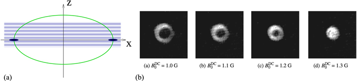
Figure 12. (a) Schematic showing the original concept of the hybrid RF/optical ring-trap. A ring of atoms is confined by the RF egg-shell potential radially (with minimum marked in green), and vertically by a blue-detuned optical standing wave (shown in blue). Figure adapted from [11]. (b) Images, taken from above, from the experimental realisation of the system shown in (a), but with just two sheets of blue-detuned light [12]. The different cases show different vertical bias fields which have the effect of moving the eggshell potential vertically, thus changing the ring diameter. (Figure 12(b) reproduced from [12] under a CC-BY 3.0 license.)
Download figure:
Standard image High-resolution image4.2. Atom chip approach to ring traps
At the start of section 4, we mentioned that conventional atom-chip ring traps, based on purely magnetic waveguides (without dressing), can have issues with their circular symmetry and local bumps or dips in the waveguide potential where currents enter and exit the waveguide structure. One approach to resolve this is to use induction methods (see section 6). Another approach uses two-phase RF currents [15, 69] to make 2D rings (or tubes in 3D). Figure 13(a) shows the chip with two RF wires on the underside. By adjusting the phase difference between the currents of the wires, the character of the proposed dressed trap can be changed significantly. The underlying magnetic trap is formed from DC currents in all three wires shown in figure 13(a) with appropriate bias fields in the z and vertical directions. The bias field in the z-direction ensures a functional magnetic trap in all three directions. The bias field in the vertical direction shifts the magnetic trap to the correct vertical position. Then, as the lower panel of figure 13(a) shows, RF currents which are equal amplitude, but in-phase, or π out of phase create a double-well potential in the 2D plane shown. When the currents are  out of phase, there is either a trap not unlike the original magnetic trap, or a ring-trap in the 2D plane shown. In this latter case, the conventional orientation of atom chips (horizontally, with the atoms underneath) means that the 'ring' belongs to a vertical plane, a bit like a car tyre, i.e. with a horizontal azimuthal axis. So, for the ring to be fully populated with atoms, it should either be very small, or there should be compensation of gravity from a Rabi coupling gradient [16], or an additional potential, such as an optical gradient (or a tilt of the chip). The depth of the ring in the (horizontal) z-direction in figure 13(a) is determined by the length of the current carrying wires on the chip and the method used to confine the atoms in the z-direction. In [15] the confinement was proposed to be formed by shaping the RF wires and the width was just a micrometre or so. In general, there are limitations to this approach because large rings will require large currents to place the magnetic linear quadrupole away from the chip surface; the part of the ring near the chip surface may be influenced by significant deviations from quadrupolar due to the proximity of the three wires and the finite width of the nearest current carrying wire, changing the local magnetic field direction.

Figure 13. (a) Atom chip scheme from [15] with the capability to produce a ring trap with its (x–y) plane perpendicular to the chip surface. An approximate linear quadrupole field is formed from DC currents in all three chip wires. RF currents with a phase difference δ flow down the outer chip wires. In the case  , a ring trap is produced. The cases
  produce double-well potentials in the x–y plane and the case
  produces a single potential well in the x–y plane. This scheme was realised in [16]. (b) Atom chip scheme from [27] which can produce a ring trap with its plane parallel to the chip surface. A 'ring' quadrupole is formed from ring-shaped permanent magnets ((b), left). It is not necessary to plug the centre of the quadrupole field because, under the right conditions, the dressing forms a trapping region away from the circular path of the quadrupole centre. The RF is applied from two circular coils (panel (b) right) which can have RF currents with amplitude and phase differences. Double ring traps and toroidal traps can be formed from this set-up. (Figure 13(a) reprinted with permission from [15], Copyright (2006) by the American Physical Society. Figure 13(b) reprinted with permission from [27], Copyright (2007) by the American Physical Society.)
Download figure:
Standard image High-resolution imageFigure 13(b) shows a different approach taken from [27]. In this case the ring potential will lie in a horizontal plane and the underlying magnetic trap is formed from two ring-shaped and concentric permanent magnets that provide a 'linear'-type quadrupole field with a zero that runs around the path of the ring trap. As a magnetic waveguide this trap would leak atoms from the centre but, by turning on the dressing field, the degeneracy at the bottom of the trap is lifted. In the simplest case, the RF field is generated by a pair of external Helmholtz coils which are operated out of phase to generate, in general, an elliptically polarised RF field. In the plane of the trap, the field can be arranged to be circularly polarised with respect to a quantisation axis which varies around the circle at the centre of the quadrupole field so that it is tangent to the ring (see figure 13(b) (right panel)). This creates a uniform coupling around the ring. Then a dressed-RF trap minimum occurs when magnetic resonance takes place away from the centre of the ring quadrupole and around a surface following the zero field centre: i.e. trapping takes place on the surface of a torus. By deliberately creating an imbalance in the currents in the external coils, an elliptical polarisation can be generated which results in a double-well potential around the ring: i.e. two ring traps are formed which, for the correct RF current parameters, can be above each other [27]. A Sagnac interferometer is proposed using this scheme in [86].
4.3. Time averaged adiabatic potentials (TAAPs)
The technique of obtaining new potentials by means of fast oscillations of other potentials is well established. The Paul trap for ions [87] works by periodically inverting an unstable saddle-point potential to obtain a stable trapping potential for certain trajectories. The TOP trap [88] (time-orbiting potential) is a magnetic trap for neutral atoms where a lossy field-zero point which is vulnerable to spin-flips is time-averaged away to make a well-behaved atom trap. The general principle is that the time-dependent motion, or oscillation, should be much faster than the mechanical motion of the atom or particle in the time-averaged potential. The same approach can be used with adiabatic potentials to create an even greater variety of trapping geometries [13]. The proposal to make a ring trap this way involved the time-dependent motion of an ellipsoidal surface trap (or more specifically, a dressed 3D quadrupole field with the strongest field gradient to the vertical). If a uniform vertical bias field is applied, the centre of the quadrupole field is simply shifted and, as a result, the surface potential is also shifted vertically. By applying an oscillating bias field, i.e. a bias field oscillating at a frequency much less than the RF frequency, or the Rabi frequency of the dressing field, the ellipsoid is essentially shaken vertically up and down. Two extrema of the motion, labelled t1 and t2 are depicted in figure 14(a) with dashed lines indicating the ellipsoidal surface trap location. The time-averaged potential minimum is dominated by the time spent in these extremal locations, and especially at their intersection. Thus, the time-averaged potential minimum is close to the intersection, and the full calculations show that a ring trap is formed (with an isopotential surface shown in figure 14(b)).
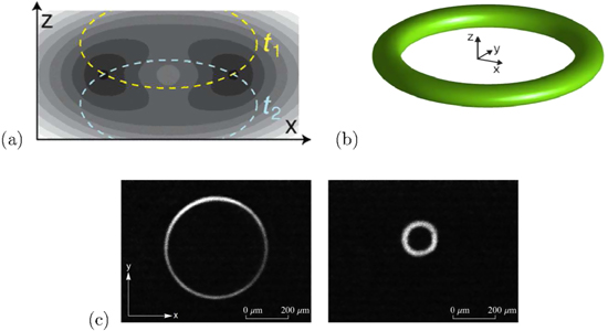
Figure 14. (a) Concept of a TAAP ring trap (time-averaged adiabatic potential ring trap). The trap is formed by time-averaging a vertically oscillating RF shell trap which is seen in (a) in a section across a diameter of the ring with contours showing the time-averaged potential. (b) A 3D isopotential surface for the time averaged potential produced by the vertical oscillations of the bubble shown as dashed lines in (a). (c) Experimental results for atoms trapped in a TAAP ring trap. The atoms are viewed from above in (c) with an absorption image. (Figures 14(a) and (b) reprinted with permission from [13], Copyright (2007) by the American Physical Society. Figure 14(c) reprinted with permission from [14], Copyright (2011) by the American Physical Society.)
Download figure:
Standard image High-resolution imageThese time-averaged adiabatic potentials (or TAAPs) have considerable potential for variable geometry and one can drive the trap in several directions as a function of time [13], as well as modulating the RF amplitude and frequency [89]. One should bear in mind that the driving has to be faster than the mechanical motion of the atoms (i.e. faster than the vibrational frequencies) and yet it should also, as mentioned above, be less than the Rabi frequency and the RF frequency. In addition, care has to be taken with exotic geometries to avoid any RF holes due to polarisation (section 3) where atoms could be lost.
The TAAP was first realised experimentally in [14] with some quite large and well defined rings (see figure 14(c)), and in [89], even larger, mm scale rings were formed for Sagnac interferometry. In addition to rings, we note here that a double-well potential was experimentally formed with a TAAP in [78, 90], and the versatility of TAAPs was demonstrated in [78] where, as well as demonstrating evaporative cooling, a vortex array was created in the TAAP. The whole vortex creation process in [78] was engineered with time-dependent adiabatic potentials.
5. Dressed lattice traps
Artificial lattices have been of importance in atomic physics for some time [91]. They have allowed the investigation of previously unseen condensed matter models and play an important role in the development of atomic clocks [92]. To date the lattices investigated have been optical lattices; typically a retro-reflected beam creates standing waves with periodic light shifts of energy levels.
RF dressed lattices offer different parameter ranges, such as the possibility for sub-optical-wavelength lattices. The first theoretical proposal is essentially an extension of the trapping concept of figure 3 to multiple RF frequencies [18], and even beyond the two frequencies considered for spectroscopy or direct evaporative cooling of an RF trap (section 3). Figure 15(a) shows how the lattice is built by having multiple magnetic resonances with many RF fields. In fact we can see from figure 15(a) that every lattice site generated requires two unique RF frequencies. Provided the underlying magnetic fields were linear in the one-dimensional space, the RF frequencies would approximately belong to a frequency comb if a regular lattice is desired. In that case, the lattice spacing is approximately determined by the frequency comb spacing and the magnetic field gradient. That is, for a lattice spacing d and field gradient  , the frequency spacing of RF fields is
  . The result of a detailed calculation of the potential (which has to account for the cumulative off-resonant shifts of the multiple RF fields on each other's resonance points), is shown in figure 15(b). One notes, however, that many RF fields are required to make a long lattice and that the lattice described is a 1D lattice. In the proposed variant of [93], a RF square wave produces the harmonics, but the decreasing amplitudes of those harmonics means that the 1D lattice is less effective as one travels out from the centre. In [94] three 1D potential wells are proposed to be produced with six RF frequencies. The potential wells are moved in space by controlling the RF frequencies in time. In this way it was possible to modify the tunelling rates between the wells for the controlled and efficient transfer of population between them.
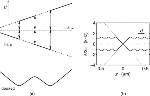
Figure 15. (a) Lattice trap schematic using multiple RF frequencies in the spirit of figure 3. Detailed calculations include 'light' shifts where one RF resonance shifts the location of another. (b) Taking the coupling into account, the lattice proposal of [18]. (Figure 15(b) taken with permission from [18].)
Download figure:
Standard image High-resolution imageIn our second example of rf dressed lattice physics the dressing field is applied to atoms already in an optical lattice. This results in a 2D dressed lattice which has been observed experimentally [17]. The optical field is necessarily off-resonant, as shown in figure 16(a), and has a well chosen laser wavelength between the D1 and D2 lines of 87Rb.

Figure 16. Hybrid dressed optical-RF 2D lattice in the experiment of [17]. (a) Relevant energy levels of 87Rb involving the off-resonant coupling of the F = 1 ground state to the D1 and D2 lines. The 35.90 MHz RF is only resonant with the  states because of the nonlinear Zeeman effect. (b) 2D lattice potentials for
  (top) and for the upper adiabatic state (bottom) at two Rabi frequencies: 20 and 205 kHz. (c) RF dressed state potentials for Rabi frequencies of zero, 20 and 205 kHz. (Figure 16 is taken with permission from [17].)
Download figure:
Standard image High-resolution imageThe light shifts in the F = 1 ground state of rubidium are very roughly equal and opposite in the  sub-levels with only small shifts in the mF = 0 state (see figure 16(c), top). The resultant 2D optical lattices are depicted in figure 16(b) (top). For the RF interaction, the bias field
  and the RF field
  are uniform in space and the bias field is sufficiently strong that we enter the nonlinear Zeeman effect regime and, in this case, the RF effectively forms a two-photon transition between
  and mF = 1 (figure 16(a), bottom, shown exaggerated). By mixing these optical potentials it is possible to form new structures on a sub-wavelength scale, as shown in figure 16(c) (bottom). These potential structures include lattices of ring traps [17]. RF dressed optical potentials have been further studied in [95, 96] (and we note a scheme for optically dressed sub-wavelength lattices was proposed in [97]).
Finally, we mention the proposal for lattices to be created with arrays of wires on an atom chip. In [98] an array of current carrying wires produced a 1D diffraction grating for atoms where magnetic-field zeros were plugged with RF potentials. However, a 2D RF dressed lattice which can trap atoms has also been proposed in [99, 100] (see figure 17). It is based on a double-layer atom chip with two perpendicular sets of parallel wires. A DC current is snaked backwards and forwards across one set of wires, and an AC current is similarly sent through the perpendicular set of wires. Because the currents in adjacent wires go in opposite directions, it is clear that a system of periodic magnetic fields is created with a period governed by the wire spacings on the chips. The RF frequency is chosen to ensure that the lattice is located away from the surface of the chip. To avoid all the potential 'holes', an additional uniform RF field, with the same frequency, has to be added at an angle in the x–y plane: for details see [99]. By tuning the field amplitudes and phases, a variety of lattices can be made, including ladder lattices and dipolar lattices; for examples, see figures 17(b)–(e) and [99].

Figure 17. (a) Figure showing proposed RF lattice construction based on a double-layer atom chip. To create the RF dressed lattice, a DC current is sent through one set of wires, and an RF current is sent down a perpendicular set of wires. In addition, a uniform external RF field is applied in the x–y plane. (b)–(e) Resulting examples of 2D lattice potentials calculated for a trapping plane parallel to the chip surface. The different lattices are obtained by changing the amplitude and phase of the two RF fields: for details of parameters see [99]. (Figures taken with permission from [99].)
Download figure:
Standard image High-resolution image6. Dressed induction traps
As discussed already in section 4.2, a major issue in the production of waveguides for ring traps in an atom-chip realisation is that there are 'end-effects' caused by the necessity of getting currents in and out of the ring. For the dressed traps of section 4.2 this is circumvented by essentially using a tube geometry (either a short tube [15], making a ring, or a tube with two local minima as in [27]). However, another approach is to create circular currents in conducting loops by induction. In the original proposal, which does not use dressing, a low frequency EM field couples to a macroscopic conducting loop of metal [101]. The induced circuital current creates its own local oscillating field, which has a phase dependent on resistance and inductance and which varies in amplitude hugely near the metal loop surface. The combined original and induced oscillating magnetic field vanishes around a circle in the plane of the ring. This circle sweeps back and forth across the induction ring itself during a cycle of field oscillation. By adding a bias field we can obtain a situation, reminiscent of the TOP trap, where the circle of zero field travels around the location where the atoms are trapped in a time-averaged potential [101, 102].
A dressed variant of the induction trap was proposed in [19], which operates at higher frequency. There are two versions involving different arrangements of coils for the static field  and RF field
  see figures 18(a) and (b). In both cases the RF field is applied to the metal loop and, because of induction, it produces a spatially varying RF field which is strong near the surface of the loop. Because of cancellation between the induced and applied field, the net RF field is reduced around an approximately circular loop close to the metallic ring. The loop is inhomogeneous because the direction of the horizontal bias field breaks the circular symmetry. However, by rotating the bias field in the horizontal plane, the inhomogeneity in the adiabatic potential is averaged out (as in a TAAP), and the resulting ring trap is circular [19]. The minimum of the time-averaged ring trap is indicated by the white cross in figure 18(c). It is possible to use the induction method without time-averaging the potentials: for this we can consider the scheme of figure 18(b). In this case the two bias coils are in an anti-Helmholtz configuration, i.e. they produce a 3D quadrupole field at the location of the ring. With an appropriate RF frequency, a ring trap (and even a double ring trap) can be produced.

Figure 18. (a), (b) Arrangements of coils (orange, blue) and conducting metal ring (red) for dressed induction ring traps. The RF coils are shown in orange and other coils in light and dark blue. In both cases the RF coils are arranged to get an oscillating magnetic flux through the metal ring. In (a) the blue coils are used to produce a rotating bias field, while in (b) the blue coils produce a static quadrupolar magnetic field. (c) Radial-vertical section through the time-averaged potentials generated by the configuration (a). The black arc indicates the locus of the weakest point of adiabaticity as the bias field is rotated [19]. (Figures taken with permission from [19].)
Download figure:
Standard image High-resolution imageAn approach to inductive dressed trapping that avoids both using a TAAP and precision alignment issues involves a switch to microwaves [103]. This proposal uses an off-resonant inductive microwave field, as shown in figure 19(a). Off-resonant microwaves have been used to trap atoms in [38, 39, 71], and proposed for quantum information processing in [104]. In [103] the combination of applied and induced microwave fields creates a circular quadrupole structure near the inner surface of the metal ring which gives the spatial dependence of the dressed potentials. The uniform bias field in this case can be perpendicular to the metal induction loop because of the different selection rules for microwave transitions. The field zero in the centre of the quadrupole guide does not cause atom loss from the dressed trap because the microwave field is detuned. An interesting possibility for this geometry is that different planar shapes for the conductor can be considered (as in figure 19(b)). This is because the waveguide structure formed does not depend on modest curvature and, with the vertical bias field, the shape can be flexibly changed in the x–y plane. There are limits to the flexibility: in [103] the approach to a double loop was considered which showed out-of-plane structures emerging as the waveguides became very close.

Figure 19. Atomic structure (a) and chip design (b) for a variable shape atomic waveguide for cold atoms from [103]. In (a) we see the F = 1 and F = 2 hyperfine structure of 87Rb with an off-resonant microwave field that forms the basis of the trapping potential. (b) Chip structure with a conductor (gold colour) in which currents are induced and an induced field created. The resulting fields, with the bias field BDC, creates a waveguide for atoms (red) near the conductor. As a result the shape of the conductor determines the path of the waveguide. (Figures taken from [103].)
Download figure:
Standard image High-resolution image7. Conclusion
Future directions in the trapping and manipulation of atoms with adiabatic potentials may involve developments in quantum technology. The ring traps offer various opportunities for Sagnac interferometry and rotation sensing. In this respect the improvement of atom chips and compact devices goes in the direction of advances in quantum technology. Those same atom chips can also create high field gradients and quite strong magnetic fields. In that respect the nonlinear Zeeman effect can play a role, as already seen in the dressed lattice experiment of Lundblad et al [17]. Dressing in the nonlinear Zeeman regime was investigated more generally in [105] where weaker and tighter RF trapping was theoretically predicted. Nonlinear corrections to the Zeeman effect in atom dressing have already played a role in proposed developments of improved atomic clocks [106, 107] and may also be important in situations where there is breakdown of the RWA.
Two or more stacked rings of atoms can be made by many of the ring trap methods described here, for example, by sheets of light [11], by using a TAAP [13], permanent magnet rings [27], or by dressing with an induction ring [19]. These systems are promising for atom interferometry and measurements of gravity. In the absence of gravity, or rather in the presence of micro-gravity, it may be possible to observe RF egg-shells, or bubbles with atoms, or a BEC, spread around the whole shell. This can be achieved for small bubbles with the compensation of gravity [5]. For large bubbles and short times, the experiment could be dropped in a tower [108, 109]. However, for long interaction times the experiment can be placed into orbit, as should be possible with the NASA Cold Atom Laboratory, currently under construction [110, 111].
Finally, the relatively new field of atomtronics [112–115] concentrates on the manipulation of atomic systems in a modular way which has some analogies with electronics. The flexible and highly configurable nature of dressed atom potentials may have a role to play here (for example, dressed potentials have already been used to make a flexible lens for atoms [116]). Generally, adiabatic potentials are so versatile and varied in geometry that we think there may be significant applications in the future.
Acknowledgments
BMG would like to thank the Leverhulme Trust, the CNRS, and EPSRC (grant EP/I010394/1) for supporting the research that contributed to this review. We would also like to thank Romain Dubessy, Wolf von Klitzing and the Cretan matterwaves group, Thorsten Schumm, and German Sinuco for useful comments on the manuscript. Laboratoire de physique des lasers (LPL) is UMR 7538 of CNRS and Paris 13 University. LPL is a member of the Institut Francilien de Recherche sur les Atomes Froids (IFRAF).
Footnotes
- 3
This is because the 3D quadrupole field is cylindrically symmetric, which means the axial field gradient must be twice the radial field gradient to satisfy the Maxwell equation
 .
.
