
Abstract
Optimized, biaxially textured BaFe1.8Co0.2As2 thin films with an in-plane alignment of 1.7° have been realized on high-quality IBAD-textured MgO-coated technical substrates utilizing additional Fe buffer layers. High critical current densities (Jc) were achieved, comparable to films on single crystalline MgO (Jc ≥ 1 MA cm−2 at 4 K, self-field). Transmission electron microscopy investigations reveal a small number of c-axis correlated defects introduced by the MgO template. The effect of these defects on the Jc anisotropy was determined in angular-dependent electronic transport measurements.
Export citation and abstract BibTeX RIS
1. Introduction
The introduction of artificial Fe layers on single-crystalline oxide substrates has been demonstrated to be beneficial for textured growth of BaFe1.8Co0.2As2 (Ba-122) thin films due to a unique bonding between the Fe and the Ba-122 layer. This bonding was found to happen at the basal plane of the FeAs tetrahedron [1], resulting in an improvement of the superconducting transition temperature Tc and high critical current densities (Jc) up to 1 MA cm−2 for films on Fe-buffered MgO single crystals (MgO-SC) [2]. This approach was adopted to prepare pnictide thin films on technical substrates using ion-beam-assisted deposition (IBAD) of a textured MgO template. IBAD-MgO-buffered tapes are widely employed for the realization of high-Jc YBa2Cu3O7−δ (YBCO)-coated conductors [3]. The primary parameter for applications is given by the critical current through boundaries between misaligned grains. For YBCO the reduction in Jc with increasing misorientation angle shows exponential behavior [4]. In contrast, Ba-122 grain boundaries revealed nearly unchanged high critical current densities ( > 1 MA cm −2) for misalignments up to a critical angle of Θ = 9° [5]. Furthermore, Ba-122 is a strong type II superconductor with high upper critical fields. Its low anisotropy of γ = 1.4 at 4 K might be beneficial for potential applications.
Recently, we reported on the preparation of superconducting Ba-122 thin films on technical substrates [6]. An Fe buffer facilitates epitaxial growth of Ba-122 on IBAD-MgO, resulting in one order of magnitude higher self-field critical currents (Jc > 0.1 MA cm−2 at 8 K) compared to results of the powder-in-tube technique for the 1111 phase [7]. Katase et al demonstrated the fabrication of Ba-122 films directly on IBAD-MgO templates. These films revealed an increasing self-field Jc with increasing in-plane full width at half maximum (FWHM) value of MgO orientation [8]. Here, we present Ba-122 thin films grown on IBAD-MgO with a significantly improved texture quality and critical currents of Jc > 1 MA cm−2 at 8 K, comparable to values on single-crystalline substrates [9]. Additionally, the presence of c-axis correlated defects was confirmed for these films.
2. Experimental details
The technical substrates consist of polycrystalline electro-polished C-276 Hastelloy tape with a typical root-mean-square surface roughness of 0.5–1 nm on a 5 × 5 μm2 area. The Hastelloy was ion-etched in a vacuum chamber for 50 s at 750 eV and with a current density of 0.4 mA cm−2 to remove any surface contaminant. A 10 nm thick electron-beam-deposited amorphous Y2O3 layer acts as bed layer for the IBAD process. Etching the Y2O3 layer slightly before the IBAD process ensures an amorphous surface and was found to be beneficial for the reproducibility of the MgO template [10]. Ion beam assist of 750 eV Ar ions during MgO deposition is used to obtain the textured template. During this procedure reflection high-energy electron diffraction (RHEED) enables extensive real-time analysis of the film evolution and reveals the texture formation. Subsequently, a 160 nm homo-epitaxial MgO layer was deposited by electron beam sublimation. A detailed description and analysis of this process can be found in [10].
For the deposition of the Ba-122/Fe bilayer, pulsed laser deposition (PLD) under ultra high vacuum with a base pressure of 10−9 mbar and RHEED control was used. The target was pressed from a stoichiometric mix of Ba5As3, Fe2As, FeAs, and Co and annealed for 16 h at 900 °C in an evacuated quartz tube. The Ba-122/Fe bilayer preparation was previously optimized on MgO-SC. The 10 × 10 mm2 IBAD template was annealed in UHV at 800 °C for 20 min in order to remove any surface contamination. Afterwards, a 25 nm thick Fe buffer layer was prepared at room temperature and, subsequently, heated to 700 °C for the deposition of 70 nm Ba-122. After cooling the sample to room temperature it was covered with gold without breaking the vacuum to ensure a low contact resistance.
For the electrical characterization, 1 mm wide tracks parallel to the tape direction were prepared with ion etching. Transport measurements where performed in standard four-probe geometry in a physical property measurement system (PPMS; Quantum Design). The angular-dependent critical current density was determined at a criterion of 1 μV cm−1 in various fields up to 9 T.
3. Results and discussion
Growth and texture formation for both Fe and Ba-122 were monitored using RHEED with the beam direction parallel to MgO (110). A sequence of the diffraction pattern for the specific steps of the film preparation is imaged in figure 1. Sharp peaks with a FWHM comparable to MgO-SC evidence the high crystalline quality and sharp texture of the MgO template [11]. The elongation of the peaks perpendicular to the shadow edge is an indication of a smooth surface [12]. No change in the pattern was noticeable during the pre-deposition annealing step. In contrast to higher temperatures, Fe forms a closed and textured layer at room temperature, proven by atomic force microscopy and RHEED (figure 1(b)). The transmission-like diffraction pattern is an indication of the formation of islands whereas the peak broadening corresponds to a small grain size and small deviations in the grain orientation. The diffraction pattern drastically changes during heating prior to the Ba-122 deposition. The texture of Fe is improved and the roughness reduced due to recrystallization effects starting at approximately 300 °C, which manifests in an elongation of the diffraction peaks (figure 1(c)) [12]. In comparison, for recrystallized Fe on MgO-SC even the second order of Laue circles occur (not shown here) [11]. This difference is a strong indication for a significant influence of surface and texture quality of the MgO template on the recrystallization process of the Fe buffer. Both Fe and Ba-122 grow epitaxially without any evidence of precipitates or misorientation. After the deposition, the RHEED pattern of the Ba-122 layer consists of typical streaks. During cooling down of the sample it reveals evidence for the formation of a surface reconstruction (figure 1(d), marked with arrows), which is more pronounced for films on Fe-buffered MgO-SC [11].
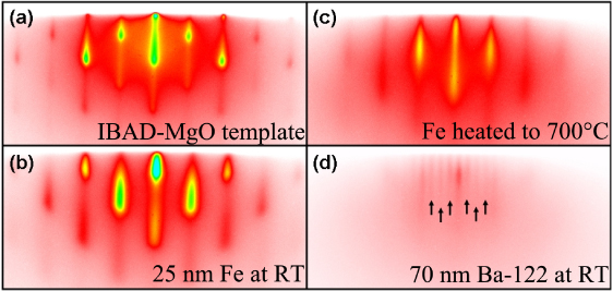
Figure 1. RHEED images of the film evolution: IBAD-MgO template (a), 25 nm Fe at room temperature (b) and heated up to deposition temperature (c), 70 nm Ba-122 after deposition (d). The latter reveals an indication for a surface reconstruction by the appearance of additional peaks, marked with arrows.
Download figure:
Standard imageIn order to prove the epitaxial relationship and texture quality of the stacked layers, θ/2θ scans using Co Kα radiation and pole figure measurements using Cu Kα radiation were performed. The θ/2θ scan of a Ba-122/Fe bilayer on IBAD-MgO is compared to the bare substrate and a similar bilayer on MgO-SC in figure 2. Besides the peaks arising from Hastelloy, Y2O3 and the MgO template, only (00l) peaks of the Ba-122/Fe bilayer occur, proving the c-axis orientation of the film. The texture relation known from former investigations on MgO single crystals [1] is confirmed by pole figures (figure 3) of the Ba-122 (103) peak, the Fe (110) peak and the MgO (220) peak, respectively. The Ba-122 layer reveals a remarkably small FWHM of ΔφBa−122 = 1.7°, which is only twice the value typical for films on MgO-SC. An essential parameter for this significant texture improvement was the use of a high-quality IBAD-MgO template (ΔφMgO = 2.4°). Compared to a previous study [6] we were able to reduce the FWHM by a factor of three at similar deposition conditions. Further texture improvement of covering layers with respect to the IBAD-MgO template is commonly observed in YBCO-coated conductors [3]. There are several reasons for this effect. Due to overgrowth of misoriented grains the IBAD-MgO texture quality enhances with thickness [10]. Therefore the texture at its surface is not exactly represented by XRD, which yields the integral texture of the whole layer volume. On the other hand the prevailing texture quality of the template surface affects the growth of a covering layer, which thus can have a reduced FWHM of Δφ with respect to the template.

Figure 2. θ/2θ scan of the Ba-122/Fe bilayer on IBAD-MgO (bottom) in comparison to the bare technical substrate (center) and a similar bilayer on MgO-SC (top).
Download figure:
Standard image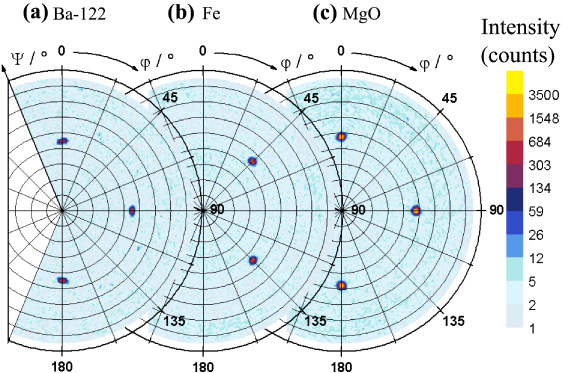
Figure 3. Pole figure measurements for (a) the Ba-122 (103) peak, (b) the Fe (110) peak and (c) the MgO (220) peak.
Download figure:
Standard imageIt is often observed that IBAD-MgO tends to grow slightly tilted with respect to the sample surface [10]. Utilizing an XRD four circle goniometer, an uncoupled ω-Φ scan was performed to determine the tilt of the MgO planes. The measurement geometry is displayed in the inset of figure 4 denoting all parameter definitions. To align the sample surface parallel to the xy-plane of the measurement geometry both angles ψ and ω were tilted while the sample was positioned covering half the beam at 2Θ = 0°. The rotation of the sample around the surface normal (Φ) at separate ω positions and 2Θ, which has been fixed for constructive interference of the MgO (002) planes, results in a projected precession of the MgO (002) normal around the z-axis. The amplitude of sin(Φ) equals the tilt of the MgO planes with respect to the substrate surface (figure 4), revealing 2.75° ± 0.25°.
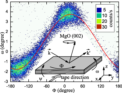
Figure 4. Two-axis scan of the (002) MgO peak in order to determine the orientation of the MgO planes with respect to the sample surface. The red line is a guide to the eye representing a sine function with an amplitude of 2.75°.
Download figure:
Standard imageIn order to correlate the microstructure and the superconducting properties of the sample, a TEM investigation was carried out. A lamella was prepared directly from the measured track using the in situ lift-out method [13]. The bright-field TEM overview shown in figure 5(a) confirms the formation of a closed Fe layer between the IBAD-MgO and the Ba-122 film. Islands, occasionally formed by the IBAD-MgO layer, are overgrown by Fe, leading to a sharp and smooth Ba-122/Fe interface (figure 5(b)). This emphasizes the necessity of a sufficient Fe buffer thickness to avoid the implementation of misoriented Ba-122 grains at facets of the MgO template. Defects extending throughout the whole Ba-122 film can be observed in the lamella in both crystallographic directions: the c-axis as well as the ab-axis (figures 5(c) and (d)). The former results from defects and grain boundaries in the MgO template which were transferred through the Fe buffer. The latter may be stacking faults. The size of these defects is not accurately determinable but exceeds the coherence length ξ ≈ 2 nm of Ba-122 [14].
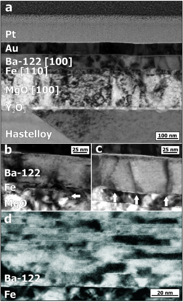
Figure 5. Bright-field TEM images. (a) Overview of the complete sample stack. (b) MgO step (see white arrow) is overgrown by the Fe buffer layer, resulting in a sharp interface between Fe and Ba-122. Defects (indicated by arrows) which penetrate throughout the whole Ba-122 film can be seen in the c-axis direction (c) as well as the a-axis direction (d).
Download figure:
Standard imageTransport measurements reveal a normal-state resistivity three orders of magnitude lower compared to films on MgO-SC, and an anomalous shape of the superconducting transition (figure 6(inset)). Next to the transition, a peak in the resistivity occurs followed by a sharp drop to zero. This behavior can be explained by a good conductivity between the Ba-122 film and the Hastelloy substrate. Physically, in the normal state, most of the current is shunted by the tape due to the small resistance barrier between film and tape caused by the minor MgO/Y2O3 buffer thickness. Therefore, between the voltage leads, only a low voltage drop is noticeable. Within the superconducting transition the current flowing through the Ba-122 increases with decreasing resistivity of the Ba-122, leading to an increased voltage drop. The measured resistance peaks and finally falls to zero when the film becomes fully superconducting on decreasing the temperature. This effect, caused by the architecture of the layer stack, can be described by a resistor network model [15]. Based on this model the resistivity of the Ba-122/Fe bilayer is reconstructed and compared to the transition of a similar film on MgO-SC in figure 6. The transition temperature, determined at 50% of the normal-state resistance, is 23 K for the film on IBAD-MgO and 26 K for the film on MgO-SC. Both a reduced preparation temperature while using metal substrates and additional doping of Ba-122 by transition metal ions may be responsible for the lower Tc value. Applying the resistor network, also the determined Jc can be corrected, however the error due to the conducting substrate for Jc exceeding 1 kA cm−2 is negligible [15].

Figure 6. Reconstructed transition using a resistor network model presented in [15] from transport measurement of the Ba-122 film on Fe/IBAD-MgO (inset) in comparison to a similar Ba-122 film on Fe/MgO-SC.
Download figure:
Standard imageFigure 7 shows the Jc(B) performance for temperatures of 4–18 K. The critical current density is monotonically decreasing with increasing magnetic field B parallel to the c-axis (dots) and perpendicular to it (lines). Jc values of more than 2 MA cm−2 are reached at low temperatures, similar to results reported by Katase et al [8]. The irreversibility field Hirr was determined by two methods: (i) the onset of the resistivity in R(T) curves (evaluated at Ec = 1 μV cm−1), and (ii) linear fits in Kramer plots (figure 8(a)) for Jc(B ∥ c). A slight curvature is visible in the plot for T = 10 K and T = 14 K, which is due to a small deviation in the Fp(H) parameters p, q from 0.5 and 2, respectively. The resulting Hirr can be fitted in the full temperature range using a power law Hirr ∼ (1−T/Tc)m with m = 1.6 ± 0.1 (figure 8(b)). Close to Tc, the determined Hirr is lower than the fit function due to the finite transition width (ΔTc ≈ 2 K), see inset in figure 8(b).
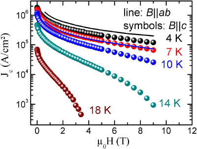
Figure 7. Magnetic-field-dependent critical current densities for H ∥ c. For temperatures 4 and 10 K a comparison to H ∥ ab (solid line) is given exemplarily.
Download figure:
Standard image
Figure 8. Kramer plots were fitted linearly ((a), solid lines) to determine Hirr (b). For temperatures near Tc, Hirr was additionally determined from the onset of the R(T) slopes ((b), open circles). The solid line represents a fit with Hirr ∼ (1−T/Tc)1.6 ((b), inset).
Download figure:
Standard imageAt all fields and temperatures we obtain the relation Jc(B ∥ c) < Jc(B ∥ ab). To get a deeper insight regarding the presence of c-axis correlated pinning, we performed angular dependent Jc measurements, where Θ is the angle between the applied magnetic field direction and the crystallographic c-axis. The angular dependent Jc(Θ) in maximum Lorentz force geometry and tape direction shows an asymmetry at low fields and temperatures, as illustrated for 10 K at 2–9 T in figure 9(a). In general, such an asymmetry might be caused by either a vicinal film structure or tilted correlated defects [17]. For thin films on IBAD templates, usually a vicinality is expected since the IBAD-MgO often grows up to 10° tilted with respect to the tape normal. Similar results were reported for YBCO thin films on IBAD-MgO and explained as a result of a vicinal film structure [18, 19].

Figure 9. Angular-dependent Jc (a) for different fields at 10 K. The crystallographic ab-planes were determined from the position of the ab-peak at high magnetic fields. The ab-peak position shifts to lower angles with decreasing magnetic field at 4 K (b). The solid line is a guide to the eyes. The inset shows the peak in Jc for the ab-direction. (c) The corresponding pinning force density for B ∥ c.
Download figure:
Standard imageThe crystallographic ab-planes were determined from the position of the ab-peak at high magnetic fields. In figure 9(b) the position of the ab-axis peak is illustrated in dependence of the applied magnetic field. For fields below μ0H0 ≈ 1 T we find an increasing shift of the peak regarding the ab-planes with decreasing field. With the upper critical field  in the order of 50 T, the corresponding reduced field
  is close to 0.02, which is in good agreement with values observed by Maiorov et al for YBCO-coated conductors and Silhanek et al [18, 20]. The sign of the shift corresponds to the 'anisotropy dominated case', described by Silhanek et al. This contradicts the expected 'geometry dominated case' for thin films. However, for a vicinal film the situation is more complicated and there is often no clear distinction possible because both effects may be present.
The position of the c-axis peak is not accurately traceable for fields above 3 T due to a decreasing height with increasing field. However, the angular-dependent Jc at 1 and 2 T reveal a similar peak position of Δθmax ≈ 3°. According to the XRD measurement described above, this direction is very close to the surface normal. On one hand, due to the large splay of c-axis oriented defects imaged with TEM, the position of this peak may be dominated by the geometry of the sample rather than the direction of the defects. On the other hand Maiorov et al reported a shift of the c-axis peak towards the substrate normal for high fields due to a different type of defects [18, 19]. For a small amount of inclined defects, this mechanism will dominate the pinning also for low fields, such as 1 and 2 T, resulting in a constant peak position parallel to the substrate normal in the traceable regime, as observed here. The identification of this effects is still the subject of further studies.
The pinning force density Fp for B ∥ c at different temperatures is displayed in figure 9(c). For 18 K, Fp can be fitted to Fp ∼ hp(1−h)q, where h = H/Hirr, with p = 0.5 and q = 2. This suggests shear breaking as the dominant depinning mechanism [16], where correlated pinning at columnar defects is less important. With decreasing temperature the maximum Fp shifts to lower h, and q increases due to a combination of random and extended defects in the influence of Fp. This is further evidenced by the c-axis peak vanishing with increasing field and temperature.
4. Conclusions
Using an Fe buffer on IBAD-MgO we demonstrated the optimization of important physical properties such as Tc and Jc by improving the texture quality of the Ba-122 film. Critical current densities comparable to films on MgO-SC are achieved. The conductance of the used buffer layer shunts the current and thus significantly influences the shape of the resistive transition. On the other hand a conducting buffer protects the superconducting layer if Jc is exceeded, since all current will be shunted by the metal tape. This is an important property for applications. However, the correction in Jc due to this influence is negligible for temperatures lower than 0.8 Tc. The angular-dependent Jc reveals minor correlated c-axis pinning due to a low defect density, the origin of which cannot clearly be attributed to inclined defects.
Acknowledgments
This work was partially supported by the DFG under grant no. HU1726/2 and by the European Commission under project SUPERIRON, grant no. 283204. The authors thank M Kühnel and U Besold for their technical support, A Kauffmann for helpful discussions and T Thersleff for scientific input into the TEM investigations.