
Abstract
The current transport mechanisms of Ag Schottky contacts to Zn-polar and O-polar bulk ZnO single crystals were investigated over the temperature range of 100–300 K. Using the thermionic emission (TE) model, Schottky contacts to Zn-polar face were found to have higher barrier heights (lower ideality factors) than those to O-polar face. Compared to the theoretical value of n-type ZnO, the higher Richardson constant was obtained for both polar faces in the modified Richardson plot, indicating that the TE model, which considers barrier inhomogeneity, cannot adequately explain the current transport. Temperature-dependent tunneling characteristics showed that the tunneling current was dominant for the Zn-polar face over the entire temperature range (100–300 K). For the O-polar face, the tunneling current was dominant mainly at low temperatures (100–200 K) and the TE component contributed strongly to the current transport above 200 K.
Export citation and abstract BibTeX RIS
1. Introduction
ZnO has attracted considerable interest as a semiconductor for optoelectronic applications, such as light-emitting diodes, ultraviolet (UV) detectors, white-light sources and solar cells, due to its wide band gap (3.4 eV at 300 K), high exciton binding energy (60 meV) and excellent radiation hardness [1–5]. ZnO crystallizes in the wurtzite structure, similarly to GaN; however, in contrast to GaN, ZnO is available as large bulk single crystals, which is an advantage of ZnO over GaN [6]. Currently three main techniques are used to grow bulk ZnO single crystals: hydrothermal, pressurized melt-grown and chemical vapor transport methods [7]. These three methods utilize different growth mechanisms, resulting in bulk ZnO crystals grown at different rates and subsequent dissimilar crystalline quality and intrinsic defect density. Metal-semiconductor (MS) contacts are the basic building blocks for device fabrication and can be used to investigate these defects. Additionally, an understanding of carrier transport across the MS contacts is required to achieve high-performance ZnO-based devices.
Previous research has shown that the barrier heights do not correlate with the metal work functions, suggesting that many factors, such as surface state, surface morphology and surface contamination, influence the electrical properties of the contacts [8, 9]. The existence of nonzero net dipole moments perpendicular to the Zn-polar (0 0 0 1) and O-polar (0 0 0  ) surfaces has been shown to lead to different interfacial structures in the Schottky contacts [10]. Silver oxide Schottky contacts on the Zn-polar surface have been shown to have higher barrier heights than those on the O-polar surface [11]. The responsivity of the Pt Schottky photodiode was observed to be two times higher on the Zn-polar surface than on the O-polar surface [12]. In contrast, Coppa et al reported no significant polarity effect in Au contacts to the Zn-polar and O-polar faces of single crystal ZnO wafers, which was attributed to the removal of hydrocarbon and hydroxide contamination [13]. A recent study demonstrated that different surface treatments are required in order to obtain good Schottky contacts to bulk ZnO grown by different methods [14]. However, there are few reports on the temperature-dependent current transport mechanism of Schottky contacts to bulk ZnO single crystals [15, 16]. In this paper, we describe the temperature-dependent electrical characteristics of Ag Schottky contacts to Zn-polar and O-polar bulk ZnO single crystals, considering barrier inhomogeneity.
2. Experimental details
An unintentionally doped, pressurized melt-grown, Zn-polar and O-polar bulk ZnO single crystal wafer purchased from Cermet Inc., was used in this investigation. The wafer was 5 × 5 × 0.5 mm3 with a single side polished by the manufacturer. The room-temperature carrier concentration assessed by Hall-effect measurements was ∼1 × 1017 cm−3. Before metallization, the sample was ultrasonically cleaned using organic solvents. Silver Schottky contacts (50 nm thick) were deposited by radio-frequency (RF) magnetron sputtering through a shadow mask onto the polished side of the samples. For ohmic contact, In metal was rubbed onto the entire back surface. Temperature-dependent current–voltage (I–V) measurements were performed on the several Schottky contacts for both polar faces with an HP 4156B semiconductor parameter analyzer and a cryogenic probe station (Janis ST-500).
3. Results and discussion
Figure 1 shows the semi-logarithmic I–V characteristics measured over a temperature range of 100–300 K for both polar faces. The current values for both the forward and reverse biases did not decrease monotonically with decreasing temperature. Similar results have been observed in Au/ZnO Schottky diodes [17]. Schmidt et al showed that bulk samples that were highly resistive in air could be reversibly transformed to a highly conducting state under vacuum, which was attributed to an electron conducting surface channel at the ZnO surface [18]. In other words, the conductive accumulation layer is compensated by acceptor-like adsorbates, such as O2 and H2O in ambient air, whereas the surface conductivity rises due to the removal of some O2 and H2O adsorbates from the surface under vacuum [15]. Therefore, it could be induced that surface compensation due to acceptor-like adsorbates occurred to varying extents at each temperature and this compensation effect might explain the abnormal temperature-dependent I–V behaviors as shown in figure 1.
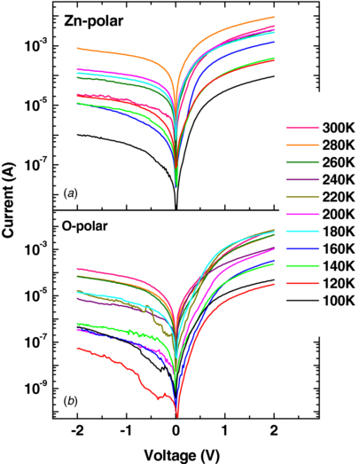
Figure 1. Semi-logarithmic I–V characteristics for the Ag Schottky contacts to (a) Zn-polar and (b) O-polar bulk ZnO over the temperature range of 100–300 K.
Download figure:
Standard imageThe forward bias characteristics of a Schottky diode based on the thermionic emission (TE) model are given by [19]


where I0 is the reverse bias saturation current, A is the device area, A** is the effective Richardson constant (32 A cm−2 K−2 for n-ZnO), ϕB is the effective Schottky barrier height, n is the ideality factor, V is the applied voltage and RS is the series resistance. For values of V greater than 3kBT/q, the ideality factor can be obtained from the slope of the linear region of the ln(I)–V curves under forward bias. The temperature dependence of the ideality factor and the barrier height determined from I–V measurements are shown in figure 2. For both polar faces, the barrier height (ideality factor) was found to increase (decrease) with increasing temperature. The lateral variation in the barrier heights has been used to explain such temperature dependence [20]. The current conduction at low temperatures was dominated by the patches of lower barrier height with a larger ideality factor. As the temperature increases, the dominant barrier height will increase because more electrons have sufficient energy to surmount the higher barrier. Figure 2 shows that the ideality factors at room temperature were much larger than unity, which has been attributed to the presence of interfacial states and an insulator layer between the metal and semiconductor [21].

Figure 2. (a) Effective barrier height and (b) ideality factor as a function of temperature. Lines in (b) represent the calculated ideality factors using equation (6).
Download figure:
Standard imageFurther examination showed that, for both polar faces, the ideality factor decreased rapidly with increasing temperature up to 200 K, while its variation was small above 200 K. Assuming a Gaussian distribution for the barrier heights over the Schottky contact area characterized by a zero-bias mean barrier height  and a standard deviation (σ0), which is a measure of the barrier homogeneity, the effective barrier height, (ϕB), gives the following expression:

where the temperature dependence of σ0 is usually negligible [21]. According to equation (3), the plot of ϕB versus 1/2kBT should be a straight line. As shown in figure 3, the plot can be well described by two straight lines, rather than a single line. Linear fits to the plot from the Zn-polar face yielded the values of  = 0.89 eV and σ0 = 0.145 V over the temperature range of 220–300 K (region 1) and the values of
  = 0.47 eV and σ0 = 0.071 V over the temperature range of 100–200 K (region 2). The linear fitting for the O-polar face yielded the values of
  = 0.72 eV and σ0 = 0.105 V over the temperature range of 220–300 K (region 1) and the values of
  = 0.54 eV and σ0 = 0.078 V over the temperature range of 100–200 K (region 2). These results may indicate the presence of a double Gaussian distribution of barrier heights, which was attributed to the nature of the inhomogeneities themselves [22]. In addition, the lower σ0 value for the O-polar face compared to the Zn-polar face in region 2 indicates a relatively uniform distribution of barrier heights over the contact area.
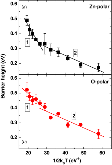
Figure 3. Effective barrier height (ϕB) versus 1/2kBT plot for the Ag Schottky contacts to (a) Zn-polar and (b) O-polar bulk ZnO with a double Gaussian distribution of barrier heights. The experimental data show linear variation in the two temperature regions with a transition around 200 K.
Download figure:
Standard imageConsidering the barrier inhomogeneity, the modified Richardson plot can be obtained from equations (2) and (3):

Figure 4 shows the ln(I0/T2) − q2σ20/2k2BT2 versus 1000/T plots for the regions 1 and 2. The linear fitting for the Zn-polar (O-polar) faces yielded a zero-bias mean barrier height of 0.90 (0.73) and 0.48 (0.55) eV over the temperature ranges of 220–300 K and 100–200 K, respectively. The intercepts at the ordinate for the Zn-polar (O-polar) face produced an effective Richardson constant of 49.0 (46.3) A cm−2 K−2 (in region 1: 220–300 K) and 75.3 (49.7) A cm−2 K−2 (in region 2: 100–200 K). The mean barrier heights were very similar to those obtained from the ϕB versus 1/2kBT plot shown in figure 3. However, the obtained Richardson constants were larger than the theoretical value of 32 A cm−2 K−2 for n-type ZnO. This discrepancy implies that the TE model cannot adequately explain the current transport in the Ag Schottky contacts to both polar faces.
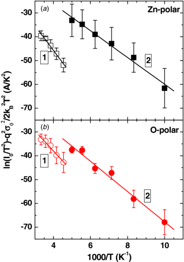
Figure 4. Modified Richardson plot of ln(I0/T2)–q2σ2/2kB2T2 versus 1000/T for the Ag Schottky contacts to (a) Zn-polar and (b) O-polar bulk ZnO according to a double Gaussian distribution of barrier heights. The straight lines 1 and 2 indicate the linear fits to the experimental data over temperature ranges of 220–300 K and 100–200 K, respectively.
Download figure:
Standard imageWhen the thermionic field emission (TFE) or field emission (FE) models are used to describe the current transport, the forward bias currents are given by [23]

with

where E00 = qh/4π(ND/m*ε)1/2 is the characteristic energy related to the tunneling probability. The current transport mechanism is dependent on the tunneling parameters E00: TE for E00/kBT ≪ 1, TFE for E00/kBT ∼ 1 and FE for E00/kBT ≫ 1 [23]. Figure 5 shows the values of nkBT as a function of kBT. For the Zn-polar face, nkBT (=E0) values are more or less constant over the measured temperature range. When FE dominates, the E0 will lie on a straight line and is independent of temperature, which is very close to the E00 values [24]. This indicates that the tunneling current dominated for the Zn-polar face over the entire temperature range. The average E0 value was 88.2 meV, close to the E00 value of 85.4 meV obtained from the fitting of equation (6) to ideality factors (solid line in figure 2(b)). For the O-polar face, a straight line with a slope of 2.9 was obtained using the TE model and matched to the experimental data well over the temperature range of 220–300 K. The large deviation of the ideality factor from unity arises from interfacial effects, as described before. However, over the temperature range of 100–200 K, the experimental data were far off the straight line fitted at high temperatures, and do not show a clear temperature dependence, indicating the contribution of the tunneling current. Similar to the Zn-polar face, the average E0 value was found to be 63.8 meV over the temperature of 100–200 K, close to the E00 value of 61.2 meV obtained from the fitting to n values (dashed line in figure 2(b)).
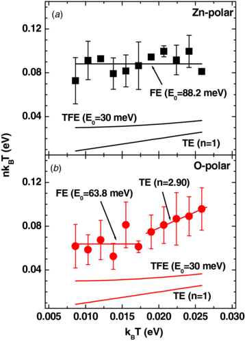
Figure 5. Plot of experimental and theoretical nkBT values as a function of kBT for the Ag Schottky contacts to (a) Zn-polar and (b) O-polar bulk ZnO.
Download figure:
Standard imageFigure 6 shows the ln(I) versus V plots at small forward biases for the different temperatures. Above 200 K, the ln(I)–V curves intersect to each other for both polar faces at some point, which may be due to the series resistance, interfacial layer near the interface and interfacial states [25, 26]. The slope of the ln(I)–V curves is almost the same and parallel for the Zn-polar face, indicating again that the tunneling current was dominant over the entire temperature range. In contrast, the slope for the O-polar face decreased above 200 K, indicating the contribution of the TE component.
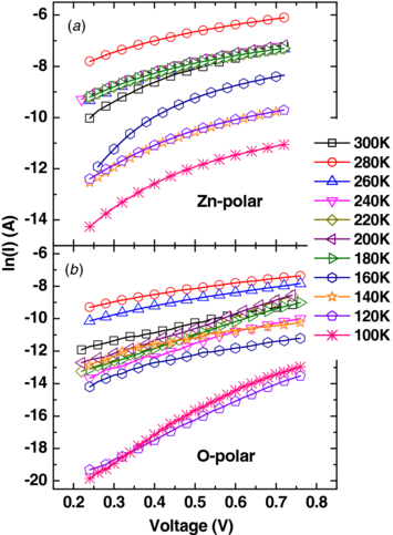
Figure 6. ln(I) versus V plots at small forward biases for the Ag Schottky contacts to (a) Zn-polar and (b) O-polar bulk ZnO over the temperature of 100–300 K.
Download figure:
Standard imageThe TFE or FE model was used to analyze the forward I–V characteristics in more detail using equation (5) and the saturation current densities given by [27]
where ξ = kBT/qln(NC/ND) is the energy difference between EC and EF, NC is the effective density of states in the conduction band, and ND is the carrier concentration. The obtained barrier heights are tabulated in table 1. The fundamental or flat-band barrier height was also calculated using the ideality factor (n) and the effective barrier height (ϕB), given by the TE model [28]:

Table 1. Summary of calculated barrier heights.
| TFE model ϕB (eV) | Flat-band ϕB (eV) | FE model ϕB (eV) | |||
|---|---|---|---|---|---|
| Temp. (K) | Zn-face | O-face | Zn-face | O-face | Zn-face |
| 100 | 1.12 (± 0.14) | 1.37 (± 0.23) | 1.78 (± 0.37) | 1.45 (± 0.30) | 1.52 (± 0.27) |
| 120 | 1.27 (± 0.17) | 1.46 (± 0.31) | 1.72 (± 0.22) | 1.50 (± 0.34) | 1.84 (± 0.31) |
| 140 | 1.46 (± 0.16) | 1.42 (± 0.40) | 1.61 (± 0.14) | 1.46 (± 0.44) | 1.92 (± 0.16) |
| 160 | 1.34 (± 0.19) | 1.36 (± 0.34) | 1.58 (± 0.22) | 1.27 (± 0.29) | 1.66 (± 0.30) |
| 180 | 1.27 (± 0.02) | 1.51 (± 0.29) | 1.02 (± 0.22) | 1.55 (± 0.34) | 1.54 (± 0.04) |
| 200 | 1.36 (± 0.08) | 1.32 (± 0.16) | 0.96 (± 0.32) | 1.31 (± 0.18) | 1.68 (± 0.14) |
| 220 | 1.38 (± 0.09) | 1.54 (± 0.23) | 1.42 (± 0.06) | 1.50 (± 0.23) | – |
| 240 | 1.46 (± 0.10) | 1.58 (± 0.23) | 1.54 (± 0.03) | 1.57 (± 0.25) | – |
| 260 | 1.41 (± 0.06) | 1.52 (± 0.38) | 1.22 (± 0.17) | 1.49 (± 0.40) | – |
| 280 | 1.45 (± 0.04) | 1.51 (± 0.38) | 1.19 (± 0.19) | 1.46 (± 0.38) | – |
| 300 | 1.35 (± 0.12) | 1.63 (± 0.19) | 1.36 (± 0.10) | 1.57 (± 0.18) | – |
Unlike the zero-bias barrier height, the electric field in the semiconductor is zero under the flat-band condition. Thus, the effects of tunneling and image force lowering on the I–V characteristics are negligible. For the O-polar face, the calculated flat-band barrier heights were very similar to those from the TFE model for all measurement temperatures, indicating that the TFE model can adequately explain the current transport. For the Zn-polar face, the flat-band barrier heights were similar to those from the TFE model above 200 K, indicating that the current transport is governed by the TFE model. However, a large discrepancy was observed below 200 K. For this temperature range, the FE model was applied to the forward I–V characteristics. Compared to those from the TFE model, the FE model produced values closer to the flat-band barrier heights, although the difference between the FE and flat-band values is still large. Thus, the FE model is more appropriate than the TFE model at lower temperature. Both the flat-band barrier heights and those from the TFE model show that the O-polar face revealed higher barrier heights than the Zn-polar face.
It has been reported that both the Zn-polar and O-polar faces react in ambient with water to form a hydroxide (OH) accumulation layer on the ZnO surface, increasing the surface conductivity [15, 29]. The surface sheet carrier concentration was found to increase with increasing intensity of the OH peak in the x-ray photoemission spectroscopy (XPS) spectrum [30]. Metal diodes on as-received Zn-polar and O-polar faces were shown to be ohmic due to the surface adsorbates, such as C and OH, on both polar faces [31]. After hydrogen peroxide (H2O2) treatment, Gu et al observed that the C impurity on the ZnO surface could not be removed effectively and the resultant rectifying characteristics of the Au/ZnO Schottky contacts were attributed to the removal of OH rather than the C impurity [32]. Because no acid or plasma treatment was carried out before Schottky metallization in our work, it can be inferred that the conductive OH accumulation layer formed on both polar faces and degraded the rectifying characteristics. We observed the highly ohmic behavior in the Pt Schottky contacts to ZnO for both polar faces. However, unlike Pt Schottky contacts, Ag Schottky contacts to both polar faces showed some degree of rectifying behavior. Silver oxide Schottky contacts to bulk ZnO grown by both the hydrothermal and pressurized melt-grown methods have been reported to be highly rectifying [11]. A higher degree of oxidation of the Ag/ZnO contacts was shown to improve the rectifying characteristics [33]. Using Poisson-modified Thomas Fermi approximation (MTFA) calculations, Allen et al showed that the near-surface band bending was stronger and the corresponding surface sheet carrier density was higher in the Zn-polar face compared to the O-polar face [34]. Furthermore, based on the first-principle studies, Dong and Brillson found that Schottky barriers were strongly dependent on the interfacial chemical bonding and suggested that noble metal-oxygen bonds (e.g., Au-O or Ag-O) can form Schottky contacts, while metal-Zn bonds are associated with ohmic-like behavior [35]. Since the barrier heights of the O-polar face are higher than those of the Zn-polar face, it is likely that a higher degree of oxidation occurred for the O-polar face.
It has been shown that the bulk carrier concentration of pressurized melt-grown ZnO is mainly due to shallow donors at ∼50 meV below the conduction band [36] and the bulk carriers do not decrease significantly with decreasing temperature down to 100 K, unlike hydrothermally grown ZnO. The bulk carrier concentration for the samples used in this work was about 1017 cm−3, which corresponds to about 4 meV for the E00 value, much lower than the values as presented in figure 5. Based on these results, we propose the following current transport for both polar faces. For the Zn-polar face, the conductive surface layer mainly contributes to the current transport by tunneling over the entire temperature range (100–300 K). For the O-polar face, the current flow is mainly controlled by the tunneling component over the temperature ranges of 100–200 K due to the conductive surface layer. However, the level of current flow is relatively low compared to the Zn-polar face, due to the higher degree of oxidation, which reduces interfacial defects [37]. Above 200 K, the bulk carriers have sufficient energy to surmount the barrier. Thus, the current transport is strongly associated with the TE component.
4. Conclusion
We investigated the temperature-dependent current transport mechanisms of Ag Schottky contacts to Zn-polar and O-polar bulk ZnO single crystals. It was observed that the barrier heights varied, with a double Gaussian distribution for both polar faces: one for a high-temperature region (220–300 K) and the other for a low-temperature region (100–200 K). However, compared to the theoretical value of n-type ZnO, the Richardson constant from the modified Richardson plot was higher for both polar faces, indicating that the TE model with barrier inhomogeneity cannot adequately explain the current transport. Analyses of the ln(I)–V curves and the nkBT (E0) values at different temperatures showed that the tunneling current was dominant for the Zn-polar face over the entire temperature range (100–300 K). For the O-polar face, the tunneling current was dominant below 200 K and the TE component contributed to the current transport above 200 K but maintained a high level of tunneling current.
Acknowledgments
This work was supported by the Basic Science Research Program (2010-0003594) through the National Research Foundation of Korea funded by the Ministry of Education, Science and Technology (MEST) and by the MEST & Daegu Gyeongbuk Institute of Science and Technology (DGIST) (10-BD-0101, Convergence Technology with New Renewable Energy and Intelligent Robot).