

Abstract
Understanding the mechanism of resistive switching in a memory device is fundamental in order to improve device performance. The mechanism of current switching in a basic organic write-once read-many (WORM) memory device is investigated by determining the energy level alignments of indium tin oxide (ITO), poly(9-vinylcarbazole) (PVK) and aluminum (Al) using x-ray and ultraviolet photoelectron spectroscopy, current–voltage characterization and Auger depth profiling. The current switching mechanism was determined to be controlled by the interface between the ITO and the PVK. The electric field applied across the device causes the ITO from the uneven surface of the anode to form metallic filaments through the PVK, causing a shorting effect within the device leading to increased conduction. This was found to be independent of the PVK thickness, although the switch-on voltage was non-linearly dependent on the thickness. The formation of these filaments also caused the destruction of the interfacial dipole at the PVK–Al interface.
Export citation and abstract BibTeX RIS
1. Introduction
The recent developments in organic and polymer devices have seen a rise in the number of polymer and organic materials under investigation, especially with regards to the energy levels of these materials. Poly(9-vinylcarbazole) (PVK) is one of the most common and versatile organic semiconductors, with a deep highest occupied molecular orbital (HOMO) and high triplet energy [1]. It can be used as a component of non-volatile, write-once read-many (WORM) memory. Organic memory devices are a low-cost, ultrathin alternative to conventional, bulky optical and magnetic storage devices and when stacked can be used in three dimensions to achieve a vast storage capacity [2–4].
Many different organic materials have been used in the construction of these memory devices with the aim to improve the on–off current ratio and the retention stability, two key properties of memory devices [3, 5, 6]. These include polymer, graphene and carbon nanotube composites with PVK [7–10], the insertion of gold, titanium dioxide and hybrid nanoparticles [11–14], carbazole spacer polymers [15–17] and graphene electrodes [18, 19].
A wide range of mechanisms are used to account for the switching transition. Trapping, filamentary conduction, field-induced transfer and electrochemical doping are often used to explain the resistive switching [4]. However, few measurements go beyond the observation of resistive switching to address the issues necessary to distinguish between possible candidate mechanisms. In many organic-based devices, charge injection into conjugated materials is governed to a large extent by the interfaces and band-bending within the device [20]. Whether such effects are an important parameter that governs the resistive switching mechanism still remains a subject of debate. One notable example is the disappearance of the diffraction peaks at the copper(II) phthalocyanine (CuPc)–hexadecafluoro-copper-phthalocyanine (F16CuPc) interface after the conductivity transition [6]. The disappearance of the diffraction peaks are attributed to the destruction of the interfacial dipole. Such diffraction patterns originate from the ordered self-assembly layer due to the formation of an interfacial dipole layer [21]. Hence, it appears that the interfacial dipole might play an important role in controlling the injection of charges.
However, there has been no report of the energy levels and interfacial states being measured and mapped within these WORM devices in either the 'on' or 'off' states. Mapping the interfacial states will provide direct evidence of the role of the interfacial dipole in resistive switching. Furthermore, interfacial dipoles and band-bending are present in virtually all organic semiconducting–metallic interfaces. Direct evidence of the role of these effects in resistive switching is critical to understanding the wide range of mechanisms being proposed. In order to distinguish various possible mechanisms of resistive switching, pristine PVK without any doping is used. PVK is chosen as a WORM memory material as it has been proposed that the switching mechanism might be due to the destruction of the interfacial dipole [22]. Therefore, in this letter we use x-ray and ultraviolet photoelectron spectroscopy (XPS and UPS) to measure the energy levels of a WORM memory device consisting of ITO, PVK and Al in both the 'on' and 'off' states in order to determine the current switching mechanism. We also use Auger depth profiling in order to measure the elemental composition of the device as a function of the depth of an ITO–PVK–Al device to ascertain if there is any interfacial mixing of the electrodes and polymer.
2. Materials and methods
All materials were purchased and used as received without further purification. Poly(N-vinylcarbazole) (PVK) (average Mw = 25 000–50 000) were purchased from Sigma-Aldrich. Pre-patterned indium tin oxide (ITO) with sheet resistance 25 Ω/□ was cleaned sequentially using deionized water, acetone, isopropyl alcohol and deionized water again followed by oxygen plasma treatment for 5 min. For the device fabrication, 8 wt% PVK dissolved in chlorobenzene was spin coated onto ITO at various speeds to produce PVK thicknesses of 50 nm, 100 nm, 240 nm and 400 nm. Then the substrates were baked at 100 °C for 10 min. A separate device was made whereby 100 nm of poly(3,4-ethylenedioxythiophene) polystyrene sulfonate (PEDOT:PSS) was spin-coated onto the ITO, baked at 100 °C for 10 min and then 100 nm of PVK spin-coated on top. Finally, the device cathode, which consists of 100 nm Al, was vacuum deposited at a base pressure of 2.5 × 10⁻⁶ mbar. These devices were encapsulated using UV curable epoxy and a glass lid. The current (I)–voltage (V) characteristics were measured using a Keithley 2612B SourceMeter by scanning the voltage from 0 V to 6 V and then back to 0 V. The aluminum is always at a lower potential than the ITO during the scanning. The devices used for XPS and UPS analysis had vacuum deposited Al of thicknesses 1 nm, 3 nm, 5 nm, 7 nm and 9 nm. The elemental composition depth profiling was further studied using a JEOL JAMP-9500F field emission Auger microprobe. An argon ion beam was used as a beam source and the etch-rate used for the depth profiling measurement was 13.6 nm min−1.
3. Results and discussion
The current–voltage characteristics from the first voltage sweep of the WORM devices with varying polymer thicknesses of 50 nm, 100 nm, 175 nm and 400 nm are shown in figure 1(a). As the applied voltage is increased for the first time, the current increases by at least one to two orders of magnitude at around 2–3 V; such a transition corresponds to the writing process of a digital memory cell, as shown in figure 1(a). The current reaches the source-meter current compliance level of 0.2 mA cm−2, whereby it appears to saturate. However, this is not true space-charge limited current (SCLC) saturation within the PVK layer, but only the source-meter safety level. This is to prevent burning of the devices. The current remains constant until the applied voltage is significantly lowered and the current also decreases to zero. Not shown here is the fact that when the applied voltage is increased for a second time the current increases to its 'on' state value, and this is then repeated many times with the same results over a period of 2–4 min, confirming the WORM statuses of these devices. This happens for all thicknesses of PVK, Figure 1(b) shows the switch-on voltage and corresponding electric field of each of these devices, and it is quite clear that, although the resistive memory is itself independent of PVK thickness, the switch-on voltage at which this occurs is dependent. There is a strong non-linear dependency with PVK thickness, which suggests that a 'shorting' effect between the ITO and Al interfaces is the cause of the resistive switching.

Figure 1. (a) Current–voltage characteristics of ITO–PVK–Al memory device during first sweep for different PVK thicknesses. The switched-on voltages are determined by intersections of the asymptotes of rapid increase of current and the 'off' state current. (b) Switch-on voltage and electric field as a function of PVK thickness for each of the ITO–PVK–Al devices.
Download figure:
Standard image High-resolution imageThis is further corroborated when a 60 nm layer of PEDOT:PSS is inserted between the ITO electrode and the 100 nm PVK polymer layer. The PEDOT:PSS layer acts as a hole injector in many organic light emitting diodes, and it has also been found to have resistive switching qualities via reduction and oxidation [23, 24]. However, in our case, it provides an extra interface within the WORM device to help prevent a direct shorting between the anode and cathode. The I–V characteristics seen in figure 2 show that resistive switching is completely absent and that the device remains in a constant 'off' state as opposed to the I–V characteristics of the ITO–PVK–Al WORM memory device, also shown in figure 2, which confirm that the device remains in the 'on' state after initial switching and has stability over long periods of time.
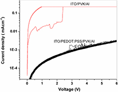
Figure 2. Current–voltage characteristics of an ITO–PVK–Al and an ITO–PEDOT:PSS–PVK–Al device running over several tens of cycles with a PVK thickness of 175 nm.
Download figure:
Standard image High-resolution imageIn order to explain this phenomenon the ITO–PVK and PVK–Al interfaces of the devices were examined using XPS and UPS, where the Al layer had varying thicknesses of 1 nm, 3 nm, 5 nm, 7 nm and 9 nm.
The band diagram of the ITO–PVK–Al device before it is subjected to a potential difference between the anode and cathode is shown in figure 3 along with the UP spectra used to calculate the work function and HOMO levels for the PVK–Al interface. There is a 0.35 eV vacuum level dipole between the ITO and PVK and the same difference between the Fermi level and the HOMO of the PVK. However, there is some band-bending at the interface of these two materials, which decreases the energy barrier of the holes at the interface to 0.25 eV. The vacuum level dipole at the PVK–Al interface (also referred as interfacial dipole) is much larger at 0.85 eV and the difference between the PVK HOMO and the Al Fermi level is similar at 0.80 eV. The band-bending of the PVK HOMO at the interface shifts to lower binding energies, moving 0.35 eV towards the Fermi level, whilst the band-bending in the Al shifts to higher binding energies by 0.45 eV towards the HOMO level. The nitrogen atom on the carbazole unit carries a lone pair of electrons and provides an electron donating ability to the carbazole moiety. This results in electron transfer between the molecule and the aluminum. Such interactions of the nitrogen lone pairs with the aluminum surface have been observed recently [25]. The carbazole molecule is also a well known chromosphere of practical relevance, having a fairly large static dipole moment of 2 D [26]. The combined interaction of the lone pair of electrons with the aluminum and the presence of permanent dipole moments might contribute to the interfacial dipole.
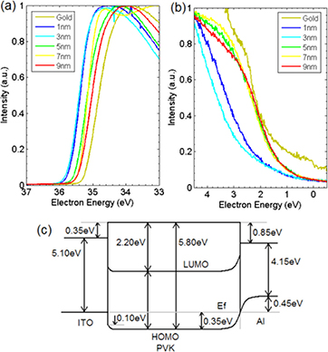
Figure 3. Ultraviolet photoelectron spectra of the PVK–Al interface before charging with varying Al film thickness. (a) High-energy and (b) low-energy cut-off point representing the work function and HOMO levels respectively. (c) Full band diagram of the ITO–PVK and PVK–Al interfaces when the WORM memory device is in the 'off' state as measured by UPS and XPS.
Download figure:
Standard image High-resolution image10 V was then applied across the device in order to change it into its 'on' state, and the band diagram of the device is shown in figure 4 along with the UP spectra of the PVK–Al interface. The ITO–PVK interface remains the same in figure 4, as we cannot observe the changes at the ITO–PVK interface in a complete ITO–PVK–Al device as the electron escape depth in most materials is at maximum 10 nm; however, the PVK–Al interface changes dramatically. The surface dipole has disappeared and the Fermi level of the Al has been shifted so that the energy gap to the HOMO level of the PVK is now 1.65 eV. This results in vacuum level alignment at the PVK–Al interface. However, it is unclear at this point whether the changes seen in the PVK–Al interface are the cause of the resistive switching or come about because of the switching.
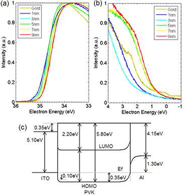
Figure 4. Ultraviolet photoelectron spectra of the PVK–Al interface after charging with varying Al film thicknesses. (a) High-energy and (b) low-energy cut-off point representing the work function and HOMO levels respectively. (c) Full band diagram of the ITO–PVK and PVK–Al interfaces when the WORM memory device is in the 'on' state as measured by UPS and XPS. The vacuum level is now aligned at the PVK–Al interface.
Download figure:
Standard image High-resolution imageThe strong interactions between the Al and the lone-pair electrons on the nitrogen atom of the carbazole have created an interfacial dipole. The formation of the dipole at the aluminum surface results from the orientation of lone pairs of electrons from PVK to the aluminum as illustrated in figure 5. The adsorption of lone pairs of electrons polarizes the aluminum surface and the surface becomes more electropositive. This results in the dipole moment pointing towards the aluminum. We speculate that the reorientation of molecules can form well ordered layers within the PVK. Such behavior has been recently observed in a poly [(9,9-bis(3'-(N,N-dimethylamino)propyl)-2,7-fluorene)-alt-2,7-(9,9–dioctylfluorene)]–ITO system [26]. The length of these dipoles is usually sub-monolayer to a monolayer at most, which in PVK is about 0.4 nm [27, 28]. This means the PVK–Al dipole length is smaller than the PVK band-bending at the interface, which is calculated at about 2 nm using the method described in [29].

Figure 5. Diagram and schematic of the orientation of the dipole across the PVK–Al interface.
Download figure:
Standard image High-resolution imageOne way in which we can observe changes at the ITO–PVK interface in a complete ITO–PVK–Al device before and after switching is by using Auger depth profiling. An ITO–PVK–Al device was created for the purpose using 400 nm PVK and 100 nm Al. Figure 6 shows the Auger depth profile of aluminum, carbon, indium, tin and oxygen in plots (a)–(d) respectively. The Al profile decreases at 100 nm as expected although there is significant penetration into the PVK as expected both before and after switching, which suggests that the deposition of hot Al onto a polymer such as PVK will result in some initial Al penetration that has nothing to do with the device being charged. This could be the cause of the initial vacuum level dipole at the PVK–Al interface and subsequently the 0.80 eV band-bending that was also observed. This is a common phenomenon when hot metal is vacuum-deposited onto a polymer and has been observed before [30]. However, there is no change to this penetration after charging, which indicates that there is no additional Al penetration after resistive switching and the change seen at the PVK–Al interface is not associated with this effect. The C profile shows the position of the PVK within the device, and although there is no PVK penetration into the Al there does appear to be some penetration on the other side into the PVK. Additionally, there is a reduction in carbon seen towards the ITO–PVK interface after the device has been charged but there is no change in the carbon content within the ITO itself. This suggests that the cause of the resistive switching occurs at the ITO–PVK interface but is not due to the PVK penetration of the ITO. Finally, looking at the In, Sn and O content in figures 6(b)–(d), it is clear to see that the elements within the ITO have penetrated very deep into the PVK – almost reaching the PVK–Al interface – after the device has been switched to its 'on' state. This is consistent with the metal filament effect seen in other memory devices [31, 32]. The spike of oxygen at the aluminum interface is the result of oxidation of the aluminum, probably during its initial vacuum-deposition. However, it is clear from figure 6(c) that there is no change in the oxygen level after the 'on' state has formed and thus it is not responsible for the resistive switching.

Figure 6. Auger depth profiling of a ITO–PVK (400 nm)/Al (100 nm) device showing the (a) aluminum and carbon, (b) indium, (c) oxygen and (d) tin content of the device as a function of depth.
Download figure:
Standard image High-resolution image
The elemental composition of these filaments is clear from figures 6(b)–(d) as it shows an increase in all three elements, indium, tin and oxygen, across the width of the PVK. By calculating the integrated count of each element before and after switching within the bulk of the PVK between 150 nm and 450 nm as seen in figure 6, we can determine the percentage increase of each of the elements in the PVK after the device is switched on. The indium appears to increase by 214%, whilst the number of tin atoms increases by 138% and finally the oxygen increases by a smaller margin of 61%. It is clear that there is an increase of all components of ITO across the PVK, but the filaments seem to be made up primarily of indium and tin atoms, with the former dominant in the filament composition.
The surface of ITO is naturally uneven and its work function is highly dependent on both its physical and chemical properties [33]. As such when the PVK is deposited onto the ITO the uneven surface causes many small physical displacements at the interface, which can provide inroads between the PVK polymer strands [34]. When a voltage is applied across the device, ITO is stripped from these displacements and is pulled into and across the PVK, where it combines to form filaments as seen in the Auger profiling depth of figures 6(b)–(d). These filaments essentially cause a 'shorting' effect for current across the PVK between the ITO and Al electrodes and this causes the vacuum level dipole at the PVK–Al interface to disappear. This is further corroborated by the fact that the extra PEDOT:PSS layer inserted between the ITO and PVK would prevent the filaments from reaching the PVK layer by means of the highly disordered, grain-boundary-like effect that the PEDOT:PSS/PVK interface would provide. Thus there is no evidence of resistive switching in the ITO–PEDOT:PSS–PVK–Al device [35]. Exactly how this causes the interfacial dipole to disappear is not yet clear, as the existence of a vacuum level dipole is based on both the physical and chemical attributes of the interface [36]. However, one can speculate that, since a direct path has been forged between anode and cathode, the easy replenishment of holes at the PVK side of the interface quickly negates the pre-existing electropositivity of the Al surface (interfacial dipole), and along with the disordering of the PVK molecules at the interface by the ITO filaments the PVK–Al vacuum level dipole is destroyed.
4. Conclusions
In conclusion, we have determined the mechanism that induces resistive switching in a simple ITO–PVK–Al WORM memory device using current–voltage characterization, UPS, XPS and Auger depth profiling. The reason for the resistance switching is the extension of ITO from the uneven anode surface into the PVK causing a shorting of the organic semiconductor and an easier route for holes to travel from the ITO anode to the Al cathode. This was confirmed when we inserted a 200 nm layer of PEDOT:PSS in between the ITO and PVK and found that no resistance switching occurs. Although we found that the presence of resistive switching is completely independent of the thickness of the PVK used, we did find that the switch-on voltage is non-linearly dependent on the PVK thickness. We have also found that, although the cause of the resistive switching occurs at the ITO–PVK interface, the effect that the switching has on the PVK–Al interface is substantial and results in the destruction of the interfacial dipole that is present at the interface before charging of the device occurs.
Acknowledgments
This research was supported by a University of Malaya Flagship project (FL017/2011), a University of Malaya Chancellery High Impact Research Grant (UM.C/625/1/HIR/195) and an MOHE Fundamental Research Grant (FP005-2013A). Special thanks to Surachet Rattanasuporn and Watcharapon Jenpiyapong at the Synchrotron Light Research Institute for their help in the photoelectron measurements.