

Abstract
Magnetic tunnelling junctions increasingly enter the market for magnetic sensor applications. Thus, technological parameters such as the lifetime characteristics become more and more important. Here, an analysis of the lifetime characteristics of magnetic tunnelling junctions using the Weibull statistical distribution for CoFeB/MgO/CoFeB junctions is presented. The Weibull distribution is governed by two parameters, the characteristic lifetime η of the population and the shape parameter β, which gives information about the presence of an infant mortality. The suitability of the Weibull distribution is demonstrated for the description of dielectric breakdown processes in MgO-based tunnelling junctions at different voltages. A study of the dependence of the characteristic lifetime extrapolated to the low voltage regime, and the β parameter on the nominal barrier thickness and the resistance × area product of the MgO barrier is shown. The influence of the RF deposition power for the MgO barrier and an annealing step on the Weibull parameters is also discussed.
Export citation and abstract BibTeX RIS
The use of magnetic tunnelling junctions (MTJs) in hard disc read heads is already widespread. As magnetic field sensors they are entering the field of industrial applications in the automotive branch, in robotics, and in machine automation in general. The major advantage of MTJ based sensors is their much higher sensitivity due to larger magnetoresistance values compared to conventional AMR and GMR technologies (anisotropic and giant magnetoresistance, respectively). Technologically, the larger signal amplitude can eliminate the need of a signal preamplifier with the subsequent simplification of the system design. Additionally, their typically larger resistance values make them promising candidates for green energy applications with low-consumption requirements, due to the reduction of the current needed to obtain a voltage signal. Consequently, the main sensor producers are developing new prototypes and products based on MTJs [1, 2].
In spite of the clear advantages, the use of MTJs in sensorics aside of read heads applications is still low, and AMR persists at the moment as the dominating technology. One of the main criticism points that prevents a faster adoption of the MTJ technology for sensors is their long-time stability against failure. The thin insulating layer responsible for the tunnelling effect is the weakest point. During working conditions the voltage drops over the few nanometer thick tunnelling barrier resulting in a large electrical field (107 V m−1). This field represents a strong stress agent being able, after a certain time, to produce a dielectric breakdown of the barrier and a device failure. This process is independent on electrostatic discharge (ESD) events which can also destroy the barrier. While the latter can be prevented with diverting on-chip circuits or by training of the mounting employees, the former cannot be avoided since the stress agent is present any time that the sensor/device is in use.
For a given junction, the time to a breakdown event cannot be predicted since we are handling here a stochastic process analog to metal failure under mechanical stress. The time to breakdown is a statistically distributed parameter. However, the failure rate for a given sensor population and its time evolution characteristics can be measured and analyzed using statistical methods. Here a report on a systematic study of the barrier thickness influence on the lifetime characteristics for CoFeB/MgO/CoFeB tunnelling junctions is presented. The effect of annealing and of the RF power during the MgO barrier deposition is also studied.
For the analysis of the lifetime characteristics, the Weibull distribution is used. This approach can be used in studies of failure events caused by a single stress agent (in our case the electrical field). The distribution does not take into account thermal or current-induced electromigration effects for which other statistical models are more appropriate. For this reason, the current density must be kept low which may complicate measurements for MTJs with very low resistance × area (RA) values. The suitability of the Weibull distribution for the description of breakdown processes in thin oxide layers [3] and, more concretely, for tunnelling devices has been already proven for MTJs with Al2O3 [4, 5] and MgO [6] barriers.
The Weibull probability density function f(t) describes the fraction of broken elements per time unit: [7, 8]
Here, η is the characteristic lifetime of the junction population and β is the shape parameter. For measurements, it is more convenient to use the Weibull cumulative function, which describes the total fraction F of broken elements after a certain time t:
It is evident that for  , 63.2% of the elements are broken. To understand the impact of the shape parameter β in the time evolution of the fraction of failed elements, figure 1 demonstrates three characteristic cases:
 Failure rate decreases with time. The population shows a large infant mortality, i.e. a significant fraction of the elements breaks shortly after the application of the stress agent (black line in figure 1). In general, this regime is not suitable for applications since a large part of an hypothetical sensor production will fail in an early stage.
- Failure rate increases with time. The behaviour is dominated by aging (dotted data and gray line). In addition, a time window exists for which the failure rate is negligible. This is the desired situation for applications since it allows the introduction of a guarantee time.
- Constant failure rate (dashed red line). This represents the transition between the two previous cases but it must be handled with care since it may point to an external random agent dominating the behaviour when this is always the case (e.g. a defective measurement setup generating peak voltages). The dependence of the lifetime η on the stress agent strength allows to distinguish between both situations.


Figure 1. Weibull cumulative function F(t), describing the total fraction of broken elements after a time t, calculated for different values of the shape parameter β. The time is given in units of the characteristic lifetime η.
Download figure:
Standard image High-resolution imageThe characterization of the breakdown processes was carried out for circular CoFeB/MgO/CoFeB junctions with a diameter of 10 μm. The barrier is deposited by RF-sputtering and a synthetic antiferromagnet layer structure is used. SiO2 wafers passivated with an amorphous Al2O3 layer have been used. The deposition and the optical lithography process to create the structures and the copper contact lines used for measuring were carried on in the industrial facilities of Sensitec GmbH [11].
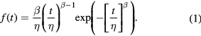
The tunnelling junctions were sequentially set under voltage at room temperature conditions. The current value was recorded for a time larger than the characteristic lifetime at that voltage level. The breakdown process is recognized by the formation of a short circuit. As example, a failure event for a junction with a MgO barrier thickness of 2.0 nm is shown in figure 2. In order to protect the measurement circuit, the maximal current value provided by the current source is limited to 20 mA. The inset shows the current values during the 300 s prior to the failure event. It is possible to recognize that the current level remains constant and no drift is observed, i.e. the breakdown process occurs in an abrupt way. This is always the case for the measured junctions.
Figure 2. Example measurement of a failure event for a tunnelling junction with a barrier thickness of 2.0 nm under a stress voltage level of 2.10 V. The breakdown of the barrier is recognizable by a strong increase of the current flowing through the element at t = 1110 s due to the formation of a shortcircuit. The inset shows in detail the current level evolution during 300 s before the failure event.
Download figure:
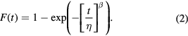
Standard image High-resolution imageFor the determination of each (η, β)-pair a MTJ population of about 20–25 members was used. Left panel in figure 3 shows exemplarily a typical measurement of the time evolution of the fraction F of failed elements for a population with a barrier thickness of 1.8 nm. For this particular measurement, the lifetime η is 72 s and the β parameter is  . The stress voltage level is 1.95 V. The error bar is calculated considering the population size of 23 elements. The red line represents the corresponding fit to equation (2). The Weibull distribution describes the time evolution of F very well and the small deviations are attributed to the finite size of the measured population.
Figure 3. Left: example measurement of the fraction F(t) of failed tunnelling junctions for a population with a barrier thickness of 1.8 nm with a stress voltage level of 1.95 V. Right: comparison of F(t) for data sets with different β values to prove the suitability of the Weibull cumulative function to describe the time evolution of the failure events. For visibility reasons the errors bars are omitted and the time axis is normalized to η to allow for comparison.
Download figure:
Standard image High-resolution imageIn order to further show the suitability of the used statistical model, three more cases are plotted in the right panel of figure 3. Here we show two extreme cases with the lowest and largest measured β values (0.54 and 2.11) together to a more common case. Since the data correspond to measurements with different time scales, the time axis is normalized to the η value to allow comparison. In all cases the model is able to describe the time evolution properly. With regard to the influence of the β parameter on the low infant mortality, we consider the F values after an elapsed time of  . For the case with
  the fraction of failed elements is as large as 34% while for
  is only 3.5%. For the intermediate case the corresponding value is 13%. For the left panel the fraction of failed elements increases up to 21%.
Since the stress agent is the electric field through the barrier, it is immediately clear that the characteristic lifetime η must scale with the voltage. On the contrary, if the failure mechanism is the same for all measured voltage levels, the β parameter should not vary. The opposite cases, i.e. a voltage-independent lifetime value or varying β parameter may hint to a defective measurement setup or very low quality tunnelling barriers for the first case, or heat induced effects or electromigration for the second.
For better comparison between different data sets, the use of Weibull plots is recommended. Applying the logarithmic function to (2) results in:

The use of Weibull plots is more convenient than plotting F(t) since they allow an easier comparison of all measurements at different voltages and time scales. Additionally, the linear behaviour can be recognized at first sight allowing for a fast optical check of measurement validity and proving the adequacy of the Weibull distribution. Furthermore, the slope in the graph is directly related to the β parameter. If the failure mechanism is voltage-independent, the slope should not be very different. The opposite case is not well described by the Weibull distribution.
Figure 4 exemplarily shows Weibull plots corresponding to different barrier thicknesses and RF deposition power. The scaling of the lifetime with the applied voltage is immediately recognized in the Weibull plots by a shift of the data sets for different values. The lines are a fit of (3) to the experimental data. The estimated slopes are similar for each plot although a certain scatter is unavoidable due to the finite size of the measured population. This shows that the breaking mechanism stays voltage independent for every barrier thickness value or deposition power.
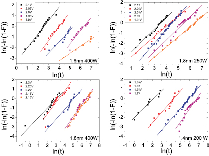
Figure 4. Weibull plots for different barrier thicknesses and RF deposition power showing that the slope (β) and thus the breaking mechanism stays voltage independent. The scaling of the lifetime with the applied voltage is immediately recognized in the Weibull plots by a shift of the data sets for different values. The lines are a fit of (3).
Download figure:
Standard image High-resolution imageAt this point, some conclusions can be obtained concerning the physical effects behind junction failure. Since the breaking mechanism is not depending on the applied voltage, and consequently also not on the current flowing through electrodes and barrier, the influence of degradation through electomigration can be discarded. The same conclusion is obtained for any degradation generated by temperature increase (interlayer diffusion) due to Joule heating. Indeed, the observation of only abrupt failure events (as shown in figure 2) with no previous drift is already indicating the same. Furthermore, the fact that for all cases the F(t) curve can be described with equation (2) points already to the dielectric breakdown as a single physical effect controlling the failure evolution. Electomigration or thermal damage is accumulating with time and would modify the F(t) evolution not allowing for a concordance with the Weibull cumulative function.
Typical working condition voltages for MTJs are much lower than the voltages used here (below 0.5 V). Since the lifetimes in the low voltage region can reach values well above 106 years, it is impossible then to get enough statistics in a reasonable measurement time. For this reason, the stress processes are accelerated by measuring at larger voltages. The open question now is the relation between the measured lifetimes at large voltages and the expected lifetimes at working conditions. In the literature several models are chosen, going from an inverse power law model to a more or less complicated exponential law [1, 4, 5, 9]. In our case, we choose a simple exponential dependence, which has been proven for Al2O3 [4, 5, 9] and MgO [10] tunnelling barriers:

Figure 5 exemplarily shows the measured dependence of the lifetime η on the applied voltage for a MTJ population with a 1.4 nm thick barrier. The error bar is provided by the linear fit to the corresponding Weibull plots. The line represents a fit to the exponential law shown in (4) describing the obtained results very well.
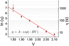
Figure 5. Dependence of the characteristic lifetime η of the tunnelling junctions and ln(η) on the stress voltage. The line is a fit to (4) for the estimation of the lifetime in the low voltage regime.
Download figure:
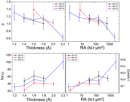
Standard image High-resolution imageThe obtained data is now summarized in figure 6. The top panels shows the dependence of the shape parameter β (average values for all voltages) on the barrier thickness and the resistance × area (RA) product for three wafer sets deposited with different RF power for the MgO process. The error bar is the result of the scatter of values for β for the different voltage values. Two main features can be recognized: first, the deposition power seems to have no influence on β, and, secondly, this parameter decreases continuously with the thickness (or RA product) of the MgO barrier. An important point has to be remarked here: with the exception of the case with a barrier thickness of 2.2 nm, all the values are larger than unity, i.e. we are in the situation with a low infant mortality and consequently high device reliability during the first operation stage. The bottom panels show now the dependence for the lifetime η in the low voltage regime. For visibility reasons, a logarithmic scale is used. The error bar is the result of the extrapolation of the linear fits to data sets as presented in figure 5 Here again the deposition power seems to have no influence although when only the graph with the nominal thickness is taken into account, slight differences may be recognized. The lifetime increases with increasing barrier thickness (or RA product). This is somehow intuitive since thicker barriers are more robust against breakdown processes. The overall absolute values for η are very large, pointing again to a very high reliability.
Figure 6. Dependence of the shape parameter β and the characteristic lifetime η in the low voltage regime (0.4 V) on the nominal thickness and the resistance × area (RA) product. For better visibility, a logarithmic scale is used for η and the RA product. For consistency reasons, ln(η) is calculated for η in seconds, as in figure 5.
Download figure:
Standard image High-resolution image
With the obtained (η, β) values it is possible to use (2) to calculate backwards the expected failure rate for our junctions after a certain elapsed time. The obtained values are below 1 ppm for most of the measured wafers after 10 years continuous operation. The possibility to obtain a prediction for the maximal failure rate of a MTJ during its expected operation time is of critical importance. It has to be taken into account that a real sensor is typically not based on a single junction but on different sets of MTJs in order to adjust resistance values or improve signal quality. The values obtained here also allow the calculation of these maximal failure rates for real sensors.
In order to analyze the influence of annealing on the lifetime properties, additional measurements were performed. Let us now compare the values of wafers with a barrier thickness of 1.4 nm annealed at 320 °C during 10 and 60 min with the as-deposited case. The following effects have been observed for the values of ln(η). For the non-annealed case, the maximum obtained value is  . The value for the wafer annealed for 10 min is
  , i.e. no real change is observed. For the wafer annealed during 60 min, the value increases to
  pointing to a slight improvement with annealing. The behaviour for β is very similar, the maximum value for non-annealed wafers is
  which is the same (
 ) for the 10 min annealed wafer. For the 60 min annealed wafer, a slight increase up to
  is observed. These results reveal that an annealing step may improve the lifetime characteristics of tunnelling junctions but the influence of the barrier thickness is much stronger.
The fact that annealing and the deposition power have a reduced effect on the failure properties points to the barrier thickness as the main parameter. This is again compatible with dielectric breakdown being the sole responsible for junction failure.
In summary, a study of the influence of the barrier thickness and the RF deposition power on the lifetime characteristics of MgO based tunnelling junctions has been performed. To the knowledge of the authors such study has not been previously reported. The obtained data demonstrates the suitability of the Weibull distribution for analysis of MgO based tunnelling junctions and a voltage independent failure mechanism at room temperature dielectric breakdown processes. Dielectric breakdown processes are concluded to be the single physical effect controlling the failure time evolution. The data excludes any possible influence of electromigration or thermal effects in the measured junctions. A strong increase of the characteristic lifetime η with increasing barrier thickness has been observed while the β parameter shows the opposite trend. The RF deposition power has a very limited influence.
The large η values and the observation of β values larger than 1 prove a large reliability and small infant mortality for the investigated junctions. The maximum calculated failure rates projected for a 10 years operation are smaller than 1 ppm.
The effects of an annealing step have been tested revealing only a slight improvement in the characteristics compared to the as-deposited state, proving that the thickness of the barrier is the main parameter.
Acknowledgments
Financial support by the state of Rhineland-Palatinate (MBWWK and MWKEL) and by the European Regional Development Fund (ERDF) in the frame of the Spintronic Technology Platform (STeP) is acknowledged. The authors thank S Eilers and M Bürkle for their technical support at Sensitec.