

Abstract
Organic thin films have numerous advantages over inorganics in device processing and price. The large polarization of the organic ferroelectric oligomer vinylidene fluoride (VDF) could prove useful for both device applications and the investigation of fundamental physical phenomena. A VDF oligomer thin film vacuum deposition process, such as thermal evaporation, preserves film and interface cleanliness, but is challenging, with successful deposition occurring only within a narrow parameter space. We report on the optimal deposition parameters for VDF oligomer thin films, refining the parameter space for successful deposition, resulting in a high yield of robust ferroelectric films. In particular, we investigate the influence of deposition parameters on surface roughness, and the role that roughness plays in sample yield. The reliable production of ferroelectric films allowed us to perform detailed measurements of previously unreported properties, including the Curie temperature, the temperature and thickness dependence of the coercive field, the melting temperature, and the index of refraction. The ability to successfully grow robust, switchable, well-characterized films makes VDF oligomer a viable candidate in the field of organic ferroelectrics.
Export citation and abstract BibTeX RIS
Introduction
Organic thin films form an integral part of technologically important devices, including field-effect transistors [1], organic light emitting diodes [2], solar cells [3–5], antireflection coatings [6], and magnetic field sensors [7]. Organic thin films also offer advantages in the investigation of fundamental scientific phenomena, including spin transport [8] in magnetic tunnel junctions [9, 10] and ferroelectric tunnel junctions [11]. Organic ferroelectric thin films have proved useful in the investigation of electric-field control of magnetism, an effect that is of major interest [12–14], because of both the fundamental physics behind magnetoelectric effects and the technological implications of such control. The latter includes the advancement of spintronic devices, magnetic field sensors, and non-volatile magnetic memory storage devices. Electric-field control of magnetic properties has been observed in a wide variety of materials [15–20], with the mechanism highly dependent on the choice of materials. Magnetoelectric coupling in layered ferroelectric/ferromagnetic thin film heterostructures typically arises from volumetric effects, coupling magnetic and electrical order via strain [21–23]. Other subtle interfacial effects, such as the spin dependent screening potential [24, 25] that arises from electric field penetration, can result in changes in the magnetic anisotropy and/or magnetization, but are typically overshadowed by volumetric effects. Theoretical modeling of the magnetoelectric coupling between organic ferroelectric thin films of poly(vinylidene fluoride) (PVDF) and metallic ferromagnetic thin films predict large changes in the magnetic anisotropy of the ferromagnetic film [26], an effect that was clearly seen in experiments on heterostructures of the copolymer poly(vinylidene fluoride-trifluoroethylene) (P(VDF-TrFE) with a 70 : 30 ratio of VDF to TrFE) and a ferromagnetic Co thin film [15]. In these heterostructures, volumetric effects play a minor role at best because of the large mismatch in stiffness coefficients.
Ferroelectric VDF oligomer is particularly well suited for experiments on the electric-field control of magnetism because of its low stiffness coefficient [15] (~100 times softer than a typical metal) and its high remanent polarization [27] of 0.13 C m−2 (as compared to 0.06 C m−2 for PVDF [28]). The large surface charge density results in a large effective electric field at the ferroelectric/ferromagnetic interface and the low stiffness ensures that changes in magnetic behavior are due to the electric field and not to strain coupling, essentially minimizing the volumetric effects present in other ferroelectric/ferromagnetic systems. In addition, the shorter, well-defined chain lengths of the oligomer, as compared to the polymer PVDF, will lead to better crystallinity and easier nanoscale processing.
If VDF oligomer is to be used in a ferroelectric/ferromagnetic heterostructure, such as the magnetic tunnel junctions described in Refs. [9] and [10], ferroelectric tunnel junctions like those described in Ref. [11], or in other nanostructured devices, a clean, well-characterized contact between the organic layer and any adjacent layers is imperative. This requirement eliminates Langmuir-Blodgett deposition or solvent spin coating as possible deposition techniques since these processes expose the sample to the atmosphere during the deposition and compromise the cleanliness of the electrode/oligomer interface. An all-vacuum deposition of the heterostructure, in particular thermal evaporation of the VDF oligomer layer, will result in clean, abrupt, and well-defined interfaces. Unfortunately, thermal evaporation of VDF oligomer in the requisite ferroelectric β-phase and with the appropriate crystalline orientation can be difficult due to a demanding set of deposition parameters [29]. Previous reports on the growth of ferroelectric thin films of VDF oligomer by vacuum evaporation indicate a range of deposition rates and define the optimal substrate temperatures for growing films of the appropriate phase and orientation but provide few other insights on how to grow high quality fims [27, 30–33]. Furthermore, although some physical and ferroelectric properties of VDF oligomer thin films, such as the remanent polarization [27], pyroelectric coefficient [31], and structure of epitaxially grown films [34, 35] have been reported, many other properties remain unreported. To that end, the objectives of this work are twofold: first, we provide a comprehensive study of the thermal evaporation of VDF oligomer thin films that offers insight into parameter control for the successful growth of the films, and second, we report on several properties of the resulting VDF oligomer thin films.
Experiment
VDF oligomer thin films can be categorized and differentiated by their chain conformations, with the most common forms being β-phase (form I), α-phase (form II), or γ-phase (form III) [36]. The conformations result in different crystallographic structures that can be identified by x-ray diffraction (XRD). Both α-phase and γ-phase crystals have no net polarization due to the antiparallel configuration of neighboring dipole moments, making their presence undesirable for our purposes. The all-trans conformation of the β-phase, shown in figure 1, results in a net dipole moment perpendicular to the molecular c axis along the (0 2 0) direction and is ferroelectric. The direction of the polarization is also important for device application. Any device using a stacked electrode structure similar to that shown in figure 1 requires at least some component of the polarization perpendicular to the plane of the electrodes. Noda et al have studied the structure of VDF oligomer films as a function of substrate temperature during deposition in some detail [34, 35]. Using grazing-incidence XRD, Fourier-transform infrared spectroscopy, and atomic force microscopy (AFM), they found that the crystalline phase is highly dependent on substrate temperature, and grows epitaxially on substrates such as KCl (0 0 1). Ultimately, it was found that β-phase crystals dominate the thin film when deposited on any substrate, regardless of crystalline order, at low deposition temperatures close to 130 K. This insight informs the present work—all the thin films described here were deposited at a fixed substrate temperature of 128 K.
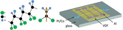
Figure 1. (Left) VDF oligomer structure. The β-phase chain conformation shown results in ferroelectric ordering. (Center) An electric dipole moment forms across the carbon chain, directed from the highly electronegative F atoms to the H atoms. (Right) Sample structure: glass (1 mm)/Pt (50 nm)/Co (1.2 nm)/VDF (t nm)/Al (20 nm). The Al and Pt/Co layers serve as top and bottom electrodes respectively.
Download figure:
Standard image High-resolution imageThe thin films of VDF oligomer [CF3-(CH2CF2)n-I] (shown in figure 1) were deposited in a thermal evaporation chamber connected via a gate valve to a sputtering/e-beam evaporation chamber [29]. VDF oligomer powders from two separate manufacturers, Kunshan Hisense Electronic Co., Ltd. and Daikin Industries, Ltd., were used with no apparent difference in film quality. The Kunshan Hisense oligomer had a chain length of n = 15 ± 2, as measured by nuclear magnetic resonance spectroscopy, while the Daikin Industries oligomer has a chain length of n = 14 ± 1, as measured by mass spectrometry. Metallic electrodes were deposited in the adjacent sputtering/e-beam chamber, allowing the samples to be made without removing them from vacuum, resulting in clean oligomer/metal interfaces. Most samples consist of glass (1 mm)/Pt (50 nm)/Co (1.2 nm)/VDF (t nm)/Al (20 nm), with t ranging from 50 nm to 2500 nm. Figure 1 shows a typical sample structure with the Pt/Co and Al electrodes enclosing a device area of 0.04 mm2. Here, the Pt/Co layer merely serves as a metallic electrode; the ferromagnetic properties of the Co are not relevant because this work is primarily focused on the optimal growth and characterization of the VDF oligomer. The base pressures of the sputtering/e-beam chamber and the organic thermal evaporation chamber were 1 × 10⁻⁸ Torr and 8 × 10⁻⁸ Torr respectively. The metallic electrodes were deposited at a rate of 0.2–0.5 Å s−1, and the VDF oligomer was grown at deposition rates varying between 1.14 Å s−1 and 11.7 Å s−1, as determined by spectroscopic ellipsometry measurements. The deposition rate of the VDF oligomer was controlled by varying the current through the filament in the evaporator's effusion cells [29], which were equipped with thermocouples to monitor the temperature of the VDF oligomer crucible during the deposition. The crucible temperature was shown to be an important parameter in obtaining switchable, ferroelectric films (discussed below). The VDF oligomer begins to evaporate, albeit at a low rate, at a crucible temperature of 30 °C [29]. Because we were interested in optimizing the yield of switchable, ferroelectric films, we made and measured a total of 87 VDF oligomer thin film samples, each with multiple metallic electrodes similar to that shown in figure 1. Multiple electrode areas on the same sample differed only in VDF oligomer film thickness (detailed in figure 5), allowing for control of all other variables. In addition to the samples on glass substrates, 22 VDF oligomer thin film samples were grown on polished Si wafers using the same deposition conditions as samples on glass substrates outlined above. These Si/VDF oligomer samples were used exclusively for XRD and spectroscopic ellipsometry measurements, the details of which are outlined below.
XRD measurements on all 22 Si/VDF oligomer thin films samples were made in θ–2θ mode using a Rigaku D/Max-B Diffractometer with Co Kα radiation of wavelength 1.789 Å. AFM measurements were made on 27 of the thin film samples on glass substrates using a Digital Instruments Nanoscope IIIa Dimension 3100 SPM system in tapping mode at a frequency of 138 kHz. Pyroelectric measurements were made on all 245 electrodes of the 87 thin film samples on glass substrates using the Chynoweth method [37] with a 1 mW, 658 nm wavelength diode laser modulated at 2 kHz. The film thickness and optical properties of 5 Si/VDF oligomer thin films samples were determined by ellipsometry measurements [38, 39] using a J.A. Woollam M-2000 DI spectroscopic rotating compensator ellipsometer. The dependence of the refractive index on wavelength was modeled by a Cauchy dispersion equation in the spectral range of 300 to 1700 nm using CompleteEASE® software available through the J.A. Woollam Company. Maps of film thickness and refractive index were recorded using spectroscopic ellipsometry with a beam diameter of 300 μm by measuring 81 points in a sample area measuring 1.5 cm by 1.5 cm.
Results and discussion
Following the work of Noda et al the films discussed here were deposited on liquid-nitrogen-cooled substrates, at a temperature of 128 K, resulting in a large fraction of β-phase VDF oligomer. This crystallographic orientation is apparent from the XRD data, shown in figure 2, for the as-grown thin film. A two-peak fit to the data results in peaks at 2θ = 23.1° and 23.8°, which correspond to the (1 1 0) peak of the α-phase and the (0 2 0) peak of the β-phase, respectively [40, 41]. Figure 2 shows that the as-grown VDF oligomer thin films are predominantly in the (0 2 0) β-phase, the optimal orientation for maximum out-of-plane polarization. Annealing results in a larger proportion of (1 1 0) β-phase, but does not result in a significant improvement in the crystallinity (discussed below). We note that the longer wavelength radiation from the Co Kα source used here (as compared to the more common Cu Kα radiation with wavelength 1.54 Å), allows for a clear separation between these closely spaced diffraction peaks. Hence, we can clearly distinguish between (1 1 0) and (0 2 0) β-phase peaks, whereas previous measurements could not [32], allowing us to say definitively that the as-grown films are oriented along the (0 2 0) direction.
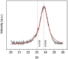
Figure 2. XRD data for the as-grown VDF oligomer thin film. No significant changes are observed in the XRD data as deposition parameters were varied, indicating that as long as the substrate is cooled during deposition, the as-grown film is predominantly in the (0 2 0) β-phase. A two-peak fit is shown in red.
Download figure:
Standard image High-resolution imageXRD measurements were performed on samples grown under various sets of deposition parameters. Using the Scherrer equation
where k is the shape factor, widely accepted as 0.9, λ is the wavelength of the radiation, β is the full width at half maximum value of the Bragg peak, and θ is the location of the Bragg peak, we calculate τ, the average particle size of the VDF oligomer thin films. Calculated Scherrer particle sizes of the majority (0 2 0) β-phase varied little, ranging from 14.6 nm to 15.4 nm, and show no correlation with deposition rate, crucible temperature, or film thickness.
Although all films showed diffraction peaks similar to that in figure 2 and possessed a measureable pyroelectric current, indicating the presence of β-phase VDF oligomer, it was found that merely keeping the substrate cooled during deposition is not sufficient for successful growth of ferroelectric, switchable VDF oligomer thin films. Successful VDF oligomer growth, defined by the ability to saturate the ferroelectric polarization and switch its direction, i.e. collect a complete pyroelectric hysteresis loop, was found to be highly dependent on the surface roughness of the thin film. The surface roughness is governed by the deposition rate, which in turn is controlled by the crucible temperature. Initial attempts, in which the crucible temperature was allowed to rise as high as 80 °C, resulted in a poor yield of less than 25%, though minor polarization hysteresis loops were often obtained. Although nearly every sample showed a strong pyroelectric current (even at low applied voltage) less than 25% of the samples could withstand a voltage large enough to saturate and/or switch the sample. In an effort to increase the yield of switchable, ferroelectric films, we first investigated the surface roughness of the VDF oligomer thin film. Our data on the role of roughness are summarized in figures 3 and 4.
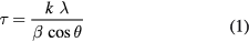
Figure 3. AFM measurements, photographs, and pyroelectric hysteresis loops from rough and smooth samples. The data in the left column along with the black hysteresis loop corresponds to rough samples, grown at high deposition rates (11.7 Å s−1). The data in the right column along with the red hysteresis loop corresponds to smooth samples, grown at low deposition rates (1.14 Å s−1). (a) and (b) AFM measurements, showing a dramatic increase in surface roughness as deposition rate is increased. (c) Photograph of irreversible damage suffered by a rough sample after the application of voltage. (d) Photograph of a smooth sample after 15 polarization reversals showing no damage. The inset shows a smooth sample driven to failure via the application of large voltage. (e) Pyroelectric hysteresis loops of otherwise identical rough and smooth samples.
Download figure:
Standard image High-resolution image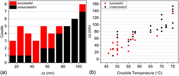
Figure 4. (a) Histogram showing the numbers of successful and unsuccessful samples as a function of maximum peak-to-valley distance, Δz. The last bin represents all Δz values greater than 100 nm. (b) Δz as a function of crucible temperature during deposition. Figures 4(a) and (b) together reveal the optimal deposition conditions to maximize yield.
Download figure:
Standard image High-resolution imageFigure 3 shows AFM and optical images of evaporated VDF oligomer thin films. Each column corresponds to distinct samples grown under identical growth conditions. The data in the left column, figures 3(a) and (c), along with the black pyroelectric hysteresis loop in figure 3(e), were taken on samples grown at high crucible temperatures (75 °C) corresponding to high deposition rates (11.7 Å s−1). In contrast, the data in the right column, figures 3(b) and (d), along with the red hysteresis loop in figure 3(e) were taken on samples grown at low crucible temperatures (48 °C) corresponding to low deposition rates (1.14 Å s−1). The AFM images in figures 3(a) and (b) were recorded on the VDF oligomer thin films prior to the deposition of a top electrode and show that the films grown at high deposition rates have a higher root-mean-square (rms) roughness (20 nm versus less than 5 nm) and a larger maximum topographical peak-to-valley distance, Δz, than those grown at low deposition rates. Samples grown at a high deposition rate suffer electrical breakdown after only a few (usually no more than two) polarization switches. In contrast, samples grown at a lower deposition rate survive the application of poling voltage and repeated polarization switching. Figure 3(c) is a true color photograph of a rough, high deposition rate sample taken through an optical microscope that shows irreversible damage appearing on the surface of the electrode after the first application of voltage. Figure 3(d) is a photograph of a smooth, low deposition rate sample that shows no significant damage, even after 15 polarization reversals. These differences only appear subsequent to voltage application. Although both rough and smooth films can be made to fail, the inset of figure 3(d) shows a smooth sample that was intentionally destroyed by applying high voltage (>100 V), much higher than that necessary to saturate the sample. Clearly, the electric field induced damage at the surface of the smooth sample is different than that suffered by the rough sample, indicating that the failure modes for rough and smooth samples are different.
Pyroelectric measurements on the few rough samples that do survive the application of voltage show that surface roughness does not correlate with the ferroelectric properties of VDF oligomer thin films, as demonstrated in figure 3(e). This figure shows nearly identical pyroelectric hysteresis loops from two samples with identical thicknesses and areas even though one (black data) was much rougher than the other (red data). Rather, the role of roughness manifests itself in whether or not the sample can survive the application of voltage. The Al top electrode conforms to the topography of the VDF oligomer layer below it, so a rough VDF oligomer layer will cause large electric field variations across the electrode area at constant voltage, resulting in damage to the VDF oligomer and subsequent failure. The role of roughness in the successful growth of ferroelectric, switchable VDF oligomer films is summarized in figures 4(a) and (b). The histogram in figure 4(a) quantifies the role of maximum peak-to-valley distance, Δz, in successful sample yield for the subset of samples on which both AFM and pyroelectric measurements were made. The bins span 10 nm in Δz, with the last bin representing all Δz values greater than 100 nm. Each count represents one electrode from these samples, with red representing an electrode area on which a complete pyroelectric hysteresis loop was successfully obtained and black representing a failed electrode. As Δz approaches 70 nm, the yield rate falls significantly. Figure 4(b), in turn, relates crucible temperature to Δz for this same subset of samples showing that a crucible temperature between 50 °C and 60 °C is ideal. Depositions at very low crucible temperatures (40 °C or lower) were also attempted, but no pyroelectric current was measured on these samples regardless of surface roughness. Trace amounts of highly fragmented VDF oligomer chains were detected by mass spectrometry, and it is thought that at these low temperatures, only light fragments are deposited on the substrate.
With this newly refined parameter space for the growth of high quality ferroelectric thin films of VDF oligomer, we restrict ourselves to the production of these smooth (low deposition rate), switchable, robust films, and probe the physical properties of these VDF oligomer films. Given the growing general interest in using organic thin films in optical devices [2–6], we first report on the refractive index of VDF oligomer thin films. Using a spectroscopic ellipsometer, a technique that has already been used to successfully probe the optical properties of P(VDF-TrFE) films [42, 43], the large-scale topographical and optical properties of VDF oligomer thin films are investigated, with typical results shown in figure 5. The VDF oligomer films show uniaxial anisotropy, where the optical axis is perpendicular to the film surface. Figure 5(a) shows the ordinary (in-plane) index of refraction of a VDF oligomer thin film on Si over a sample area measuring 1.5 cm by 1.5 cm. The value of the refractive index at a wavelength of 632.8 nm is 1.42 with a small variation of ±0.012 (and a standard deviation of 0.004) across the full sample area. The relatively small variation in the index of refraction indicates a uniform film density. Furthermore, this value changes little as film deposition parameters are changed. We have been unable to find values for the refractive index of the VDF oligomer in the literature, though the refractive index for PVDF polymer films ranges from 1.42 to 1.52 [44–46]. The consistency of the index of refraction for VDF oligomer films measured from several samples indicates that regardless of deposition conditions, the density of the VDF oligomer film remains largely uniform, at least over the length scales of the measurement (300 μm). Spectroscopic ellipsometry also allows for the calculation of film thickness along with the index of refraction. Figure 5(b) shows a thickness map across the same sample area. Here, 0 nm on the vertical axis corresponds to the Co/VDF interface. The film thickness follows the expected 1/r2 dependence [47], where r is the distance between the sample and the source during deposition, as shown by the fit in the inset. Although the VDF oligomer thickness is not uniform across large areas, over small electrode areas the thickness will be approximately uniform. For example, for the sample shown in figure 5(b), the VDF oligomer thickness would change by only 1 nm across the 0.2 mm-wide electrode. More detail on the modeling of our ellipsometry data can be found in the supplemental material accompanying this work while references 38, 39, 42, and 43 provide an in-depth discussion on the topic (stacks.iop.org/JPhysD/49/015301/mmedia).

Figure 5. (a) Map of the ordinary component of the index of refraction over a large area for a VDF oligomer thin film measured using ellipsometry. The top left corner corresponds to the edge of the sample. (b) VDF oligomer film thickness map across the same area. The inset is a cross section of this map with a 1/r2 fit in red.
Download figure:
Standard image High-resolution imageNext, to determine the Curie temperature of these VDF oligomer thin films, the pyroelectric current is measured as a function of film temperature. The pyroelectric current, Ip, is given by [37]:
where, A is the area of the electrode, dP/dT is the change in spontaneous polarization with temperature, and dT/dt is the rate of change of temperature. Experiments by Noda et al on VDF oligomer thin films show that the detected current is dominated by the pyroelectric current and that any non-pyroelectric, temperature-dependent generated current is small in comparison [31]. Using the Chynoweth method and following the discussion in reference 37, dT/dt can be taken as a constant for a given light intensity. The pyroelectric current, then, is proportional to the slope of the polarization curve with temperature, dP/dT. The slope of the P versus T curve for a ferroelectric increases close to the Curie temperature and is a maximum at that temperature. Because the ferroelectric transition is first order [48, 49], there exists a finite temperature range near the transition temperature in which both the ferro- and paraelectric phases coexist. In this coexistence regime, the pyroelectric electric current does not instantaneously drop to zero once the transition temperature has been reached. Rather, the current should increase as the transition temperature is approached and then decrease over a finite temperature range close to the transition temperature, which is exactly the temperature dependence we observe in figure 6. This figure shows the measured pyroelectric current of a saturated 500 nm thick VDF oligomer thin film at zero applied voltage as a function of temperature. The temperature was raised from 19 °C to 90 °C at a rate of 3 °C min−1. (This method has been previously used to determine the transition temperature, 88 °C, in Langmuir-Blodgett deposited P(VDF-TrFE 70:30) thin films [50].) For the sample shown in figure 6, the magnitude of the pyroelectric current at room temperature, subsequent to this heating cycle, is only 14% of its original value prior to heating. Saturating the sample, with the application of 60 V across the VDF oligomer thin film, increases the magnitude of the pyroelectric current to 40% of its original value. From these data, we conclude that the Curie temperature for these films is 61 °C, and that the film partially depolarized and suffered damage upon further heating to 90 °C.
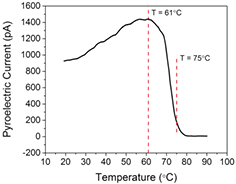
Figure 6. Pyroelectric current as a function of temperature. The pyroelectric current rises with temperature until the film reaches 61 °C. With increasing temperature, the current decreases as the film transitions from the ferro- to paraelectric phase, going to zero at 80 °C.
Download figure:
Standard image High-resolution imageTo investigate the film damage mechanism at temperatures above the transition temperature, an optical microscope movie was made of the effects of temperature on VDF oligomer thin films, showing a dramatic change in the film at a temperature close to 75 °C (second dotted line in figure 6). Still frames from this movie are shown in figure 7, and the entire movie is available online in the supplemental material accompanying this work (stacks.iop.org/JPhysD/49/015301/mmedia). From the movie, we determined that the film begins to melt at 75 °C. The bubbles in the film shown in figure 7 remain even when cooled to room temperature, which, along with the decrease in pyroelectric current at saturation, indicates that permanent structural damage occurs in the film upon melting. Earlier differential scanning calorimetry measurements [51] on VDF oligomer powders with the same end groups as those used here indicate a melting temperature of 95 °C for chain length n = 14. This difference may be attributable to thin film growth, as earlier results on vapor deposited thin films [52] of VDF oligomer (albeit with different end groups) showed a substantially lower melting temperature of thin films as compared to powders, with a difference that is highly dependent on crucible temperature.
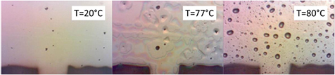
Figure 7. Still frames from a movie of a VDF oligomer thin film on a Pt/Co electrode being heated. For reference, the movie is taken at the location where the thin strip (bottom of the still frame) meets the square pad (see figure 1) of the bottom electrode. The film undergoes a dramatic change around 75 °C. At 80 °C, the pyroelectric signal disappears and bubble-like features appear on the surface of the film and remain even after the film is cooled back down to room temperature.
Download figure:
Standard image High-resolution imageThe data in figures 6 and 7 indicate there is a narrow temperature range, above the ferroelectric transition and below the melting temperature [53], that is suitable for annealing. VDF oligomer films were annealed in air at 68 °C for 90 min, with ramp times of 90 min for both increasing and decreasing temperature. The effects of annealing were analyzed via XRD measurements and the results are shown in the top two panes of figure 8. Before annealing, the (0 2 0) β-phase VDF oligomer (2θ = 23.8°) was dominant, with no (1 1 0) β-phase VDF oligomer (2θ = 24.4°) detected. After annealing, however, the (1 1 0) β-phase is dominant, with a 20 : 1 ratio of (1 1 0) to (0 2 0) β-phase, while the total area under all peaks remained constant. Calculated Scherrer particle sizes, in this case for the majority (1 1 0) β-phase, are similar to those from the majority (0 2 0) β-phase before annealing, ranging from 13.5 nm to 14.0 nm. Similar to Langmuir-Blodgett deposited PVDF thin films, however, annealing these VDF oligomer thin films caused no appreciable change in the observed pyroelectric hysteresis loops. This behavior is not surprising, because the ferroelectric polarization is directed along the (0 2 0) direction. Polarization measurements along the (1 1 0) direction will result in only a 13.4% reduction in the out-of-plane component of polarization since the ferroelectric polarization is canted 30° away from the (1 1 0) direction. We conclude that annealing is unnecessary, because it decreases the out-of-plane polarization and does not improve the crystallinity.

Figure 8. Room temperature XRD data (from top to bottom) for an as-grown, unannealed VDF oligomer thin film, after annealing at 68 °C for 90 min, after heating at 75 °C, after heating at 98 °C, and for a blank Si substrate for reference. Annealing clearly increases the proportion of (1 1 0) to (0 2 0) β-phase VDF oligomer in the film. The insets are photographs of the melted films after cooling. Note that the vertical axes in the third and fourth panes are multiplied by a factor of five.
Download figure:
Standard image High-resolution imageBecause the reduction in pyroelectric current upon heating described above may result from sample melting, phase changes, or perhaps even from evaporation of the film off the substrate, room temperature XRD measurements were taken on VDF oligomer thin film samples heated to different temperatures, with the results shown in the middle panes of figure 8. Heating to 75 °C, results in a substantial decrease (by a factor of 60) of the area under the peak corresponding to the (1 1 0) orientation of the β-phase. This peak disappears entirely upon heating to 98 °C, well past the melting temperature. However, the peaks for the non-ferroelectric (1 1 0) α-phase and the (0 2 0) β-phase, at 2θ = 23.1° and 23.8° respectively, are still present, albeit reduced in area. The reductions in the areas under these peaks are much less pronounced than that of the (1 1 0) β-phase peak: heating to 75 °C reduces the areas under the (1 1 0) α-phase and (0 2 0) β-phase peaks by a factor of 3, while heating to 98 °C results in a further reduction of 1.3. The total area under all the peaks, a measure of crystallinity, decreases by a factor of 24 after heating to 75 °C, and by an additional factor of 2 when heating to 98 °C, indicating a loss of crystallinity. The insets in the middle panes of figure 8 show optical microscopy photographs of the samples corresponding to the XRD data after cooling back to room temperature. In addition to the (1 1 0) β-phase VDF oligomer peak completely disappearing after raising the film's temperature to 98 °C, the bubble-like features have completely disappeared as well. Films heated to this temperature show no pyroelectric current after cooling to room temperature. However, films heated to 90 °C still showed some pyroelectric current upon cooling and re-saturation (see discussion on figure 6 above), which we can now attribute to the small remaining fraction of (0 2 0) β-phase VDF oligomer. The persistence of the preferred (0 2 0) β-phase peak may be attributed to partial recrystallization upon cooling. Clearly the fraction of the material that recrystallizes in this fashion is small. It is possible, but unlikely, that the material recrystallizes into a higher index orientation on cooling. Another, more likely possibility is that the VDF oligomer evaporates away from the substrate when heated to these high temperatures. The exact details of the process remain an open question.
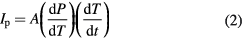
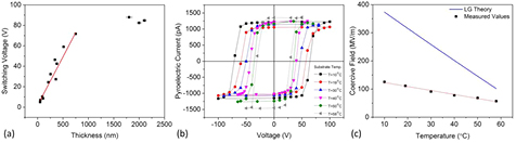
Finally, the ferroelectric coercive field, Ec, of evaporated VDF oligomer thin films was measured as a function of film thickness and temperature. The switching field is an intrinsic material property and should not vary with deposition parameters such as thickness and deposition rate. The observed extrinsic field, however, often differs from the predicted intrinsic field due to domain nucleation. Previously reported values of Ec for VDF oligomer thin films range from 75 MV m−1 to 120 MV m−1 at room temperature [27, 31, 33] and in one case was as high as 300 MV m−1 [35]. Figure 9(a) shows the switching voltage for VDF oligomer thin films (both annealed and unannealed since there is no appreciable difference) as a function of film thickness, with error bars calculated from the known 1/r2 thickness variation (see above). The switching voltage increases linearly with thickness in the submicron regime, but eventually saturates for films thicker than ~1 μm. This behavior is in line with expectations, where an increase in thickness results in a higher density of defects and increases the likelihood of domain nucleation. A linear fit to the data in the submicron regime indicates a coercive field of 95 MV m−1, in line with earlier measurements. The temperature variation of the hysteresis loops is shown in figure 9(b) on an annealed sample with a total thickness of 510 nm, and show a decrease in the switching voltage, Vc, as film temperature increases. Figure 9(c) shows the coercive field, Ec, calculated from Vc taken from the right side of each hysteresis loop in figure 9(b). The coercive field decreases as film temperature increases, which is indeed the expected behavior and in good agreement with similar measurements taken on P(VDF-TrFE 70:30) thin films [54, 55]. We perform a cursory comparison of our results to the intrinsic coercive field predicted by the Landau-Ginzburg (LG) mean-field theory given by [55]:

Figure 9. (a) VDF oligomer thin film switching voltage as a function of film thickness. The linear fit (red line) indicates a coercive field of 95MV m−1. (b) VDF oligomer thin film pyroelectric hysteresis loops for various film temperatures. (c) Coercive field measurements as a function of temperature. The red line is a linear fit to the measured data, while the blue line is the calculated coercive field given by equation (3).
Download figure:
Standard image High-resolution image
Here, t = 4α0(T–T0)γ/β2 is the reduced temperature, and T0 = Tc–3β2/16α0γ. The LG free energy coefficients α0, β, and γ are independent of temperature. For this cursory check we use the values of α0, β, and γ that are used for P(VDF-TrFE) [55]: α0 = 7.5 × 10⁷ JmC−2 K−1, β = −1.9 × 10¹² Jm5C−4, and γ = 1.9 × 10¹⁴ Jm9C−6. Taking Tc = 61 °C and using the values of the LG free energy coefficients above gives T0 = 13.5 °C. The blue line in figure 9(c) is the calculated intrinsic coercive field using equation (3), and has a slope approximately four times higher than the linear fit of the measured extrinsic field. The discrepancy between the calculated values for the intrinsic field and the measured coercive fields may be reduced by using the as-yet unknown LG free energy coefficients for the VDF oligomer, but are unlikely to reduce it enough to match the measured field. This mismatch is not surprising because we are unlikely to measure the intrinsic field at this large thickness. However, LG mean-field theory does predict the monotonic decrease in coercive field with temperature that we measure.
Conclusion
Ferroelectric organic oligomers such as VDF oligomer are attractive alternatives to both conventional oxide materials and ferroelectric polymers. We have investigated and optimized thermal evaporation of VDF oligomer, resulting in the ability to reliably and reproducibly grow organic ferroelectric thin films of the appropriate phase and orientation in a clean vacuum environment, necessary for producing pristine and well-characterized interfaces.
Extensive XRD, AFM, ellipsometry, and pyroelectric measurements have allowed us to define the parameters for successful VDF oligomer thin film deposition, maximizing the proportion of the ferroelectric β-phase with out-of-plane polarization. The highest yield of successful films is obtained for substrate temperatures at or below 130 K and crucible temperatures between 50 °C and 60 °C which correspond to a low deposition rate (below 2.0 Å s−1) which in turn minimizes film roughness. The maximum peak-to-valley distance, as obtained from AFM measurements, must be below 70 nm. A post deposition anneal at 68 °C for at least 90 min results in a high proportion of the (1 1 0) to (0 2 0) β-phase without damaging the sample. We conclude that post annealing is unnecessary, since the largest out-of-plane polarization occurs for the orientation of the as-grown films.
The growth of high quality films allowed for measurements of the properties of VDF oligomer thin films, many of which have not been previously reported. Among these properties are the ferroelectric Curie temperature of 61 °C and the index of refraction. Ellipsometry measurements show that the index of refraction at λ = 632.8 nm is n = 1.42 with very little variation, whether across a single film or between films grown under very different deposition conditions. This value is comparable to, but more consistent than, the refractive index of PVDF films, which range between 1.42 and 1.52. Temperatures above 75 °C result in permanent structural damage due to melting with complete destruction occurring at 98 °C. Extensive pyroelectric hysteresis measurements reveal that the coercive field at room temperature for VDF oligomer films in the submicron regime is fairly constant at 95 MV/m. The temperature dependence of the coercive field follows the expected behavior (decreasing with increasing temperature) as predicted by LG mean-field theory.
In conclusion, we have shown that the VDF oligomer is a strong candidate for use as a vacuum deposited ferroelectric thin film, mapped its deposition parameter space, and reported on its physical properties, increasing the viability of VDF oligomer thin films as a channel to explore new physics and develop new devices based on organic electronics.
Acknowledgments
Financial support is provided by the National Science Foundation (NSF) (Grant No. ECCS-1101256). Funding for C. L. was provided by an Undergraduate Creative Activities and Research Experience (UCARE) grant from UNL. Funding for M.S. was provided by the NSF through Nebraska Materials Research Science and Engineering Center (MRSEC) (Grant No. DMR-1420645). Research was performed in part in facilities of the Nebraska Center for Materials and Nanoscience which is supported by the Nebraska Research Initiative. The authors would like to thank M Foreman for help with photography and videography.