

Abstract
Tungsten doped tin oxide thin film transistors (TWO-TFTs) were fabricated by radio frequency magnetron sputtering. With TWO thin films as the channel layers, the TFTs show lower off-current and positive shift turn-on voltage than the intrinsic tin oxide TFTs, which can be explained by the reason that W doping is conducive to suppress the carrier concentration of the TWO channel layer. It is important to elect an appropriate channel thickness for improving the TFT performance. The optimum TFT performance in enhancement mode is achieved at W doping content of 2.7 at% and channel thickness of 12 nm, with the saturation mobility, turn-on voltage, subthreshold swing value and on–off current ratio of 5 cm2 V−1 s−1, 0.4 V, 0.4 V/decade and 2.4 × 10⁶, respectively.
Export citation and abstract BibTeX RIS
Introduction
Oxide thin film transistors (TFTs) have been widely studied for more than one decade since reported in Science and Nature magazine. Due to high electron mobility, high transparency, high uniformity, and low processing temperature [1, 2], they have become the most competitive candidate for next generation flat panel display. So far, many indium oxide based channel layer materials have been developed, such as In2O3 [3], InGaO [4], InSiO [5], InZnO [6], InWO [7], InGaZnO [2], InZnSnO [8], InZnWO [9]. Among them, a-IGZO material is widely investigated and has been put into industrial production. Nevertheless, the abundance of the earth's indium element is just 0.05 ppm [10], and the increasing electronic and photoelectric market demand lead to the increasing price by a factor of approximately ten [11]. Therefore, developing novel indium free oxide channel materials for high performance and low cost oxide-TFTs is necessary. It is believed that amorphous semiconductors constituting of metal cations with an electronic configuration (n − 1)d10ns0 have large electron mobilities, such as In3+(4d105s0), Sn4+(4d105s0), Zn2+(3d104s0). Compared with local and extended anisotropic silicon p or d orbitals, the spherical symmetry of indium cation s orbitals make electronic transport less sensitive to atom location [2, 12]. Therefore, tin oxide can be one of the most promising alternatives to indium oxide for amorphous oxide TFT. However, compared with other oxide TFTs, for example, InOx based TFTs, reports about the SnO2 TFT are relative few. It may be due to the fact that the intrinsic tin oxide semiconductor is polycrystalline, and most TFTs using SnOx semiconductors have relatively high net carrier density, which means that a more negative gate voltage is necessary to keep the TFT off and lead to impractically high power consumption [13]. Several researchers have been trying to find suitable carrier suppressors to get better performance. Huh et al fabricated aluminium oxide-doped tin oxide TFTs by co-sputtering SnO2 and Al2O3 targets [14]. However, the subthreshold swing (SS) is large and the field effect mobility is 3.8 cm2 V−1 s−1. Han et al reported the zirconium-doped tin oxide TFTs by co-sputtering Sn and Zr metal targets [15]. And the best field effect mobility is 1.18 cm2 V−1 s−1 with the SS value larger than 0.5 V/decade, the current on–off ratio less than 106. Hafnium doped tin oxide TFT with field effect mobility 1.74 cm2 V−1 s−1, SS 0.67 V/decade and on–off ratio <106 was published [13]. Zinc tin oxide is also used as the channel material and the TFT has a relative high mobility [16], even though the mechanism is less clear since Zn may be a mobility enhancer as well as an electron concentration suppressor [17]. Nevertheless, ZnO is confirmed to have the effect of reducing TFT stability, when the negative gate bias is applied, hydrogen ions will dissociate from ZnO–H bonds and the dissociated hydrogen ions will cause electrical instability [18]. Although tungsten doped tin oxide thin film has been investigated as transparent conductive oxide [19], which has never been reported before as the oxide TFT channel layer. In this work, the influence of tungsten doping content on the performance of tungsten doped tin oxide (TWO) TFTs is investigated. The effect of channel thickness on the TWO-TFT performance is also demonstrated.
Experimental
TWO thin films with different W doping contents and different thicknesses were prepared on the 100 nm thick thermal oxidized SiO2 Si substrates by radio frequency magnetron sputtering to fabricate bottom gate structure TFTs. The SnO target in diameter of 60 mm has a purity of 99.99% and several 99.99% purity tungsten flakes were covered on the SnO target surface to realize the W doping. Thermally grown SiO2 was served as the gate insulator with heavily doped p-type Si as the gate. TWO channel layers were patterned through shadow masks with a channel length of 100 μm and a channel width of 500 μm. The O2 and Ar flow rates were set at 1 and 50 sccm while the sputtering power at 60 W. 35 nm thick Ni films as source and drain electrodes were fabricated by thermal evaporation through a shadow mask. The W doping content was changed by means of adjusting the area percentage of the tungsten flake covering on the SnO target. Finally, the completed TFTs were subjected to anneal in a furnace at 300 °C in air for 1 h. Five about 200 nm thick TWO thin films were deposited on glass substrates under the same sputtering conditions with the TWO-TFT channel layers aiming at the optical and crystallization information and tungsten doping content. After obtaining the optimum W doping ratio, the TFTs with different thickness channel layers were fabricated by the same procedure.
The x-ray diffraction (XRD) measurement of the TWO thin films was measured by the Bruker D8 Advanced and Da Vinci Design system. A stylus profilometer (Kosaka Laboratory ET3000) was used to evaluate the TWO thin film thicknesses. The X-ray photoelectron spectroscopy (XPS) spectra were obtained by using Mg Kα radiation (1253.6 eV) through a RBD upgraded PHI 5000C ESCA system (Perkin Elmer) at a base pressure of 5 × 10⁻⁸ Pa, and all binding energy values were calibrated by using the value of contaminant carbon (C1s = 284.6 eV). The molar ratios of W (W/(W + Sn)) in the five TWO thin film samples measured by XPS spectra were 0 at%, 2.0 at%, 2.7 at%, 2.9 at%, and 4.7 at%, respectively. The electrical characterizations of TFTs were performed using Keithley 4200 semiconductor parameter analyser in the dark at ambient conditions.
Results and discussion
Figure 1(a) shows the XRD patterns of TWO films. Without doping W element, small SnO2 crystallization peaks related to tetragonal structure SnO2 (1 1 0), (1 0 1), (2 1 1) orientations can be observed obviously, which indicates that intrinsic SnO2 thin films are polycrystalline after annealed at 300 °C for 1 h. It may cause the non-uniformity of TFTs and low display quality. When W doping content is more than 2.7 at%, the TWO thin films become amorphous, indicating that doping W element is useful to suppress the crystallization of SnO2 thin films. The optical transmittance curves of the TWO films with various W contents are shown in figure 1(b). At the same time, the plot of the (αhν)2 versus photo energy are also shown in the inset of figure 1(b), where α is the absorption coefficient calculated by  , in which d and T represent the film thickness and transmittance, h the Planck's constant, and ν the frequency. The direct optical bandgaps (Eg) of the thin films are obtained by extrapolating the linear part near the absorption edge to zero. From the inset we know that the optical band gap decreases from 3.80 to 3.66 eV as the W content changes from 0 to 4.7 at%. The decrease of the optical band gap is accompanied by the decrease of the carrier concentration, which is originated from the Burstein–Moss effects. The result is consistent with the previous reports [20]. Nevertheless, high average optical transmittance values (>90%) are obtained in the visible range (400–700 nm). The oscillations observed in the transmittance spectra are ascribed to the internal reflection interference in TWO films. The excellent transmittance makes it be a promising candidate channel material for transparent devices.
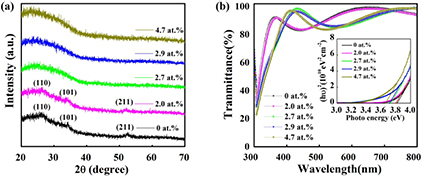
Figure 1. XRD patterns (a) and transmittance spectra (b) of the TWO thin films with different W doping contents annealed in air at 300 °C for 1 h. The inset in (b) is the Tauc plot extracted from the transmittance spectra.
Download figure:
Standard image High-resolution imageFigure 2(a) shows the O 1s regions of XPS spectra of TWO thin films with different W doping contents. By Gaussian fitting, these O 1s peaks are divided into three peaks OL, OM, OH, which are centred at 530.5 eV, 531.8 eV and 532.7 eV, respectively [21]. The low-energy peaks (OL) arise from oxygen ions combined with Sn ions. The mid-binding energy (OM) is associated with oxygen ions in the oxygen-deficient region within the TWO thin films. The high-energy peaks (OH) are combined with the adsorption oxygen, including absorbed H2O,−CO3, or O2. The variation of area proportion ( ) of three energy peaks shows that the relative quantity of the three oxygen states is changing along with the W doping content. Although it cannot provide accurate values of various oxygen state concentrations, it provides a trend of various oxygen state changes through the change of each peak area. The calculated results of each peak area proportion are listed in table 1. As W doping content increases from 0 to 4.7 at%, the OM area proportion reduces from 51% to 37% while the OL area proportion increases from 28% to 53%, which reveals that W doping can effectively suppress the oxygen vacancies. It can be explained by the fact that W–O bonding strength (672 kJ mol−1) is much stronger than Sn–O bonding strength (531.8 kJ mol−1) [22]. During sputtering and annealing process, oxygen is more likely to be caught due to the existence of W atoms resulting to the less oxygen vacancies. It is known that oxygen vacancy makes an important contribution to the high carrier concentration. To a TFT, the carrier concentration is not the more the better. With an excess carrier concentration, TFT appears a relatively large off-current resulted in large power consumption and low contrast, which are undesirable. In order to obtain better performance, suppressing carrier concentration to the appropriate range is very important. Incorporating higher binding strength element is effective for the suppression of carrier concentration, such as Ga doped IZO TFT [2], W doped IZO TFT [9] (Ga–O 353.5 kJ mol−1, W–O 672 kJ mol−1, In–O 320.1 kJ mol−1 and Zn–O 159 kJ mol−1 [22]). The difference of electronegativity between W (1.47) and O (3.61) is larger than that of Sn (1.82) [23, 24] makes a similar contribution to the carrier suppress effect as the bonding strength. From the results it can be speculated that other metals with higher metal–oxide binding strength and lower electronegativity than that of Sn (Sn–O bonding strength 531.8 kJ mol−1, electronegativity 1.82) also have potential to become effective carrier suppressors, such as Ca (Ca–O 589.8 kJ mol−1, 1.03), Sc (Sc–O 681.6 kJ mol−1, 1.15), Ti (Ti–O 672.4 kJ mol−1, 1.28), Sr (Sr–O 549.5 kJ mol−1, 0.96), Y (Y–O 719.6 kJ mol−1, 1.12), Zr (Zr–O 776.1 kJ mol−1, 1.32), Nb (Nb–O 771.8 kJ mol−1, 1.41), Hf (Hf–O 801.7 kJ mol−1, 1.16), Ta (Ta–O 799.1 kJ mol−1, 1.34), which need to be experimental verified. Other than the decreasing oxygen vacancy, it is worth noting that, the OH peak area proportion also decreases as the W doping content increases from 0 to 4.7 at%, which suggests that W doping can effectively suppress the adsorption of oxygen and is useful to improve the ageing stability of the TFTs. W 4f XPS spectra are shown in figure 2(b). When W doping content is less than 2.0 at%, W 4f peaks of W Spectra are not obviously observed. When the doping content is more than 2.7 at%, the peaks of W6+ around 34.5 eV, 36.7 eV corresponding to the W 4f7/2, 4f5/2 respectively are observed [25]. Sn 3d XPS spectra are shown in figure 2(c). The Sn peaks can be divided into two peaks of Sn (I) from 486.3 eV to 486.6 eV, and Sn (II) from 487.0 eV to 488.8 eV, respectively [26]. The Sn (I) corresponds to SnO states which act as impurities in the SnO2 crystal lattice while the Sn (II) is associated with the SnO2 states. It can be seen that W doping obviously reduces SnO related impurity phase in the SnO2 matrix. The Sn 3d shifts towards lower binding energy as W doping content increases, which originates from the substitution of the Sn atom with a W atom in Sn–O–Sn bonding and the formation of Sn–O–W bonding. With the lower electronegativity (1.47) compared with Sn (1.82), the W atom has a weaker ability to attract electrons, resulting an asymmetric electron clouds in the Sn–O–W bonding. The electron density around Sn atom increases after W incorporation, leading to the lower binding energy of Sn 3d. The Sn 3d shift indicates that the binding energy of the valence-band maximum (VBM) is decreased, that is to say, the VBM at the surface of TWO increases. It shifts the Fermi level towards valence band maximum (VBM), corresponding to the increase of the work function of the TWO surface [27–29]. The decrease of the Fermi energy at the surface of TWO also confirms the decrease of the carrier concentration.
Table 1. The calculated results of each peak area proportion of O 1s spectra.
| Energy (eV) | 0 | 2.0 at% | 2.7 at% | 2.9 at% | 4.7 at% |
|---|---|---|---|---|---|
| 530.50 (OL) | 0.28 | 0.38 | 0.41 | 0.51 | 0.53 |
| 531.80 (OM) | 0.51 | 0.47 | 0.45 | 0.38 | 0.37 |
| 532.70 (OH) | 0.21 | 0.15 | 0.14 | 0.11 | 0.10 |
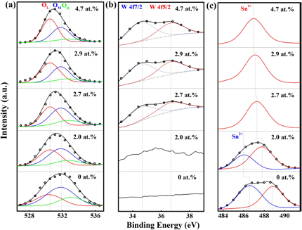
Figure 2. The O 1s (a), Sn 3d (b) and W 4f (c) of XPS spectra of TWO thin films with different W doping contents.
Download figure:
Standard image High-resolution imageFigure 3(a) shows the transfer curves of the TWO-TFTs with different W doping contents. All the TFT devices have the same channel layer thickness of 15 nm. Without doping W, the TFT shows a relative large off-current of 2.9 nA. As the W doping content increases to 4.7 at%, the off-current of TFTs decreases to 0.24 nA with the turn-on voltage VON (simply defined as VG at which ID starts to increase sharply in the log ID–VG curve) shifting rightward from −15.4 to 7 V, which can be explained by the fact that the channel carrier concentration is declined because of W acting as a carrier suppresser. With this rule, adjusting the TWO-TFT turn-on voltage is feasible, which can solve the problem that intrinsic SnO2 TFTs often show a depletion mode. It can be observed that W doping obviously reduces SS and increases on–off current ratio when W content is less than 2.7 at%, due to the decreased SnO related phase. But when W content is excessive, the W atoms not only act as oxygen vacancy suppressers but also form tungsten-related defects, which make SS increasing and mobility decreasing. There exists an optimum value of W doping content. Although the on-current also decreases in this case, the performance of TWO-TFTs is improved compared with intrinsic SnO2 TFTs. Figure 3(b) shows the main parameters of these TFTs with different W doping concentrations in which saturation mobility is calculated by the formula  where ID is the drain current, and VG the gate voltage, Ci (34.5 nF cm−2) the capacitance per unit area for the 100 nm thick SiO2 gate dielectric layer, W the channel width, L the channel length. The SS values are calculated by
  . From the figure it can be observed that the optimal performance is obtained at W doping content of 2.7 at%. The corresponding VON, saturation mobility, SS are 0.6 V, 4.6 cm2 V−1 s−1, 1.8 × 10⁶, 1.1 V/decade, respectively. Other than that, the channel layer is amorphous at W content 2.7 at%, which is important to ensure uniformity of the TFTs.
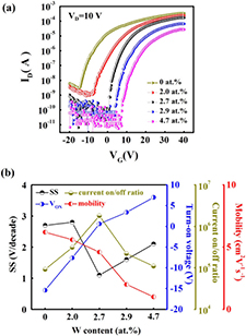
Figure 3. The transfer characteristic curves (a) and the main parameters (b) of the TWO-TFTs with different W doping contents.
Download figure:
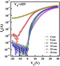
Standard image High-resolution imageFigure 4 shows the comparison of transfer curves of TFTs with different channel thicknesses. From the curves it can be observed that the thicker channel layer brings the problem to control the channel carrier concentration by the gate voltage, even though there is a larger on-state current. As the thickness is less than 15 nm, the drain current can be controlled well. As the channel layer continues to decrease, the VON stays at around 0 V while the SS value decreases first and then increases. Compared with the 15 nm thick channel TWO-TFT, the performance of TFT with 12 nm thick channel layer gets a promotion with a decreasing SS value to 0.4 V/decade, a lager on–off current ratio of 2.4 × 10⁶, an improved VON of 0.4 V and a slightly increased saturation mobility of 5 cm2 V−1 s−1. An excessively thin channel layer can cause the moisture in air easier to spread to the interface between the channel layer and the dielectric layer and makes the reaction with air ambient more serious. Such moisture related oxide performance degradation has been observed in the thin film technology [30]. It is believed that nanoporosity in dielectric thin film can facilitate H2O absorption to enable bond rupture, charged hydroxyl formation and defect creation, which results in the deterioration of SS values. Therefore, we obtain the optimal TFT performance with a channel thickness of 12 nm.
Figure 4. The transfer characteristic curves of the TWO-TFTs with different TWO channel thicknesses.
Download figure:
Standard image High-resolution image
Conclusions
We fabricated bottom gate thin film transistors with tungsten doped tin oxide as the channel layer. The TWO-TFTs show lower off-current and adjustable VON, which proves that W doping is conducive to suppress the carrier concentration of TWO channel layers. As the W content increases, the main TFT parameters SS value, VON and on–off current ratio become better then worse. The optimum TWO-TFT performance is obtained at W doping content of 2.7 at%. Reducing the channel layer thickness can improve the performance, the optimized channel thickness is 12 nm and the corresponding saturation mobility, turn-on voltage, subthreshold swing value and on–off current ratio are 5 cm2 V−1 s−1, 0.4 V, 0.4 V/decade and 2.4 × 10⁶. At the same time, the TWO channel layer is amorphous and the TFT works at enhancement mode. Thus, tungsten may be a promising dopant to improve the performance of the SnO2-based TFTs.
Acknowledgments
This work was supported by 973 Programme (2013CB328803) and the National Natural Science Foundation of China under Grant No 61136004, No 61471126.