

Abstract
The light-mater interaction in quantum dots doped artificial electromagnetic materials such as metamaterial waveguides has been studied. The effect of surface plasmon polaritons (SPPs) on the absorption coefficient of quantum dots in metamaterial waveguides is investigated. The waveguides are made by sandwiching a metamaterial slab between two dielectric material layers. An ensemble of quantum dots are deposited near the waveguide interfaces. The transfer matrix method is used to calculate the SSPs in the waveguide and the density matrix method and Schrödinger equation method are used to calculate the absorption spectrum. It is found that when the thickness of the metamaterial slab is greater than the SPP wavelength the SPP energy is degenerate. However when the thickness of the slab is smaller than that of the SPP wavelength the degeneracy of SPP state splits into odd and even SPP modes due the surface mode interaction (SMI) of the waveguide. We also found that the absorption spectrum has a minima (transparent state) which is due to strong coupling between excitons in quantum dots and SPPs in the waveguide. This transparent state is called the SPP induced transparency. However when the thickness of the slab is smaller than that of the SPP wavelength one transparent state in the absorption spectrum split into two transparent states due to the surface mode interaction. This type of transparency is called the SMI induced transparency. Transparent states can be achieved by applying pulse stress field or an intense laser pulse field. Hence present findings can be used to fabricate the metamaterial optical sensors and switches.
Export citation and abstract BibTeX RIS
1. Introduction
There is considerable interest in the study of the physical properties of artificial materials [1–8]. The first artificial materials were proposed by an Indian scientist, Bose, who studied the rotation of the plane of polarization by human-made twisted structures. These structures are artificial chiral structures by today's definition [1]. Later Lindell et al studied artificial chiral media formed by a collection of randomly oriented small wire helices [2]. Veselago [3] theoretically studied the uniform plane-wave propagation in an artificial materials which have both real negative permittivity and permeability values. He found that the direction of the Poynting vector of a monochromatic plane wave is opposite to that of its phase velocity. These materials are known as metamaterials. Smith et al [4] based on the work of Pendry et al [5] constructed a metamaterial in the microwave regime by arranging periodic arrays of the split-ring resonator (SRR) and metallic rod (MR) lattice. They found that these materials show the anomalous refraction at their boundaries that is the result of negative refraction. Since then, negative refraction has subsequently been realized in THz waves and at optical wavelengths [6–8]. The fabrication of metamaterials that will operate at optical wavelengths is an important research area [8, 9].
With numerous applications to nanophotonics optical waveguides play an important role in many fundamental studies of optical physics at nanoscale. Therefore, in order to obtain novel optical properties beyond the conventional dielectric waveguides, optical waveguides based on metamaterials have been studied [10–19]. Huang et al [11] studied wave propagation in nanowire waveguides made from extremely anisotropic metamaterials. They found that at a critical radius, the waveguide supports degenerate forward- and backward-wave modes with zero group velocity. He et al [12] propose nanoscale metamaterial optical waveguides with ultrahigh refractive indices based on metal–dielectric multilayer indefinite metamaterials with ultrahigh effective refractive indices. They found that waveguide modes depend on the cross sectional area of the waveguide.
Yao et al [14] found enhanced Purcell factors and Lamb shifts in the far-field emission spectra for a system containing a quantum dots near the surface of metamaterial waveguides. Metamaterial have also been used to fabricate a half-mode integrated waveguide [15]. It is found that they support the backward-wave propagation below the characteristic waveguide cutoff frequency in the left-handed region and the forward-wave propagation in the right-handed region [15]. Nanostructure metamaterial waveguides with hyperbolic dispersion have been shown to have significant effect on the photonic density of states [16]. Metamaterials are used as cladding in cylindrical waveguides doped with three-level atoms [17]. It is found the slowing of light and also decreased inherent loss [17]. Other novel optical properties of metamaterial waveguides such as slow-light propagation, subwavelength mode compression and surface mode guidance have also been studied [18, 19].
Some theoretical and experimental work has been done on the electromagnetically induced transparency in metamaterials. For example Zhang et al [20] have theoretically studied a plasmonic molecule consisting of a radiative element coupled with a subradiant (dark) element. Their theory relies on destructive interference between a bright dipole mode and a dark quadrupole mode in artificially designed plasmonic molecule. They suggested that molecules can be used as a building block to construct a plasmonic metamaterial. Liu et al [21] have investigated experimentally a nanoplasmonic analogue of the induced transparency using a stacked optical metamaterial. In their experiments a dipole antenna with a large radiatively broadened linewidth is coupled to an underlying quadrupole antenna with the narrow linewidth. They have achieved a very narrow transparency window in their experiment. Finally Weise et al [22] have studied hybridization induced transparency theoretically using an analytic model in a composite structure consisting of split ring resonators (SRRs) and α–lactose monohydrate. In their proof-of-principle experiment, induced transparency is observed due to the coherent coupling of a broadband mode of the SRRs to a narrowband mode resonance of α-lactose.
In this paper we study the light-matter interaction in hybrid materials which are made from quantum dots (QDs) and artificial electromagnetic materials such as metamaterial waveguides. The attraction of combining QDs and metamaterial waveguide stems from their complementary optical properties, which are long-lived excitations in QDs and localized electromagnetic modes (i.e. surface plasmon polaritons (SPPs)). The former gives rise to high emission yields and light-harvesting capabilities, while the latter enables the concentration of electromagnetic energy, enhanced optical fields and nonlinearities. Therefore, the combination of the two material systems can provide attractive opportunities to modify/design specific optical properties and to observe new phenomena that are based on exciton-SPP interactions. Besides a fundamental interest in the properties of exciton-SPPs, these hybrid materials have also attracted attention for their potential use in applications including optical sensing and switching devices for quantum information and communication applications.
The waveguide is made by sandwiching a metamaterial slab between dielectric material layers. A schematic diagram of the waveguide is shown in figure 1(a). Using the transfer matrix method the dispersion relation and density of states of SPPs for the waveguide are calculated for light with the transverse magnetic (TM) and the transverse electric (TE) modes. It is found that when the thickness of the metamaterial slab is greater than the wavelength of the SPP then both interfaces have degenerate SPP energy. However when the thickness of the slab is smaller than that of SPP wavelength the degenerate state splits into even-SPP and odd-SPP modes due the surface mode interaction (SMI) between two interfaces. QDs are doped at the interfaces of the metamaterials waveguide. Excitons of the QD interact with SPPs of the waveguide which is acting as reservoir. A probe laser field is applied to monitor the absorption coefficient and the density matrix method and Schrodinger equation method are used to calculate the absorption coefficient in the QDs.
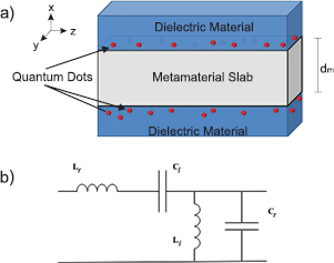
Figure 1. (a) A Waveguide made up of a metamaterial embedded within two dielectrics, doped with QDs near the interface. The Lattice constant is represented by am and the thickness of the metamaterial denoted by dm. (b) The unit cell can be represented by a circuit diagram composed of inductors and capacitors [21, 24].
Download figure:
Standard image High-resolution imageIt is found that when the thickness of the waveguide is larger than the wavelength of the light the system has one transparent state. We call it as the SPP induced transparency. However when the thickness of the slab is smaller than that of wavelength of the SPP the transparent state split into two transparent states due to the SMI. This is called the SMI induced transparency. Which means we have found that the system can be switched from an absorption state to a transparent state and also from one transparent state to two transparent states. These are very interesting findings of the paper and can be used to develop new types of optical switches from hybrid systems made from artificial electromagnetic materials. Switching can be achieved by applying pulse stress field or applying an intense pulse laser field.
2. Surface plasmon polaritons in metamaterial waveguides
The metamaterial waveguide is fabricated by sandwiching a metamaterial plate between two dielectric material layers. The thickness of the metamaterial layer is taken as dm. In the waveguide both materials lie in y–z plane and the y and z direction are taken to be symmetric. The first and second interfaces between the metamaterial and the dielectric lie at x = 0 and x = dm, respectively. A schematic diagram for the metamaterial waveguide is shown in figure 1(a). In general metamaterials are defined as artificial, effectively homogeneous, electromagnetic (EM) structures with unusual properties which are not found in natural materials. They have homogeneous structures and their unit cell am is much smaller than the wavelength λm of the EM wave propagating in the metamaterial. In other words the typical average size of the unit cell is am < λm/4 [23]. This condition is a long wavelength limit and can expressed as kmam < 1 where km is the Bloch wave vector of the EM wave and it is defined as km = 2π/λm. The different types of metamaterials are discussed in [23–25]. Metamaterials are fabricated by several groups by using a planar transmission line structures which are consists of a series of interdigital capacitors and shunt stub inductors [26, 27]. The unit cell of metamaterials can be expressed in terms of inductors and capacitors as shown in figure 1(b) [26, 27]. It has been proven in [26] that the dispersion relation of photons in most metamaterials are almost identical with very minor difference. Both metamaterials have energy gaps in their dispersion relation. The advantage of using metamaterials is that their photonic spectrum can be manipulated by the proper choice of capacitances and inductances of the right and left handed units.
Waveguide modes exist near the metamaterials interfaces and they are called SPPs. The dispersion relation for the metamaterial and the dielectric material is calculated as
where km is the Bloch wave vector of photons in metamaterial and kd is wave vector of photon in the dielectric. Here CR and LR are the capacitance and inductance of right handed part of the transmission line while CL and LL correspond to the left handed part of the transmission line. The am is the periodicity of the metamaterial. With the help of the unit cell given in figure 1(c), equation (1a) is calculated by using the transmission line theory [23–26].
To find SPPs in the metamaterial waveguide one has to consider that light decays near both interfaces along x direction in the metamaterial and in the dielectric material and the SPP wave travels along the y–z plane with wave vectors β. The x-component of wave vectors km and kd in the metamaterial and dielectric are denoted as κmx and κdx, respectively. Now we calculate the SPP modes TM and TE modes. We consider that in the TM mode magnetic component of the EM wave lies perpendicular to the y–z plane. Following the method [24, 27–29] and using the boundary conditions at x = 0 and x = dm for the waveguide we get a dispersion relation for the TM mode as


where  m = CR(1 − ℏ2/[CRLLε2])/(amε0) which is calculated in [23]. In the TE mode the electric component of the EM wave lies perpendicular to the y–z plane and we get a dispersion relation for the TM mode as
where μm = LR(1 − ℏ2/[CLLRε2])/(amε0) which is calculated in [23]. Note that equations (2) and (3) are function of κmx which is calculated numerically by solving equations (2) and (3) self consistently with the help of the MAPLE software package. Equations (2a) and (3a) give even-SPP modes denoted as κmx= while equations (2b) and (3b) give odd-SPP modes denoted as κmx=
 . The dispersion relation for the waveguide can be obtained by substituting
  in into equation (1a)

It is interesting to note that from the above expression the waveguide has two types of SPPs, called the even (+) and odd (−) SPP modes. It is found that equation (4) has singularities at certain values of energies say  . These energies
  and
and  are called SPP resonance states for each of the even and odd modes respectively.
3. Absorption coefficient and interaction Hamiltonian
An ensemble of noninteracting QDs are deposited near both interfaces of the waveguide. In this section we calculate the effect of the SPPs on the absorption coefficient of the QDs. We consider a QD that has three excitonic states denoted as ∣ a〉, ∣ b〉 and ∣ c〉 where ∣ a〉 is the excited state and ∣ b〉 and ∣ c〉 are two ground state (see figure 2). This type of systems have been studied by several groups [30, 31]. A probe field with energy εp and an amplitude Ep is applied to monitor the absorption coefficient for the transition ∣ a〉 ↔ ∣ b〉. The absorption coefficient due to absorption of a photon for the transition ∣ a〉 ↔ ∣ b〉 calculated in the literature [32] is written as

where ρab is the density matrix element and dab is the dipole moment induced in the QD due to the transition ∣ a〉 ↔ ∣ b〉. The density matrix ρab will be evaluated by using the density matrix method.
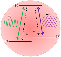
Figure 2. A three level lambda QD indicated ∣ a〉, ∣ b〉 and ∣ c〉 where ∣ a〉 is the excited state and ∣ b〉 and ∣ c〉 are two ground state. The energies of these states are εa, εb and εc, while γb and γc are the radiative linewidths of level ∣ b〉 and ∣ c〉, respectively.
Download figure:
Standard image High-resolution imageWe consider that the exciton due to the transition ∣ a〉 → ∣ c〉 and energy εac interacts with SPPs. One can also say that the metamaterial waveguide is acting as reservoir for the εac-exciton. The total Hamiltonian of the QD and metamaterial waveguide is written as

where gac is coupling constant of the εac-exciton-SPP interaction,

where dac is induced dipole moment due to the transition ∣ a〉 → ∣ c〉 and  is called the exciton raising operator for transition ∣ a〉 ↔ ∣ c〉. Operator
  is the SPP annihilation operator for energy
  and Vm is the volume of the metamaterial layer. Here
  and εi with i = a, b and c, are called the exciton number operator and energy level. The energy differences for ∣ a〉 ↔ ∣ b〉 and ∣ a〉 ↔ ∣ c〉 are denoted as εab = εb − εa and εac = εa − εc, respectively. Operator
  is the exciton raising operator and ap is the probe field photon annihilation operator. Here Ωp = dabEp/ℏ is the Rabi frequency associated with the probe field [33]. Here h.c. stands for the Hermitian conjugate. The first and second terms in equation (6) are the QD Hamiltonian and the interaction Hamiltonian between QD and the probe laser field due to transition ∣ a〉 → ∣ b〉, respectively. The third term in equation (6) is coupling of the εac-exciton and SPPs in the wave guide. This interaction is called the exciton-SPP interaction.
4. Density matrix method
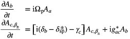
In this section we calculate the density matrix ρab appearing in equation (5). Using equation (6) and following the method of [23, 24, 34] we found the following density matrix equation for the QD and metamaterial waveguide system.
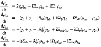
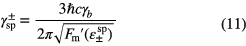
where δab = εp − εab is the probe detuning and  is called the SPP detuning. Here γb and γc are the radiative linewidths of levels ∣ b〉 and ∣ c〉, respectively. The function Ξac appearing in equation (8) is called the self energy due to εac-exciton and SPP coupling and is found as


where  the density of states (DOS) and expressions for β± is given in equation (4). The expression of Ξac can be simplified after some mathematical manipulations as

where  is the coupling constant and is written as
Here  is the derivative with respect to energy of equation (1a).
5. Results and discussions
In this section we have performed numerical simulations of bound SPPs, the density of states and the absorption coefficient. We have considered the dielectric materials in the waveguide as polyethylene. The material constants for the polyethylene are μd = 1 and d = 2.25 [35]. For the metamaterial we choose capacitances and inductances of the right- and left-handed components to be CR = 664 zF, LR = 57 fH, CL = 111 aF, LL = 51 fH. The periodicity of metamaterial is taken as am = 40 nm. These similar types of parameters are used in the literature for metamaterials [36]. In the present calculations we have chosen metamaterial parameters in such a range where SPPs energies lie in the visible light range. However, we can also design metamaterial waveguides to operate in the TeraHertz (THz) range by properly choosing the above physical parameters. Metamaterials in THz range have already been fabricated in the literature [25, 27]. Calculations presented in this paper are also valid for metamaterials with THz energies.
The SPP dispersion relation for the metamaterial waveguide has been calculated for TM and TE modes in figure 3. In the figure the energy and wave vector are normalized with the plasmon energy  [23] and plasmon wave vector kp = εp/ℏ c. The value of the plasmon energy is calculated as 8.0 eV. The normalized energy (ε/εp) is plotted as a function of the normalized wave vector (km/kp) for TM and TE modes in figures 3(a) and (b), respectively. In both figures the dotted and dashed curves correspond to dm = 10 µm and dm = 0.4 µm, respectively. We have chosen these numbers for dm so that dm = 0.4 µm satisfies the condition dm ≪ λspp/2π and dm = 10 µm satisfies the condition dm ≫ λspp/2π. Here λspp is the SPP wavelength.

Figure 3. The dispersion relation for the (a) TM and (b) TE modes of the metamaterial waveguide. Dotted curves corresponds to metamaterial where dm = 10 µm and dashed curves to dm = 0.4 µm. The positive signed curves represent the even TM and TE modes, while the negative signed curves represent the odd modes.
Download figure:
Standard image High-resolution imageFor the case dm ≫ λspp/2π (10 µm) in figure 3(a) we found two branches of dispersion relations for the TM mode and they are denoted as TM1 and TM2 (see two dotted lines). Each branch has one SPP resonance energy (εsp) and they are calculated as εsp = εTM1 = 0.371εp and εsp = εTM2 = 0.603εp. Similarly for dm ≫ λspp/2π in figure 3(b) the TE mode has two branches and they are denoted as TE1 and TE2. The SPP resonance energy for each branch is found as εsp = εTE1 = 0.150εp and εsp = εTE2 = 0.212εp.
SPPs experimentally and theoretically have also been studies by several groups in metamaterials heterostructures [23, 27, 32, 37]. Similar type of results are reported in these papers. However, it is worth pointing out that metal-dielectric heterostructurs have one SPP branch for the TE mode but there are no SPP branches for TE mode [25, 38].
For the case dm ≪ λspp/2π in figures 3(a) and (b) each SPP branch (dotted line) splits into even (+) and odd (−) branches (see dash curves in the both figures). This means that for dm ≫ λspp/2π SPP energies were degenerate and for dm ≪ λspp/2π case the degeneracy of the SPP energies is removed and it splits into even-SPP energy  and odd-SPP energy
  . The reason for splitting is the SMI between two interfaces of the waveguide.
The even-SPP and odd-SPP energies are calculated for TM1, TM2, TE1 and TE2 modes. It is found that for TM1 mode SPP energy εTM1 splits into  and
and  and for TM2 mode SPP energy εTM2 splits into
  and
and  . Similarly for the TE1 mode SPP energy εTE1 splits into
  and
and  and for the TE2 mode SPP energy εTE2 splits into
  and
and  .
.
The above results are supported by the findings of Hon et al [39] who studied terahertz metamaterial waveguides. They found the transmitted TM mode EM field decays exponentially away from the interface. This is signature of the bound SPPs in the waveguide. Solymar and Shamonia [27] have also shown splitting of SPPs due to the thickness of the metamaterials waveguides.
We now study the coupling of QDs with the SPPs of the metamaterials waveguide. To couple excitations of a QD to SPPs in our metamaterial waveguide we need two types of QDs, one to investigate the TM mode and another for the TE mode, since SPP energies have different values. For the first QD the resonance energy is given as εac = 0.370εp which lies very close to SPP energy for the TM1 mode εTM1 = 0.371εp. Similarly for the second QD the resonance energy is given as εac = 0.215εp which lies near to SPP energy for the TE2 mode εTE2 = 0.212εp. This type of QDs has been recently fabricated [39]. Other parameters for the first QDs are the dipole moments, dac = 4.8 · 10−28 Cm, the linewidth of level ∣ b〉, γb = 32 meV and the linewidth of the level ∣ c〉, γc = 10−5 meV. Similarly for the second QD other parameters are taken as dac = 8 · 10−28 Cm, γb = 64 meV and γc = 10−5 meV.
Let us investigate the effect of the exciton-SPPs coupling on the absorption coefficient. First we consider the case dm ≫ λspp/2π (i.e. dm = 10 µm). Here we have focused our investigation to the lower energy region of the TM1 mode (εTM1) and the upper energy region of the TE2 mode (εTE2). We have chosen these modes because their energies are close to the QD resonance energy εac as discussed in the previous section.
In figures 4(a) and (b) the absorption coefficient is plotted as a function of probe detuning δab for the TM and TE modes, respectively. The solid lines correspond to dm = 10 µm when the SPP frequencies εTM1 and εTE2 are not resonance with QD energy εac. Here we have taken δsp = εac − εTM1 = 0.00138εp and δsp = εac − εTE2 = 0.00288εp for both modes. Note that δsp = 0 corresponds to resonance condition. The solid line in both figures has one peak at δab = 0. This peak is due to he absorption due to the transition ∣a〉 ↔ ∣b〉. Now consider the situation when the SPP frequencies εTM1 and εTE2 are resonant with QD energy εac i.e. δsp = 0. The results are plotted as the dotted line in both figures. Notice that in this case the absorption spectrum has two peaks and a minimum in both figures. The minimum appears at δab = δsp and it corresponds to a transparent state.
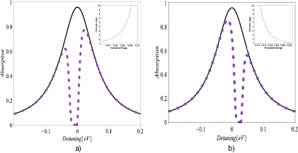
Figure 4. Plot of the absorption coefficient of the QD as a function of probe detuning for (a) TM and (b) TM modes of the metamaterial waveguides. Solid curve corresponds to the energies where SPP frequencies εTM1 and εTE2 are not resonant with QD energy εac. Dotted curve corresponds to the energies where SPP frequencies εTM1 and εTE2 are resonant with QD energy εac. For both figures dm = 10 µm. Inset: the DOS for the (a) TM and (b) TE SPPs.
Download figure:
Standard image High-resolution imageThe splitting of one peak to two peaks and appearance of the transparent state can be understood as follows. For dm ≫ λspp/2π the SPP energy is degenerate and hence the self energy becomes Ξac = 
 . The self energy depends on DOS (see equation (9a)) and it is plotted as function of normalized energy in insets of both figures 4(a) and (b). Note that the DOS for the TM1 mode has singularities near εsp = εTM1 = 0.371εp and the DOS for the TE2 mode has singularities near εTE2 = 0.212εp. This in turn enhances the self energy Ξac which is nothing but the εac-exciton-SPP interaction. Due to this strong interaction the excited state ∣a〉 splits into two dressed states ∣a1〉 and ∣a2〉 for both TM1 and TE2 waves. Hence two absorption peaks appear in the spectrum due to transitions ∣b〉 ↔ ∣a1〉 and ∣b〉 ↔ ∣a2〉 and a transparent state appears between two peaks. One can also say that the transparency occurs due to the match between the wave vector in the waveguide and the momentum required for the energy relaxation in the transition ∣a〉 ↔ ∣c〉. When this match is fulfilled, there will be no absorption and the transparent state appears.
We found that the transparency appears for dm ≫ λspp/2π in the system due to strong excition-SPP coupling. We call this phenomenon as the SPP induced transparency (SPPIT). The system can be switched from a absorbing state to a transparent state due to the exciton-SPP coupling. This can be achieved by modifying the SPPs energy by using an external stress or the external intense laser field. This in turn modifies the exciton-SPP coupling.
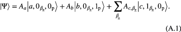
We investigate now the size effect of metamaterial slab on the absorption coefficient for TM1 and TE2 modes. We reduce the size of the waveguide such that we have the condition dm ≪ λspp/2π(dm = 0.4 µm). We consider that the TM1-SPP energy is in close resonance with QD energy (i.e. εac − εTM1 = 0.001 38εp) and the TM1-SPP energy is also in close resonance with QD energy (i.e. εac − εTE2 = 0.002 88εp). The numerical results are plotted in figures 5(a) and (b), for TM1 and TE2 modes, respectively. The dashed lines correspond to dm << λspp/2π and dotted lines represent dm ≫ λspp/2π, respectively in both figures. Note that the dotted line has one minimum which is located at δab = δsp as discussed in figure 4. On the other hand the dashed lines have three peaks and two minima which are located at  and
and  .
.

Figure 5. Plot of the absorption coefficient of the QD as a function of probe detuning for (a) TM and (b) TM modes of the metamaterial waveguides. Dotted curve corresponds to the energies where SPP frequencies εTM1 and εTE2 are resonant with QD energy εac, with dm = 10 µm. Dashed curve corresponds to the energies where SPP frequencies εTM1 and εTE2 are resonant with QD energy εac, dm = 0.4 µm. Inset: the DOS for the (a) TM and (b) TE SPPs.
Download figure:
Standard image High-resolution image
The origin of two minima can be understood as follows. Note that due to the SMI εTM1 splits into  and
and  and εTE2 splits into
  and
and  . The self energies
  and
and  for the even-SPP and odd-SPP modes have large values at
  and
and  , respectively due to the large DOS (see insets). The εac-exciton strongly couples with even-SPP (i.e.
  and odd-SPP
  and due these couplings the excited state ∣a〉 splits into three dressed states ∣a1〉 ∣a2〉 and ∣a3〉. Hence the absorption spectrum has three peaks due to transitions ∣b〉 ↔ ∣a1〉, ∣b〉 ↔ ∣a2〉 and ∣b〉 ↔ ∣a3〉 and two transparent states located at
  and
and  . One can also say that for one εac-exciton wave vector there are two even-SPP and odd-SPP energies. So there are two absorption dips (transparent states).
Here we found that the one transparent state splits into two transparent states by changing the thickness of the metamaterial slab. This splitting is nothing but due to the SMI between SPP located the two interfaces of metamaterial. This transparency can be called the SMI induced transparency (SMIIT).
The Schrödinger equation method of appendix has also been used for numerical calculations of absorption coefficient. This method gives the similar results as found in this paper.
6. Conclusion
In summary we have studied the optoelectronic properties of the QD and metamaterial waveguide. The SPP energies are found at two interfaces for the metamaterial waveguide. We found that when the thickness of the metamaterial slab is greater than the SPP energy is degenerate. Whereas when the thickness of the slab is smaller than that of SPP wavelength the degeneracy of the SPP energy is removed. The degenerate state splits into odd SPP modes and even SPP modes due the SMI between two interfaces. The absorption coefficient in QD has been calculated and it has been found that absorption spectrum has one minima when the thickness of the metamaterials slab is larger than the SPP wavelength. This minimum is due to the strong coupling between excitons in QD and SPP in waveguide. The minima is nothing but the transparent state in the system and it is called the SPP induced transparency (SPPIT). However when the thickness of the slab is smaller than that of SPP wavelength the transparent state splits into two transparent states due to the SMI. The two transparent states found within the system is called the SMI induced transparency (SMIIT). Transparent states can be achieved by applying stress field or applying an intense laser pulse field. Hence present findings can be used to fabricate the metamaterial optical switches. The Schrödinger equation method given in the appendix has also been used for numerical calculations and similar results are found.
Acknowledgments
M Singh is thankful to the Natural Science and Engineering Council (NSERC) of Canada for research funding.
Appendix A.: Schrödinger equation
In this appendix we derive the expression of the absorption coefficient using the Schrödinger equation method. We need to expand the wave function ∣Ψ〉 as an orthonormal set. To find the orthonormal set we consider that initially the electron in the QD is in the ground state ∣ b〉 and there is one probe photon present ∣ 1p〉. SPPs in the waveguide are in the ground state  . This initial state is denoted as
  . Therefore, we find the three orthonormal states of the system to be
  and
and  as the wave function as follows
Solving the Schrödinger equation with equation (A.1) we get
where δab = εp − εab is the probe detuning and γb and γc are the radiative linewidths of levels ∣ b〉 and ∣ c〉, respectively. The summation in equation (A.2) can be replaced by using the method of DOS as

where D± is defined in equation (9b). The expression of ρab appearing in equation (5) can be calculated from the expansion coefficients as  . Therefore ρab is calculated numerically by solving the three Schrödinger equations (A.2).
An analytical expression of ρab can also be found from equation (A.2) in the steady state as

where ρbb = ∣ Ab∣2 and  is found in equation (9a). The above expression can be used to calculate the absorption coefficient given in equation (5). One can see from the equation (A.4) that if we neglect the coupling the QD and SPPs we get
  and the absorption peak appears at δab = 0.