
Abstract
This paper reviews recent advances in graphene active plasmonics for terahertz (THz) device applications. Two-dimensional plasmons in graphene exhibit unique optoelectronic properties and mediate extraordinary light–matter interactions. It has been discovered theoretically that when the population of Dirac fermionic carriers in graphene are inverted by optical or electrical pumping, the excitation of graphene plasmons by the THz photons results in propagating surface plasmon polaritons with giant gain in a wide THz range. Furthermore, when graphene is patterned into a micro- or nanoribbon array by grating metallization, the structure acts as an active THz plasmonic amplifier, providing a superradiant plasmonic lasing with a giant gain at the plasmon modes in a wide THz frequency range. These new findings can lead to the creation of new types of plasmonic THz emitters and lasers operating even at room temperature.
Export citation and abstract BibTeX RIS
1. Introduction
Despite its tremendous application potential, the terahertz (THz) frequency range of the electromagnetic spectrum is not widely used in practice yet. This in part is because there are no commercially available microelectronic or nanoelectronic devices, which are able to generate, detect, or manipulate the THz electromagnetic waves. The creation of compact, efficient, room-temperature operating and tunable THz devices, particularly THz sources, is still a challenging task stimulating extensive research activity. Due to fundamental limits, the available THz sources utilizing the excitation of the classical electron oscillations with microwave and somewhat higher frequencies, as well as those based on electron transitions between quantized energy levels corresponding to infrared and optical frequencies are unable to cover the entire THz range. This results in the existence of the so-called terahertz gap [1, 2].
The quantum cascade laser (QCL) is one of the most developed compact solid-state sources in mid-infrared frequency range. In the last decade, significant progress in the development and applications of QCLs has been demonstrated. However, the THz-QCL radiation power steeply decreases with a decrease of the frequency down to 1 THz and with an increase of the operation temperature up to room temperature [3–6]. Moreover, THz QCLs still exhibit insufficient tunability and functionality associated with their fairly complex device structure (requiring state-of-the-art fabrication techniques), necessitating deep cooling or application of high magnetic fields. Optical heterodyne conversion, or photomixing, in semiconductors is an alternative technique generating THz radiation at room temperature utilizing low-temperature-grown GaAs (LT-GaAs) photoconductors (PCs) [7–9] and pin photodiodes (PDs) [10] as well as uni-travelling-carrier photodiodes (UTC PDs) [11]. So far, excellent performance of over 5 THz generation using LT-GaAs PCs [7] and over 10 µW emission power at 1.04 THz using UTC PDs [11] has been demonstrated. Their quantum efficiencies, however, are substantially limited by their two-terminal device structures, although new promising ideas including travelling-wave structures [8, 9] and/or ballistic transport structures [12] have emerged.
The utilization of new physical mechanisms and/or the extraordinary electronic and photonic properties of the nonstandard materials might promote bypassing the existing limits and bridge the terahertz Gap. Among such materials, graphene, a one-atom-thick planar sheet of sp2-hybridized honeycomb carbon crystal, has attracted considerable attention because of its unique carrier transport and optical properties [13–19]. The groundbreaking discovery of graphene triggered the research and development of graphene-based electronic, optoelectronic and THz photonic devices. Graphene channel transistors increase their cutoff frequencies approaching THz range [20–22], whereas graphene photodetectors demonstrate high-speed operation [23] in the mid-infrared range, being expected to operate also in THz range [24].
The conduction and valence bands of graphene have a symmetrical conical shape around the Brillouin zone edges, which are called K and K' points, and contact each other at 'Dirac points' at the K and K' points. Electrons and holes in graphene have a linear energy dispersion relation with zero bandgap, resulting in peculiar features such as massless relativistic fermions with back-scattering-free ultrafast transport [14–19, 25, 26] as well as negative dynamic conductivity at THz frequencies under optical or electrical pumping [27–34].
Two-dimensional (2D) plasmons in graphene exhibit unique optoelectronic properties and mediate extraordinary light–matter interactions. So far, 2D plasmons in graphene have been intensively studied theoretically [35–60], and very recently graphene plasmons have been experimentally observed [61–65]. When graphene is patterned into micro-/nanocavities, the frequencies of plasmon modes in these cavities fall into THz range. Terahertz plasmons in graphene can be excited via a stimulated emission process if the cavity boundary conditions allow the plasmon instability or the THz dynamic conductivity of graphene in the plasmon cavity becomes negative due to optical or electrical pumping [36, 39, 43, 47, 50, 54, 66]. In nanopatterned graphene, the plasmons strongly couple to THz electromagnetic radiation [61] which can give rise to stimulated THz emission. This paper reviews recent advances in graphene active plasmonics for stimulated emission of THz radiation.
2. Fundamentals of 2D plasmons in graphene
Collective excitation of 2D plasmons in graphene exhibits extraordinary THz properties, such as extremely high plasmonic absorption as well as a giant plasmonic gain at THz frequencies [17–19, 36, 39, 41, 43, 45, 47, 48, 50, 54, 55]. The dispersion of plasmons has been derived for ungated [35, 37, 38, 44, 45, 48, 52] and gated [36, 39, 43] graphene, gated pin graphene junctions [58], graphene ribbon arrays [40, 46, 56, 57], graphene edges [49, 52, 59], and for double- and multiple graphene structures [67–71]. In particular, the gated plasmons are of major practical interest for use in frequency-tuned device applications. The gated plasmons have a superlinear dispersion in which the gate-to-graphene distance d and the carrier momentum relaxation rate (collision frequency) deform the linear dispersion relations (figure 1(a)). The semi-classical Boltzmann equation can describe the electron–hole plasma-wave dynamics in graphene [36, 39, 53]. The plasmon phase velocity is proportional to the quarter power of the gate bias and of d [36, 39, 53] and always exceeds the Fermi velocity vF [36, 39], which is quite different from those for the 2D plasmons in conventional semiconductor quantum wells. Intrinsic graphene and/or phtoexcited graphene have equal densities of electrons and holes so that bipolar e–h modes of plasmons are excited in this case. As a result, two different branches of carrier waves: the plasma waves and charge-neutral sound-like waves can be excited (figure 1(b)). In undoped (ungated) graphene, the e–h plasmons are strongly damped whereas the e–h sound-like waves survive. On the other hand, doped (gated) graphene has large fraction on the majority and minority carriers. The plasma waves originating from the minority carriers are strongly damped, thus only unipolar plasmon modes of the majority carriers exist.
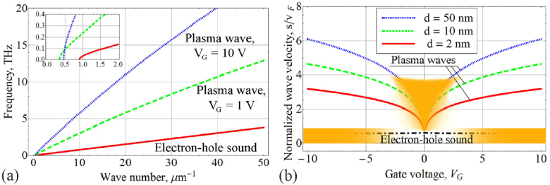
Figure 1. (a) Dispersion relation of gated graphene plasmons. (b) Plasma-wave velocity versus gate bias. Dashed–dotted line corresponds to the electron–hole sound-like waves in the vicinity of the neutrality point. Regions of strong damping are filled. The inset in (a) magnifies the small wave number range exhibiting the superlinear properties (after [57]).
Download figure:
Standard image High-resolution imageTerahertz plasmon modes in a graphene micro-ribbon array structure were experimentally observed to verify the theoretical dispersion relations [61–65]. Plasmon frequencies in graphene micro-arrays can be tuned through the entire THz range, depending on (i) the direction of the plasmon propagation in the array plane and/or (ii) the micro-ribbon width, (iii) electrostatic modulation of the carrier density and (iv) Landau-level splitting under magnetic field. Plasmons in patterned graphene are strongly coupled to electromagnetic waves, which constitutes a potential for development of tunable graphene-based THz plasmonic metamaterials [55, 61, 72, 73]. Therefore, the prospects of graphene plasmonics for mid-infrared and THz applications attract a rapidly growing interest [17–19, 48, 49].
A number of models of the graphene conductivity have been developed so far [60], each being valid in a certain range of frequencies and carrier densities. In high-frequency (from THz to infrared) range, the following relation for the graphene conductivity derived from the Kubo formula is valid [74],
where the indices 1 and 2 refer to conduction and valence bands, ε1 (p) = |p|vF and ε2(p) = −|p|vF,
 is the electron distribution function (the equilibrium Fermi function f(ε) = 1/[1 + e(ε−εF)/T] is assumed), vx = vF cos θp and v12 = ivF sin θp are the matrix elements of the velocity operator. The first term in equation (1) corresponds to the intraband transitions, whereas the second term corresponds to the interband transitions. To allow for the electron (hole) momentum relaxation, one should treat the frequency in the intraband part of the conductivity expression as
 . The definite expressions for different scattering processes can be found in [60]. For example, when electron–phonon scattering is the dominating mechanism, the corresponding relaxation time is given by the following formula [75]:

where the parameter
 at room temperature T ≃ 26 meV. Then the real part of equation (1) can be expressed in the following simple form [76–78]:
where e is the elementary charge, ℏ is the reduced Planck's constant,, kB the Boltzmann the constant, T is the temperature, and τm is the momentum relaxation time of carriers. The intraband contribution,
 , corresponds to the Drude absorption and is always positive. The THz frequency domain is situated in the intraband Drude conductivity dominated region. The dynamics of the plasma-waves is described by the hydrodynamic Euler equation and continuity equation derived from semi-classical Boltzmann equations for massless Dirac fermions. As is seen in figure 2, in a low frequency region including THz range, the intraband Drude conductivity is dominated and decreases with increasing frequency [78]. The intraband Drude conductivity can be modulated by doping- and structure-dependent plasmonic behaviours [78–80] as is done in normal semiconductor heterostructures [81]. The interband conductivity vanishes due to the Pauli blocking. At photon energy twice as large as the Fermi level, the interband conductivity starts to increase and saturates at a plateau of the quantum conductivity e2/4ℏ.

Figure 2. Frequency dependence of a real part of the optical conductivity of graphene. The dashed lines are with the Fermi level at 100 meV, whereas the solid lines are for higher doping with the Fermi level at 200 meV. With increasing doping, thus the carrier densities and resultant Fermi level, the intraband Drude conductivity increases and the roll-off frequency of the interband conductivity shifts up due to widening the Pauli-state blocking (after [78]).
Download figure:
Standard image High-resolution image3. Towards the creation of THz plasmonic lasers
3.1. Quantum limitation on THz stimulated photon emission
Interband population inversion in graphene can be achieved by its optical pumping [27, 29] or carrier injection [28, 29]. At sufficiently strong excitation, the interband stimulated emission of photons can prevail over the intraband (Drude) absorption. In this case, the real part of the dynamic conductivity of graphene, Re[σ(ω)], becomes negative at some frequencies ω. Due to the gapless energy spectrum of graphene, Re[σ(ω)] can be negative in THz range. This effect can be exploited in graphene-based THz lasers with optical or injection pumping. Graphene photonic lasers with the Fabry–Pérot resonators based on dielectric or slot-line waveguides [30] were proposed for lasing the THz photons. Stimulated emission of near-infrared [82] and THz [31, 32] photons from population-inverted graphene was observed experimentally.
It is worth noting that the negative THz conductivity of monolayer graphene is limited to the quantum conductivity (e2/4ℏ) as seen in equation (9). This is because the absorption of THz photons that can contribute to the stimulated emission is only made via interband transition process whose absorbance is limited by
 [83]. To overcome this limitation on quantum efficiency, a carrier recycling process like that exploited in QCLs can be introduced. In this regard, waveguide structures with in-plane THz photon propagation along the graphene sheet are preferable for comprising the laser cavities in order to maximize the gain overlapping and hence to overcome the quantum mechanical limit in comparison with vertical photon-emitting cavity structures [30]. However, even for 20-multiple-layered graphene that can increase the absorbance by almost 20 times, the absorption coefficient of THz photons along the inverted graphene is still relatively low, on the order of 1 cm−1 [30]. To overcome this quantum-conductance limit, introduction of surface plasmon polaritons (SPPs) is a promising and important idea. Due to its extremely slow-wave nature (three to four orders of magnitude lower than photon speed), effective interaction efficiency can be increased by three to four orders corresponding to the ratio of the speed of plasmons to that of the photons, resulting in orders of increase in gain coefficient. There are several factors to exploit the graphene plasmons: (i) the excitation and propagation of the SPPs along population-inverted graphene [39, 43, 47, 54], (ii) giant gain of SPPs due to their small group velocity and strong localization of SPP in the vicinity of graphene layer [43, 47], (iii) the resonant plasmon absorption in structured graphene like micro-ribbon arrays, microdisc arrays [61–65, 78, 84, 85] as well as double- and multiple graphene structures [67–71], and (iv) superradiant THz emission mediated by the SPPs [54, 66].
3.2. THz emission from electron–hole plasma originated from transient photocurrent
Plasmon emission due to recombination of the electron–hole pairs in graphene was demonstrated experimentally in [14, 86]. Prechtel et al observed time-resolved picosecond photocurrents in freely suspended graphene contacted by metal stripline electrodes [86] (figure 3). They spatially resolved picosecond photocurrents in the sample. Built-in electric fields at the graphene–metal interface give rise to a transient photocurrent with a full-width-half-maximum of ∼4 ps and then a slower decaying current with a decay time of ∼130 ps is generated due to a photothermoelectric effect. Furthermore, it has been shown that, in optically pumped graphene, electromagnetic radiation up to 1 THz is generated. The authors interpret these oscillations with Fourier-transformed amplitudes up to 1 THz as originated from THz radiation emitted from electron–hole plasma in the optically pumped graphene. These results may prove essential to building graphene-based plasmonic terahertz emitters.

Figure 3. Terahertz generation in suspended graphene by transient photoconductive currents. (a) Freely suspended graphene incorporated into a coplanar stripline circuit, and spatially resolved scan of incident photocurrent Iphoto. The position of the striplines is indicated with dashed lines. Single line-sweep of Iphoto along the dotted line is also plotted. (b) Measured photoconductive current Isampling for excitation positions starting at the graphene–metal interface in steps of 2 µm (from bottom to top) along the dotted line in (a). (c) Upper panel: the lowest trace in (b) but extended up to 180 ps time delay with its fitting function. Lower panel: the individual components extracted from the trace in the upper panel: the transient displacement current (dotted line) and the photothermoelectric current (dashed line). (d) Built-in electric-field at the metal–graphene interface generates transient photocurrent due to weak symmetry breaking and e–h plasmon excitations at 77 K (left) and corresponding fast-Fourier-transformation of interpolated Isampling (right). The data offset level is indicated with dashed lines (after [86]).
Download figure:
Standard image High-resolution image3.3. THz giant gain by excitation of SPPs in inverted graphene
As compared with the THz lasing due to the stimulated emission of the electromagnetic modes (i.e., photons), the stimulated emission of plasmons by the interband transitions in population-inverted graphene can be a much stronger emission process. The plasmon gain under population inversion in intrinsic graphene has been theoretically studied in [47, 54]. Non-equilibrium plasmons in graphene can be coupled to the TM modes of electromagnetic waves when pertinent structures and/or spatial charge-density distributions are arranged to excite the SPPs [87–89], resulting in formation and propagation of SPPs [47]. It is shown in [47] that the plasmon gain in pumped graphene can be very high due to small group velocity of the plasmons in graphene and strong confinement of the plasmon field in the vicinity the graphene layer, figure 4 (left). The propagation index ρ of the graphene SPP along the z coordinate is derived from Maxwell's equations:

where n is the refractive index of the substrate, c is the speed of light in vacuum, and σω is the conductivity of graphene at frequency ω [47]. When n = 1, ρ becomes
The absorption coefficient α is obtained as the imaginary part of the wave vector along the z coordinate: α = Im(qz) = 2Im(ρ · ω/c). Figure 4(right) plots simulated α for monolayer graphene on a dielectric substrate with various refraction indices at 300 K. To drive graphene in the population inversion with a negative dynamic conductivity, a quasi-Fermi energy εF = 20 meV and a carrier momentum relaxation time τ = 10 ps are assumed, respectively. The results demonstrate giant THz gain (negative values of absorption) on the order of 104 cm−1. This giant gain comes from the slow-wave nature of the SPPs as mentioned in section 3.1. An increase in the substrate refractive index and, consequently, stronger localization of the surface plasmon electric and magnetic fields, results in markedly larger gain, i.e. negatively larger absorption coefficient (compare curves 1 and 2 in figure 4). Comparison of curves 2 and 3 in figure 4 shows that the contribution of the substrate loss to the surface plasmon absorption can be relatively weak at realistic values of the imaginary part of the substrate refractive index (corresponding to curve 3). In particular, in the case of the substrate of undoped Si (Im(n) ∼ 3 × 10⁻⁴), the imaginary part of the refractive index can be smaller than those used in the calculations of curves 3–5 in figure 4. Waveguiding the THz emitted waves with less attenuation is another key issue to create a graphene THz laser.
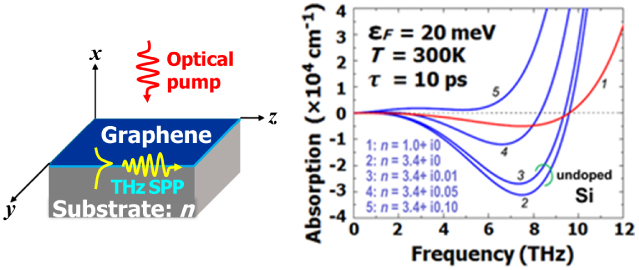
Figure 4. Frequency dependences of SPP absorption for monolayer population-inverted graphene for different substrate refraction indices n (1: n = 1.0, 2: n = 3.4, 3: n = 3.4 + i0.01, 4: n = 3.4 + i0.05, and 5: n = 3.4 + i0.1) at 300 K for the quasi-Fermi energy εF = 20 meV and carrier momentum relaxation time τ = 10 ps. The results demonstrate giant THz gain (negative values of absorption) of the order of 104 cm−1 (after [47]).
Download figure:
Standard image High-resolution imageIt is also important to consider the spatial dispersion of the SPPs [90], i.e., the dependence of σω on SP wave number qz in equation (3) [47, 71]. When ρ < c/vF or ω < Re(qz)vF the spatial dispersion is negligible [42]. As shown in figure 5, when n = 1 this condition is preserved in the THz frequency range under consideration. However, when n = 3.4 of a realistic case it is limited to relatively low THz frequencies (ω/2π ⩽ 5–8 THz); SPs becomes spatially dispersive at frequencies ω/2π ⩾ 5–8 THz. Recent study reveals that such spatial dispersion of conductivity significantly augments the free path and cutoff frequency of SPPs [71], which could be of great importance for practical THz device applications.

Figure 5. Frequency dependences of the real part of the propagation index Re(ρ) (solid lines) and the SP group velocity normalized to the speed of light (dotted lines) for monolayer graphene structure with different substrate refractive index (n = 1.0 (a) and 3.4 (b)) at T = 300 K and different quasi-Fermi energies (1:εF = 0 meV, 2:εF = 10 meV, 3:εF = 20 meV). When Re(ρ) > c/vF the SP becomes spatially dispersive (after [47]).
Download figure:
Standard image High-resolution image3.4. Superradiant THz plasmon emission from inverted graphene–metal micro-ribbon arrays
The amplification of THz waves by stimulated generation of resonant plasmons in a planar periodic array of graphene plasmonic microcavities has been theoretically studied using a self-consistent electromagnetic approach in [54]. Figure 6(a) depicts the graphene device structure. Graphene microcavities are confined between the metal grating contacts located on a flat surface of a dielectric (which can be Si or SiC in a practical case) substrate. External THz wave is incident upon the planar array of graphene microcavities at normal direction to its plane with the polarization of the electric field across the metal grating contacts. Suppose that the graphene is pumped either by its optical illumination [27, 30, 32] or by injection of electrons and holes from opposite metal contacts in each graphene microcavity [28, 29]. In the latter case, the opposite ends of each graphene microcavity adjacent to the metal contacts have to be p- and n-doped [28, 29]. One can easily imagine a biasing scheme for applying dc voltages to successive metal contacts in an interdigital manner [87] in order to ensure injection of the carriers into each graphene microcavity. The carrier population and hence the dynamic conductivity are characterized by the quasi-Fermi level and carrier temperature as described in equation (3).

Figure 6. (a) Schematic view of the array of graphene micro-/nanocavities. The incoming electromagnetic wave is incident from the top at normal direction to the structure plane with the polarization of the electric field across the metal grating contacts. The energy band structure of pumped graphene is shown schematically in the inset. (b) Contour map of the absorbance as a function of the quasi-Fermi energy and the frequency of incoming THz wave for the array of graphene microcavities with period L = 4 µm, the length of each graphene microcavity a = 2 µm, and the electron scattering time in graphene τ = 10−12 s. Blue and red arrows mark the quasi-Fermi energies for the maximal absorption and for the plasmonic lasing regime, respectively, at the fundamental plasmon resonance. (c) The variation of the power amplification coefficient along the first-plasmon-resonance lobe. (d) Schematic illustration of the energy rate balance in the plasmon lasing regime. (e) Distribution of the normalized induced in-plane electric field at the moment of time corresponding to the maximal swing of plasma oscillations in the graphene microcavities at the fundamental plasmon amplification resonance (after [54]).
Download figure:
Standard image High-resolution image
Figure 6(b) shows the contour map of the calculated absorbance as a function of the quasi-Fermi energy (which corresponds to the pumping strength) and the THz wave frequency for an array of the graphene microcavities with period L = 4 µm and the length of each microcavity a = 2 µm. In the amplification regime, the negative value of the absorbance yields the amplification coefficient. The value of Re[σGr (ω)] is negative above the solid black line in figure 6(b), corresponding to Re[σGr(ω)] = 0 (i.e., to transparent graphene). Above this boundary line, negative absorption (i.e., amplification) takes place at all frequencies and pumping strengths. The plasmon absorption resonances below the Re[σGr(ω)] = 0 line give way to the amplification resonances above this line. Plasmon resonances appear at frequencies ω = ωp(q) determined by the selection rule for the plasmon wave vector qn = (2n − 1)π/aeff, where aeff is the effective length of the graphene micro-/nanocavity. The frequency of the plasmon resonance is determined mainly by the imaginary part of the graphene conductivity, while the real part of the conductivity (3) is responsible for the energy loss (for Re[σGr(ω)] > 0) or energy gain (for Re[σGr(ω)] < 0).
With increasing εF, the energy gain can balance the energy loss caused by the electron and hole scattering in graphene so that the net energy loss becomes zero, Re[σ(ω)] = 0, which corresponds to graphene transparency. In this case, the plasmon resonance line exhibits a non-symmetric Fano-like shape because the real part of graphene conductivity changes its sign across the plasmon resonance. In this case, the plasmon resonance linewidth is given solely by its radiative broadening (because the dissipative damping is close to zero in this case). Above the graphene transparency line Re[σGr(ω)] = 0, the THz wave amplification at the plasmon resonance frequency is several orders of magnitude stronger than away from the resonances (the latter corresponding to the photon amplification in population-inverted graphene [27–34]). Note that at a certain value of the quasi-Fermi energy, the amplification coefficient at the plasmon resonance tends towards infinity with corresponding amplification linewidth shrinking down to zero. Unphysical divergence of the amplification coefficient is a consequence of the linear electromagnetic approach used in [54]. This corresponds to plasmonic lasing in the graphene micro-/nanocavities in the self-excitation regime. The behaviour of the amplification coefficient around the self-excitation regime is shown in figure 6(c). The lasing occurs when the plasmon gain balances the electron scattering loss and the radiative loss, see figure 6(d). It means that the plasmon oscillations are highly coherent in this case, with virtually no dephasing at all. The quasi-Fermi energy corresponding to plasmonic lasing in the first plasmon resonance is marked by the red arrow in figure 6(b).
It is worth noting that the plasmons in different graphene microcavities oscillate in phase (even without the incoming electromagnetic wave) because the metal contacts act as synchronizing elements between adjacent graphene microcavities. The plasmon-mode locking regime in different graphene nanocavities is shown in figure 6(e). Therefore, the plasma oscillations in the array of graphene microcavities constitute a single collective plasmon mode distributed over the entire area of the array, which leads to the enhanced superradiant electromagnetic emission from the array. Notice that extraordinary properties of a collective mode in an array of synchronized oscillators are well known in optics: the power of electromagnetic emission from such an array grows as the square of the number of the oscillators in the array [91].
It is important to stress that the giant amplification enhancement at the plasmon resonance is ensured by strong confinement of the plasmons in the graphene microcavities, see figure 6(e). As mentioned above, an elevated gain in graphene (approaching the negative of the plasmon radiative damping) is required to meet the self-excitation condition. However, the elevated gain would lead to strong dephasing of a plasma wave over quite a long distance of its propagation (which corresponds to non-resonant stimulated generation of plasmons [39, 43, 47]). Therefore, strong plasmon-mode confinement in a single-mode plasmonic cavity is required to ensure the resonant stimulated generation of plasmons. Plasmon confinement to a single-mode microcavity also enhances the rate of spontaneous electromagnetic emission by the plasmon mode due to the Purcell effect [92]. It is expected that the confinement of plasmons in 2D graphene microcavities (arranged in a chess-board array) could enhance the amplification even more strongly.
4. Conclusion
Ultrafast carrier relaxation and recombination dynamics of relativistic Dirac fermions in gapless linear band structures of optically or electrically pumped graphene give rise to negative dynamic conductivity in wide THz range. This will open a new paradigm to create solid-state THz emitters and lasers using graphene. Two-dimensional plasmons in graphene can dramatically enhance the light–matter interaction in THz frequency range, drastically improving the quantum efficiency and hence leading to higher output power of graphene THz amplifying and emitting devices. Plasmonic gain in graphene can exceed 104 cm−1 in a wide THz range which is four orders of magnitude higher than photonic gain in graphene. Very recently this gain enhancement effect of the surface plasmon polaritons on THz stimulated emission in optically pumped graphene has been experimentally verified [93]. Graphene nanoribbon arrays locked between metallic grating fingers can promote strong stimulated emission of cooperative plasmon modes. Due to strong confinement of the plasmon modes in graphene microcavities and superradiant nature of electromagnetic emission from the array of the plasmonic microcavities, the amplification of THz wave enhances by several orders of magnitude at the plasmon resonance frequencies, resulting in superradiant THz lasing when the plasmon gain in graphene balances the sum of the dissipative and radiative damping of plasmon modes in the array of graphene microcavities. These new findings can lead to creation of new types of plasmonic THz emitters and lasers operating up to room temperature.
Acknowledgments
The authors thank D V Fateev at the Kotelnikov Inst. Radio Eng. Electron., RAS, Saratov, Russia, A A Dubinov, Y A Aleshkin at the Institute for Physics of Microstructures, Russian Academy of Sciences, Nizhny Novgorod, Russia, V Vyurkov, D Svintsov, I Semenikin at the Institute of Physics and Technology, Russian Academy of Sciences, Moscow, Russia, S Chan at University of California, Santa Barbara, USA, V Mitin at University at Buffalo, SUNY, USA, M S Shur at Rensselaer Polytechnic Inst., USA, A Satou, S Boubanga Tombet, T Watanabe, Y Tanimoto, T Fukushima, T Suemitsu at RIEC, Tohoku University, Japan, M Ryzhii at CNEL, University of Aizu, and E Sano at RCIQE, Hokkaido University, Japan, for their extensive contributions.
This work is financially supported in part by JST-CREST, JSPS-GA-SPR (No 23000008), JSPS-Jpn-Russ, JSPS Core-to-Core, Japan, NSF-PIRE-TeraNano, USA, Russian Foundation for Basic Research (Nos 12-02-93105 and 13-02-12013), Russian Academy of Sciences, and the Government of the Russian Federation (Cont. No 11.G34.31.0030).