
Abstract
A design of a bio-inspired signal/information processing device and the fabrication of a stochastic delay-derivative element (SDDE) using an immiscible polymer binary mixture of poly(L-lactic acid) with poly(ε-caprolactone) are described. A functional aspect of bio-inspired signal/information processing using both analogue electric circuits and numerical simulations are shown. Nano-thin films of polymeric binary mixtures were explored to realize the SDDE.
Export citation and abstract BibTeX RIS
1. Introduction
In comparison to conventional digital computers, biological systems perform energetically effective information processing. Furthermore, biological systems adaptively operate with a mechanism of attractor selection under unexpected environmental changes, where attractors are generated or annihilated depending on environmental conditions [1], and the systems undergo noise-induced transitions between attractors in association with environmental changes, to temporally settle down to an appropriate attractor [2]. Theoretically, it is known that the generation and annihilation of attractors can be attained by a mechanism of delayed feedback [1]. Various functionalities of the feedback circuit have been developed, such as central pattern generators [3], memories [4] and attractor selection devices [4]. One of the common key factors for the realization of these applications is control of the spatio-temporal dynamics emerging in the network of elements using noises and environmental signal inputs. A hierarchically interacting ensemble of such stochastic nonlinear elements can be regarded as a complex system that generates emergent properties such as synchronization [3, 5], chaos [6], intermittency [4, 6] and so on. The cooperative dynamics produced by the ensemble of nonlinear elements can be used for bio-inspired electronic devices. Such a system sometimes shows a hierarchical structure and therefore a hierarchical instability due to competing interactions between elements in the system or between its subsystems, leading to a source of complex dynamics of the network, which is crucial to bioinspired signal/information processing. Thus, we purpose to design and fabricate such bio-inspired signal/information processing device elements using functional materials.
Prior to device fabrication using functional materials, we firstly demonstrate in the introduction that analogue electronic circuits and numerical simulations were carried out to describe our design for bio-inspired information processing [3, 4]. In a demonstration with analogue electronic circuits, a combined element (CE) with a couple of competitively operated elements was composed of a threshold element with hysteresis (TEH) and a delay-derivative element (DDE) (figures 1(a) and (b)) [7]. A ring circuit composed of two CEs (figure 1(c)) was used to demonstrate the emergence of cooperative dynamics, where two elements showed a quasi-synchronized oscillation (figure 1(d)). In the demonstration, non-correlated Gaussian white noise (GWN) was applied to each of DDEs. The results showed that for moderate noise, coherent oscillation [8] was observed (figure 1(d)). This phenomenon is called coherence resonance [9–11], which is one of the collective phenomena analogous to stochastic resonance [12–15]. The emergence of the oscillation is due to the result from the cancellation of inter-CE instability that is hierarchically generated by instability of the single TEH and DDE.
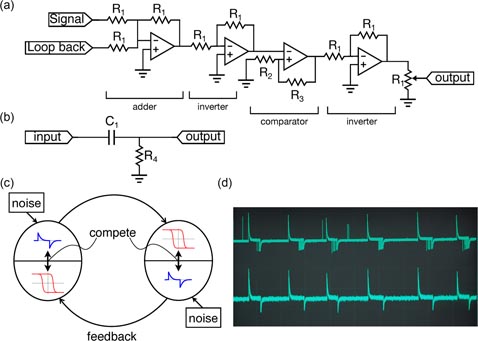
Figure 1. A single CE is implemented using a threshold element with hysteresis (TEH, (a)) and a delay derivative element (DDE, (b)). R1, R2, R3, R4, and C1 are 10 kΩ, 20 kΩ, 1 MΩ, 47 kΩ and 47 µF, respectively. We used quad operational amplifiers, TL084 (Texas Instruments), to the threshold element with hysteresis. The positive and negative electric power source used for the amplifiers was ±12 V. TEH is composed of four functional parts: the adder, inverter, comparator and inverter. All the resistors used here are standard metal-film resistors. A diagram for the ring circuit composed of two CEs (CEs, (c)) using McCulloch–Pitts neurons [16]. The typical time course for the ring circuit is shown in (d).
Download figure:
Standard image High-resolution imageNext, in numerical simulations, we used the following coupled Langevin equations (equation (1)) and (equation (2)):


where xi,
 and θ are output signal of ith element, element number, time, control parameters that define the potential, noise intensity, noise function, delay time and threshold value for TEH, respectively. The results of the numerical simulation using the fourth-order Runge–Kutta method are shown for the case of n = 4 (figure 2(a)). The detailed parameters used in the simulations are given in the figure caption. In the simulations, we performed numerical integrations with a Stratonovich interpretation [17–19]. Figure 2(b) shows a snapshot of emergent quasi-periodic signals, which are similar to those found in the above-demonstrated analogue electronic circuit. From a functional demonstration using the electronic circuit and numerical simulation, we found that spatio-temporal correlation in a multi-elemental system could be emergent from the collective dynamics of the stochastic elements, which was inspired from a mechanism of biological signal/information processing. At the same time, these demonstrations were, however, highly energy consuming processes, which was because the energy efficiency was quite low due to the utilization of noise with a much larger amplitude than neural systems. Furthermore, the numerical simulations were time consuming and also far from the real-time processing that would be easily realized in biological systems. Thus, this motivated us to realize the above-demonstrated devices using functional materials.

Figure 2. A ring circuit composing four CEs(#1-4). One CE is composed of a threshold element with hysteresis (TEH) and a delay-derivative element(DDE) (a). The typical time course of the four elements by numerical simulation by Langevin dynamics is shown (b). Mutually independent noise was applied to each element. Noise-driven oscillation, partial phase-locking and spontaneous phase-adjusting are visible. The parameters for the experiment were as follows: λ1:1, λ2:−0.1, λ3:−4, D:1000, η(t):GWN, τ:10, N:4, timestep:100, the number of points:10 000.
Download figure:
Standard image High-resolution imageFirstly we described a practical design for the basic device element using organic polymer materials. Figure 3 shows an illustration of the designed device element. We call the element a stochastic delay-derivative element (SDDE), which functions as a delay-derivative element and source of noise generation. To fabricate the SDDE, we focused on the two factors that could be important to characterize and control the stochastic behaviour of the element:
- (i)the phase separated structure of immiscible polymer binary mixtures and
- (ii)the crystallization behaviours of both binary components.
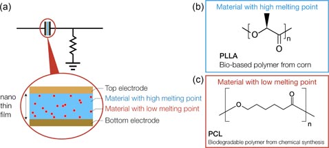
Figure 3. Schematic drawings for the designed delay-derivative element and for a polymer capacitor with fluctuated capacitance. Poly (L-lactide)(b), as a material with a high melting point, acts as ribs, and poly (ε-caprolactone)(c,) as a material with a low melting point, plays the role of an expected source of spatio-temporal fluctuation.
Download figure:
Standard image High-resolution imageIn this article, we used immiscible polymer blends between materials with a high melting point (Tm) and with low Tm (figure 3(a)). While the device is operated, the Joule effect associated with electric field application causes an increase in the device temperature. The device heating is expected to melt a material with low Tm. But the capacitor structure is preserved because a material with a high Tm acts as ribs. This partial melting of the binary mixture may cause the large spatio-temporal fluctuation on the capacitor that is a component of SDDE.
In this article, we selected poly (ε-caprolactone) (PCL) as a material with low Tm and poly(L-lactic acid) (PLLA) as a material with high Tm. The binary mixture of PLLA and PCL is known as a typical immiscible semicrystalline polymer mixture [20–23]. Since the melting temperature of PCL is about 60 °C [24, 25], the PCL component was used to endow the DDE with quasi-stochastic behaviour; that is, a noise generator based on a stochastic capacitor. As mentioned above, we gave attention to the phase separation and crystallization behaviours in polymeric nano-thin films and concentrated on the realization of the stochastic dielectric property of nano-thin films of the immiscible polymeric binary mixture.
2. Experimental section
2.1. Materials
The PLLA (LACEA, Mitsui Chemicals, Inc.; Mw = 3.4 × 10⁴ g mol−1, Mw/Mn = 1.64) and PCL (Cellgreen, Daicel Co.; Mw = 2.2 × 10⁴ g mol−1, Mw/Mn = 1.56) samples were characterized using gel permeation chromatography (HLC-8220GPC, TOSOH) using tetrahydrofuran. PLLA and PCL were purified using precipitation from a CHCl3/methanol mixture and drying in a vacuum at room temperature for 24 h. The samples were then stored in a vacuum desiccator at room temperature for 24 h.
2.2. Device fabrication
Figure 4 shows a schematic diagram for the device structure. All soda-lime glass substrates (S1111, Matsunami Glass Ind. Ltd, Japan) were successively cleaned with alkaline detergent, ion exchange water (10 min, ultra-sonication), acetone of semiconductor industry grade (10 min, ultra-sonication) and methanol of semiconductor industry grade (10 min, ultra-sonication), and then were preserved in methanol. Cr (thickness: 30 nm) and Au (50 nm) as a bottom electrode to a soda-lime glass substrate were deposited using a home-built thermal evaporator under vacuum (5 × 10⁻³ Pa). A two-layered electrode of Cr/Au is employed to gain the rigidity of the electrode. Nano-thin films on the substrates were prepared using the spin casting method (1500 rpm, 50 s; MS-A100, Mikasa Co. Ltd) of CHCl3 solutions (78 mg mL−1) of PLLA homo-polymer and PLLA : PCL binary mixture, respectively. Two kinds of the DDEs (abbr. LC1 and LC5; see the next section for details) were prepared, where the PCL contents were 1 wt% and 5 wt%, respectively. The film thickness was approximately 700–800 nm, which was determined from capacitance measurements and optical refractive index measurements using the Duc de Chaulnes method [26]. The obtained films were processed in line with the thermal programs shown in the next section. The top Au electrodes (50 nm) to the substrate were then deposited. All device elements were aged again at 5 °C for 24 h. The cross section of the vertical device element was 9 × 10⁻⁶ m2.

Figure 4. Schematic diagram for device (a). The device element with a type of crossbar junction forms a capacitor of Cr/Au/polymer/Au. Ag-paste was used to complete the contact with leads for measurements (b).
Download figure:
Standard image High-resolution image2.3. Thermal processing
Figure 5 shows the temperature programs for the fabrication of polymeric thin films. After spin casting, the elements were stored at 90 °C or 130 °C for 6 h under vacuum to complete the isothermal crystallization of the PLLA component. Then, the elements were cooled to 5 °C at a speed of 15 °C min−1 or 90 °C min−1 in order to control phase separation morphology of the amorphous region.

Figure 5. Temperature programs for polymeric thin films. TC is the isothermal crystallization temperature for the PLLA component. R is the cooling rate for the changing phase separation morphology of the fabrication of the polymeric thin films amorphous region.
Download figure:
Standard image High-resolution imageThe optional isothermal crystallization of PCL at 30 °C for 1 h was performed after the above-described cooling. Then, the elements were aged at 5 °C for 48 h in order to avoid further crystallization of the PCL. In this article, the device elements are indicated with the following abbreviations: 'PLLA' stands for a PLLA thin film and 'LC' denotes a PLLA and PCL polymer binary mixture. The number before 'LC' is the temperature of isothermal crystallization of PLLA. The number following 'LC' stands for the fraction for PCL. The alphabetical suffix 'g' or 'r' denotes a cooling speed of 15 °C min−1 or 90 °C min−1. The optional 'A' added at the end of the abbreviation is an element processed with the isothermal crystallization of PCL at 30 °C for 1 h. For example, 90LC5gA is the element with isothermal crystallization at 90 °C for 6 h after spin-coating, cooled at 15 °C min−1, aged at 30 °C for 1 h, cooled at 10 °C min−1, and aged at 5 °C for 48 h.
2.4. Atomic force microscopy
Atomic force microscopy (AFM) measurements at the damping mode were performed (Nanopics 1000, Seiko Instruments, Inc.). A sectional diagram in the Z-axis direction was determined after tilt correction based on the resulting profile curve of the surface.
2.5. Dielectric relaxation spectroscopy
Dielectric relaxation spectroscopy was performed using an LCR meter (4980A, Agilent) equipped with a home-built computer-controllable four channel scanner [27]. The details of the four channel scanner is shown in the online supplementary data (see section S1) (stacks.iop.org/JPhysD/47/365402/mmedia). The measurements were conducted over the frequency range of 20 Hz–2 MHz with a sinusoidal voltage of 100 mVp-p and over the temperature range from 30 to 90 °C at a step of 5 °C. A calibration standard of open/short/load was used for each frequency point. The complex conductivity σ*(= σ' + iσ'') was calculated from the complex impedance using the following relation:


where σ', σ'', d (= 700–800 nm) and A (= 9 × 10⁻⁶ m2) are the real and imaginary parts of σ*, the thickness of the polymer thin film, and the cross section area of the vertical device element, respectively. The complex relative dielectric constant ε*(= ε' − iε'') was calculated using the following model-free equation [28]:


where σ0 is the direct current conductivity. We used the model-free equation because the dielectric properties were investigated in potentially conductive samples due to nanometre-scale thin films. However, in reality, the contribution of σ0 was not subtracted from the data of ε'' because the contribution was obscure. The value of ε∞ was determined from the optical index using the Duc de Chaulnes method [26] and was treated as the dielectric constant at infinite frequency, ε∞.
2.6. Grazing incidence x-ray diffraction
We performed grazing incidence x-ray diffraction (GIXD) measurements. GIXD analysis was carried out on a Rigaku Rint Ultima III (Rigaku), working at 40 V and 40 mA, with Ni-filtered Cu Kα radiation (λ = 0.15418 nm). 2θ scans were made over an angle range of 5°–50° at a rate of 0.15 °min−1. In order to compare the PLLA : PCL mixture with PCL, we fabricated PCL thin films ('30PCL'), which are thin films isothermally crystallized at 30 °C for 1 h after a set of the spin-coating procedure at 1500 rpm, cooling at 15 °C min−1 and ageing at 5 °C for 48 h.
2.7. Noise measurements
In order to investigate the power spectral density (PSD) of time-fluctuation for SDDEs, we performed noise measurements, where the time course of electric current under a constant bias voltage was recorded on a digital storage oscilloscope (54621A, Agilent) equipped with a 10 MΩ detection probe (1000 points with a sampling dwell of 10 µs). The collected data of output voltages were transformed to currents using the input impedance. The current data were zero-filled to 1024 points and fast-Fourier transformed to generate PSD.
3. Results and discussion
First, we performed atomic force microscopy (AFM) measurements for various Cr/Au/polymer/Au elements, where the polymer was LC5, LC1 or PLLA. Figure 6(a) shows the AFM topographic image for 90PLLAg and 130PLLAg. For both 90PLLAg and 130PLLAg, spherulitic morphologies were visible. The crystalline nucleus density for 130PLLAg was lower than that for 90PLLAg, giving spherulites with a larger size. All data for the other elements are shown in the online supplementary data (see section S2) (stacks.iop.org/JPhysD/47/365402/mmedia). Furthermore, polarized optical microscopy (POM) observations give information about the spherulite growth rate of 2 μ m min−1 for 130PLLAg and of 0.5 μ m min−1 for 90PLLAg (see section S3 in the online supplementary data) (stacks.iop.org/JPhysD/47/365402/mmedia). The addition of PCL decreased the size of spherulites for PLLA (see section S2 and section S4). From these results, for PLLA : PCL mixtures, the difference in the growth rate of PLLA spherulite should cause a variation in the spatial distribution of PCL molecules, which accumulate in inter-lamella (ILA), inter-fibril (IFA) or inter-spherulitic amorphous (ISA) regions [29, 30] in the spherulite of PLLA. Figure 6(b) shows the topography cross section for the AFM data corresponding to the line indicated in the topography for 130PLLAg. There exist quasi-one-dimensional dips with a length of about 5 µm at the edge of the ISA regions, suggesting that the distance between the top and bottom electrodes in this region is much smaller than in the other portions of thin films. Therefore, the dielectric relaxation properties described later in this article should be influenced dominantly by the properties from the ISA region.
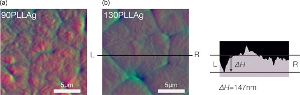
Figure 6. (a) An AFM topography image for 90PLLAg and 130PLLAg with the damping mode and (b) the topography cross section for the raw data corresponding to the line indicated in 130PLLAg.
Download figure:
Standard image High-resolution imageNext, we performed dielectric relaxation measurements for various Cr/Au/polymer/Au elements, where the polymer was LC5, LC1 or PLLA. Figure 7 shows the temperature dependence for the mean value, deviation and standard deviation of dielectric loss. It was found that the standard deviation (SD) of the variable frequency/temperature dielectric loss (ε'') varied depending on the cooling rate ('g' or 'r') after the isothermal crystallization process at 90 or 130 °C, and also depending on differences in the PCL fraction. It was also found that there were device-dependent fluctuations, even under the same experimental conditions for measurements using multiple device elements (the number of device elements was 2–5; see section S1 for the details). The value of SD is a direct measure of the device-dependent fluctuation.
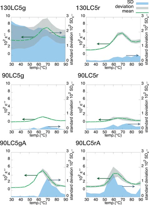
Figure 7. The temperature dependence for the mean, deviation and standard deviation of ε'' at an AC frequency of 10 kHz. The green solid line is the indicated mean of ε'' between the same experiment condition samples. The grey fill indicates the deviation between the maximum and minimum losses observed. The blue fill indicates the standard deviation (SD).
Download figure:
Standard image High-resolution imageThe peak area for the mean value of ε'' (the green solid line in figure 7) is assigned to the dielectric relaxation strength (Δε''). For the device elements without isothermal crystallization of PCL at 30 °C, the value of Δε'' was larger for 130LC than for 90LC. Since reorientational motions of the carbonyl group associated with the grass transition of PLLA should dominantly contribute to this relaxation, one possible scenario may be able to be pronounced; that is, a device element with the larger Δε'' should contain the more amorphous region (the lower crystallinity). If this is true, the total crystallinity near the ISA region for 130LC should be smaller than that for 90LC. However, since the size of a spherulite for 90LC is much smaller than that for 130LC, the effective cross section of the ISA region for the former was much larger than for the latter, implying that the more amorphous region for the former should contribute to the dielectric response. Moreover, the fraction for PCL should be increased in the ISA region for 90LC5, suggesting that the fraction of PLLA in the ISA region should be decreased. For 90LC5 elements, the size of the PLLA spherulites was smaller than those for 130LC5; that is, the fraction of inter-spherulites with respect to the whole volume of the thin film was larger for 90LC5. Nevertheless, the value of Δε'' was smaller for 90LC5 than for 130LC5, supporting the conjecture that the behaviour of Δε'' is dominated by the property of the ISA region. If the contribution from the ILA and IFA regions were also important, the DRS experiments should have shown a larger Δε'' for 90LC5, because 90LC5 has lower overall crystallinity than 130LC5 [31, 32].
Next, the blue-filled area shown in figure 7 stands for SD. For device elements without isothermal crystallization at 30 °C (the left and centre columns of figure 7), the gradually cooled elements showed larger SDs than the rapidly cooled ones except for 90LC5g (see the online figure S10 for the complete data set) (stacks.iop.org/JPhysD/47/365402/mmedia). The gradually cooled elements should facilitate the phase separation between PLLA and PCL, suggesting that the characteristic domain size of the phase separation should be larger than the rapidly cooled ones. This causes a larger PCL-rich domain in the ISA region. It is remarkable that 130LC5g shows the largest SD among gradually cooled elements. In the case of 90LC5, 90LC5g and 90LC5r show no differences or small fluctuations, even though for 90LC5 the largest amount of PCL molecules are segregated into the ISA region of PLLA among the fabricated device elements in this article. Additionally, this amount of PCL renders the PCL-rich domain enlarged. Since the crystallinity of PCL in the ISA region of PLLA would be therefore high, the SDs would become small due to the higher rigidity derived from the higher crystallinity of PCL in the ISA region.
Indeed, the results of grazing incidence wide angle x-ray diffraction (GIWAXD) support this view. Figure 8 shows the profiles of out-of-plane GIWAXD. For PLLA, the GIWAXD profiles for the samples crystallized at 130 and 90 °C show the same reflection peaks of (1 1 0)/(2 0 0) and (2 0 3) planes, but some minor peaks are visible for 130PLLAg [33, 34]. Then 30PCL shows two peaks around 21° and 23°. These peaks are assigned to the (1 1 0) and (2 0 0) planes [35]. While 130LC5r and 130LC5g show no PCL peaks, 90LC5r and 90LC5g shows some from PCL. All the data for the other elements are shown in the online supplementary data (see section S5) (stacks.iop.org/JPhysD/47/365402/mmedia).
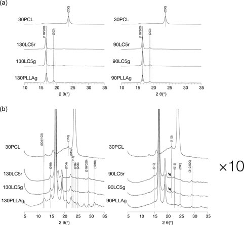
Figure 8. Out-of-plane GIWAXD profiles (a) and the expanded chart for vertical axis (b) for 30PCL, 130LC5g, 130LC5r, 130LC1g, 130LC1r, 130PLLAg. The arrows indicated the crystalline PCL.
Download figure:
Standard image High-resolution imageFor device elements with optional isothermal crystallization at 30 °C, Δε'' (right column of figure 7) was larger than those without the isothermal crystallization (centre column of figure 7). The SDs are larger around and over the melting point of PCL (Tm = 60 °C). Interestingly, the melting of crystalline PCL markedly affected to the value of Δε'' irrespective of small content of the PCL fraction. Furthermore, the value of Δε'' below the melting temperature of PCL is more or less the similar to those without isothermal crystallization at 30 °C. This means that existence of crystalline PCL reduces the valued SD probably due to rigidity of the elements. The isothermal crystallization at 30 °C would also induce further phase separation, resulting in larger SD over the melting temperature of PCL for elements with isothermal crystallization at 30 °C than those without the isothermal crystallization at 30 °C.
In order to gain further insights on the SDs, which could be due to the differences in heterogeneity (spatial fluctuations) of polymeric thin films in device elements and/or the differences in time-fluctuations in single device element, we performed noise measurements. Noise measurements provide direct information about the correlation function of time-fluctuations. The functional form of the power spectral density(PSDs) is one of crucial factors that affect on noise-driven signal transmission and spatio-temporal pattern formations [3, 4]. Figure 9 shows dependencies of averaged PSD at 10 kHz on temperature and applied dc voltages. The averaging was performed using five-times independent experiments. The elements of 130LC5g have the largest noise power at 10 kHz among device elements fabricated in this article (see section S6 for the other data). Therefore, the largest SDs for 130LC5g is attributed not only to the contribution from spatial fluctuation(heterogeneity) but also time-fluctuations. Isothermal dielectric measurements were performed as durability tests (see section S7 in the online supplementary data)(stacks.iop.org/JPhysD/47/365402/mmedia). Although the time course of dielectric property showed fluctuation with a certain extent, we did not observe notable asymptotic behaviours or degradation of the device elements during measuring time of over 40 h, meaning that the device elements fabricated in this article indicate some sort of durability to application of electric field.
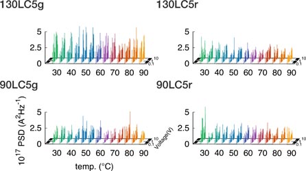
Figure 9. The dependence of the averaged power spectral density (PSD) at 10 kHz on temperature and applied dc voltages.
Download figure:
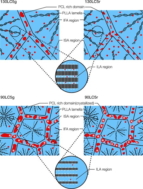
Standard image High-resolution imageFinally, we propose a plausible model for the morphology of LC5. Figure 10 shows a cartoon of the structural model for the polymeric binary mixtures of thin films. For elements of 130LC5g and 130LC5r, PCL molecules (red solid circles or domains) remain to some extent in the ILA and the IFA regions of the PLLA. The differences in cooling rate cause the difference in the phase separated structure of the PLLA : PCL mixtures. This affects the size of the PCL-rich domain in the ISA region (red domains). For gradually cooled elements, the phase separation between PLLA and PCL should progress, and therefore the size of the PCL-rich domain around the ISA regions would be enlarged, which in turn gains spatial- and time-fluctuations. Since for the rapidly cooled elements the phase separation should be limited because of vitrification of the PLLA fraction, the size of the PCL-rich domain around the ISA region would remain small, resulting in small SDs. As for elements of 90LC5, the slow isothermal crystallization of PLLA at 90 °C causes more segregated PCL molecules into the ISA regions. The cooling process also facilitates the further phase separation and therefore the enhanced size of the PCL-rich domain for gradually cooling around the ISA region. However there is no obvious difference in crystallinity of the PCL between 90LC5g and 90LC5r and the above-described reduced time-fluctuations.
Figure 10. Schematic drawings of a plausible model for the PLLA : PCL binary mixtures in the form of nano-thin films. The PCL molecules (red solid circles or domains) are likely to be remained in the ILA and the IFA regions of PLLA because of the faster spherulitic growth of 130LC than 90LC. The difference in the cooling rate causes the difference in the phase separated structure of the PLLA : PCL mixture. This affects the size of the PCL-rich domain around the ISA region of PLLA. Some portions of PCL-rich domains induce the crystallization of the PCL (red region with white spots).
Download figure:
Standard image High-resolution image
Stochastic capacitors like Cr/Au/130LC5g/Au are a candidate for the series capacitor part of an SDDE (see figure 1(b)). In this research, the typical capacitance (C) of the device element falls in the range of 0.1–1 nF. If one uses a parallel resistor of R = 1 GΩ, the delay time (τ = RC) falls in the range of 0.1–1 s. At the same time, the device current is more or less of the order of 1 nA. The delay time is comparable to that used for the demonstration using the analogue electric circuit (figure 1), meaning that the capacitor part of the electric circuit could be replaced by the device element developed in this research, if the input impedance and threshold voltage of a TEH are of the order of 1 MΩ and 10−2 V, respectively. If one will be able to fabricate a TEH with a threshold voltage of the order of 10−2 V using appropriate functional materials, a fully replaced CE using materials other than a conventional silicon semiconductor will be realized. Furthermore, there is the possibility that the inter-elemental variation of device properties enhances adaptive behaviour to input signals. Indeed, Kasai et al have recently reported that the variation of the threshold voltage for a GaAs-based etched nanowire field-effect transistor network enhances adaptability of the response to the input signal [36]. Therefore, the spatial fluctuation could play a positive role in a noise-driven signal processing network device. Additionally, although spatio-temporal correlation in the PLLA : PCL binary mixture remains elusive, control of the correlation might be accomplished by variation of the relative size of electrodes with respect to the size of a spherulite. If one can achieve the control of spatio-temporal correlation, a complex spatio-temporal pattern of activity of a network device that is composed of an ensemble of stochastic elements can be generated [12], which could lead to stochastic signal/information processing.
4. Conclusions
It is suggested that the dielectric relaxation behaviour is dominated by the reorientational dynamics around the ISA regions, which is induced by the difference in fabrication processes of devices. For device elements without isothermal crystallization at 30 °C, the value of Δε'' for elements with isothermal crystallization at 130 °C (130LC) is larger than those at 90 °C (90LC). The device elements of 130LC5g have the largest spatio- and time-fluctuations among elements fabricated in this article, which is probably due to the appropriate size of the PCL-rich domain to time-fluctuation. This suggests to us the existence of an optimized fraction of PCL for spatio-temporal fluctuations. This hypothesis is also supported by GIWAXD. For elements with an isothermal crystallization of PCL at 30 °C, Δε'' is larger than those without isothermal crystallization at 30 °C. This suggests that the melting of PCL as well as the glass transition of PLLA affect Δε'' and also SDs.
Conclusively, we found that the stochastic delay-derivative element (SDDE) using a PLLA : PCL binary mixture showed spatio-temporal fluctuations that depended on the fabrication processes of cooling rate and PCL fraction. The currently fabricated DDE would be a possible candidate for SDDE that is useful for bio-inspired noise-driven signal/information processing devices.
Acknowledgments
This work was supported by the Japan Society for the Promotion of Science (JSPS) KAKENHI Grant-in-Aid for Challenging Exploratory Research Number 24655093.