
Abstract
In this work, we propose a resonant tunnelling diode (RTD) based on a double-barrier graphene/boron nitride (BN) heterostructure as a device suitable to take advantage of the elaboration of atomic sheets containing different domains of BN and C phases within a hexagonal lattice. The device operation and performance are investigated by means of a self-consistent solution within the non-equilibrium Green's function formalism on a tight-binding Hamiltonian. This RTD exhibits a negative differential conductance effect, which involves the resonant tunnelling through both the electron and hole bound states in the graphene quantum well. It is shown that the peak-to-valley ratio reaches a value of ∼4 at room temperature even for zero bandgap and can be higher than 10 when a finite gap opens in the graphene channel.
Export citation and abstract BibTeX RIS
1. Introduction
The benefits of the extraordinary intrinsic transport properties of graphene [1] are usually hindered by the defects of the supporting insulating substrate. In fact, graphene on various substrates such as SiO2 [2], SiC [3] or other high-κ insulators [4] shows a reduced carrier mobility, which is usually attributed to surface roughness, charge surface states or surface optical phonons. Recently, it has been shown that graphene supported on hexagonal boron nitride (h-BN) has higher mobility than on any other substrate [5–7]. A mobility of 275 000 cm2 V−1 s−1 at low temperatures and 125 000 cm2 V−1 s−1 at room temperature, i.e. as high as that of suspended graphene, has even been reported [8]. It is due to the fact that the surface of h-BN is flat, with a low density of charged impurities, does not have dangling bonds and is relatively inert [5]. Hence, with the same atomic structure as graphene and a 1.8% higher lattice constant [9] h-BN is becoming a very promising candidate as a high bandgap insulating material to achieve the ballistic transport regime in graphene devices even at room temperature and exploiting the peculiarities of graphene properties inherent in the massless and chiral character of charge carriers.
Additionally, hybrid structures consisting of a mixture of BN and carbon nanodomains have been recently realized [10, 11]. In [10], Enouz et al reported on the synthesis of C-BN single-walled nanotubes made of BN nanodomains embedded into a graphene layer using a continuous CO2 laser vaporization reactor. In particular, Ci et al in [11] used a thermal catalytic chemical vapour deposition method to synthesize 2D monolayers consisting of large BN domains in graphene. Together with rapid progress in technology, one can optimistically expect that these structures can be well controlled on the atomistic scale soon. Hence, the experimental results above are particularly valuable in terms of electronic applications of graphene, as they provide a new way to induce and engineer the bandgap in this 2D material [12]. They have recently stimulated investigations on the electronic properties of many different graphene/BN heterostructures, e.g. see [13–18].
In the field of quantum devices, graphene resonant tunnelling diodes (RTDs) have been proposed and investigated previously [19, 20]. However, while the operation of graphene nanoribbon RTDs is strongly dependent on the device shape and the edge effects [19], the 2D graphene structures studied in [20] are based on the assumption that a bandgap opens in graphene epitaxially grown on SiC, which has a drawback of substrate-induced mobility reduction. In this work, we therefore propose a new graphene RTD using graphene/h-BN heterostructures, where the two barriers are formed by h-BN zones with a large bandgap, as schematized in figure 1. Although it may be useful and possible in the case of Bernal stacking on a BN substrate [21, 22], we will show later that the bandgap in graphene is not necessary for this device to operate correctly.
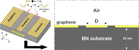
Figure 1. Simulated resonant tunnelling device wherein the graphene sheet is supported on a h-BN substrate and two barriers are formed by BN domains inserted in the graphene layer.
Download figure:
Standard imageTo investigate the operation of this RTD, we have developed a self-consistent simulation code based on the Green's function formalism [23] within the tight-binding model constructed in [17].
2. Simulated device and approach
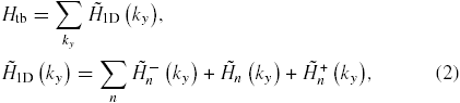
In the simulated RTD (see in figure 1), the two BN barriers are inserted into a monolayer graphene sheet, which is supported on a h-BN substrate. The charge transport in the device channel is considered using the tight-binding model in [17], which is parametrized from ab initio calculations. The approach was demonstrated as a simple and efficient method to explore well the electronic properties of the considered graphene/BN heterostructure. This tight-binding Hamiltonian of charge carriers has the form

where tnm denotes the hoping energy between the atomic (carbon, boron and nitride) sites [17] and Un is the onsite energy/potential energy at the nth site. This potential energy is determined by solving the Poisson equation self-consistently with the equation of Green's function as mentioned below. We assume the transverse width along the OY direction to be much larger than the typical device length along the transport direction, i.e. a few tens of nanometres, so that the extension along the transverse direction can be considered through Bloch periodic boundary conditions [23]. To conveniently study the charge states, the considered lattice is split into elementary cells (see figure 1) and, using the same approach as in [23], we Fourier transform the operators in equation (1) along the OY direction. Hamiltonian (1) is then rewritten in terms of decoupled (quasi-1D) forms
where
 is the Hamiltonian of cell {n} and
 denotes the coupling of cell {n} to cell {n ± 1} along the transport (OX) direction.
Using Hamiltonian (2), the device retarded Green's function in the ballistic approximation is computed for a given momentum ky as

where Σ(ky) = ΣL(ky) + ΣR(ky) with the self-energy ΣL(R) describing the device-to-left (right) contact coupling. The local electron density in the graphene/BN sheet is then determined by [24]
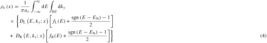
in which the local density of states (LDOS) resulting from the left/right injected states is calculated using DL(R) = GΓL(R)G†/2π with the injection rate
![$\Gamma_{\rm L(R)} = {\rm i}[ {{\Sigma _{{\rm L(R)}}} - \Sigma _{{\rm L(R)}}^\dagger} ]$](https://content.cld.iop.org/journals/0022-3727/45/32/325104/revision1/jphysd427668ieqn003.gif) ; ax is the distance between two nearest cells along the OX direction, EN is the charge neutrality level, fL,R(E) are the left and right Fermi distribution functions with Fermi levels EFL and EFR, respectively. This electron density is fed back into the Poisson equation for a self-consistent solution. Once self-consistence is achieved, the current density is computed by
; ax is the distance between two nearest cells along the OX direction, EN is the charge neutrality level, fL,R(E) are the left and right Fermi distribution functions with Fermi levels EFL and EFR, respectively. This electron density is fed back into the Poisson equation for a self-consistent solution. Once self-consistence is achieved, the current density is computed by

where the transmission coefficient
 and the integral on ky is performed in the first Brillouin zone.
In our simulation, the Poisson equation is solved in the domain bounded by the boundaries (dashed lines seen in figure 1) where the null Neumann conditions are applied. Its solution of potential energy in the graphene/BN sheet is then fed back into Hamiltonian (1). The iterative loop of the Green function and the Poisson equations is repeated until the self-consistence is achieved. Note that in the case of Bernal stacking, graphene on a h-BN substrate was shown to exhibit a finite bandgap, but this bandgap vanishes when graphene is misaligned with respect to the h-BN lattice [21, 22]. Therefore, unless otherwise stated, zero bandgap of graphene was assumed in our study. All simulations were performed at room temperature.
3. Results and discussion
Our simulations were performed for RTDs wherein a h-BN substrate of thickness 10 nm and dielectric constant εr ≃ 3.5 [5] was used. The graphene sections (including the emitter, the collector and the access region of length 17 nm) in both device ends are heavily n-doped while the thickness of the BN barriers was assumed to be 1.3 nm. The active region sandwiched between the two doped zones is undoped. Doped graphene can be realized using polyethylene imine and diazonium salts [25], hydrogen silsesquoxane films on graphene [26], substitutional donors (nitrogen) or acceptors (boron) [27], or other different methods reviewed in [28].
In figure 2, self-consistent solutions of potential energy and electron density are plotted for different biases applied to the device with well width D = 4.3 nm and doping concentration in access regions ND = 5 × 10¹⁶ m−2. The low doping in the central zone generates a potential barrier, which controls the threshold voltage of the device. Differently from the conventional RTDs [29], figure 2(b) shows that the local charge density is not symmetric even at zero bias. This feature can be understood as a consequence of the device asymmetry between the left graphene section coupled to nitrogen atoms and the right section bounded to boron atoms of the h-BN lattice. In addition, it is shown that the electron density accumulated in the quantum well (QW) increases when the bias voltage is increased from 0 to 0.4 V and decreases when the bias is further raised from 0.4 to 0.6 V. This feature is nothing but an effect of resonant tunnelling [29] as discussed below.

Figure 2. (a) Self-consistent profiles of potential energy and (b) corresponding electron density for different applied biases. The doping concentration in both device ends is ND = 5 × 10¹⁶ m−2. The vertical dashed lines indicate the graphene/h-BN junctions.
Download figure:
Standard imageWe now go to explore the electrical behaviour of the device. In figure 3, we display the I–V characteristics together with diagrams showing the LDOS and the corresponding transmission coefficient at different applied biases. In fact, the diagrams in figures 3(a)–(c) show that the h-BN barriers with a large bandgap (≈3.9 eV [17]) generate the quantization of carrier states in the graphene QW, which gives rise to strong resonant tunnelling effects in the transmission coefficient. As a consequence, the I–V curves can exhibit a strong negative differential conductance (NDC) in both cases of gapless and gapped graphene. We should bear in mind that in principle, the valley current occurs at a finite bias when the resonant level in the QW is in front of the bandgap of the emitter and the resonant current is thus switched off. This is not exactly the same case in the device considered here when the graphene bandgap (bandgap of the emitter) is zero. The observed NDC effect is explained as follows. Although the valence band of graphene touches its conduction band at the Dirac point corresponding to
 , a finite energy gap
 still appears for other momenta ky ≠ Ky (see in [32]), where tCC = 2.5 eV [17] and ac is the carbon–carbon distance. For instance, for
 ,
,
 , which is illustrated by the energy width of the blue zones in the two device ends of the LDOS diagram in figures 3(a)–(c). Since the total current results from the contribution of all different momenta ky, a deep current valley occurs even in gapless graphene devices (see figure 3(d)) when the tunnelling corresponding to the large values of |ky − Ky| is suppressed (due to the energy gap
 mentioned above) at high bias. In fact, it is clearly illustrated in figure 3 that for
 , the resonant peak numbered (1) at Vbias = 0.4 V (see in figure 3(a)) disappears at Vbias = 0.6 V (see in figure 3(b)). In addition, the ky-dependence of such a resonant peak at Vbias = 0.6 V is demonstrated in the inset of figure 3(b), i.e. the transmission coefficient is high for ky around Ky but almost suppressed when |ky − Ky| is large enough. Moreover, because of the zero (or small) bandgap of graphene, it is also shown that the current valley in this device is much narrower than that in conventional RTDs [29]. When introducing a finite bandgap [21, 22, 30, 31] in graphene, both the valley and peak currents are of course reduced while the peak-to-valley current ratio (PVR) increases. The latter reaches ∼4, 13 and 17 for bandgaps Eg = 0, 50 and 100 meV, respectively. Such high PVR values are significant in comparison with the best value obtained at room temperature in other graphene RTDs [19, 20] and in conventional semiconductor devices [29].
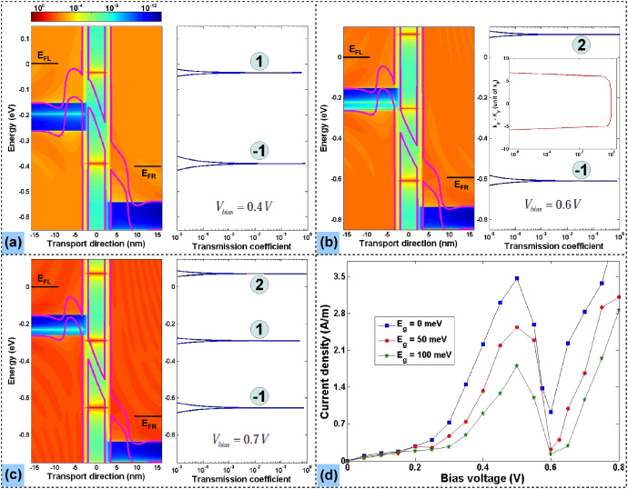
Figure 3. (a), (b), (c) Diagrams showing the LDOS (left) and the transmission coefficient (right) as a function of energy at different applied biases and (d) I–V characteristics of the simulated device for different graphene bandgaps. The figures in (a), (b), (c) are plotted for a transverse momentum ky ≠ Ky (Ky is the momentum at the Dirac point, see discussions in the text) and for gapless graphene. Numeral indices indicate the confined levels for which the resonant tunnelling appears while the signs (+/−) correspond to the electron/hole states. The inset of (b) shows the ky-dependence of the transmission peak via the confined level numbered (1) at Vbias = 0.6 V, where
 . The corresponding electron/hole potential profiles (solid lines) are superimposed on the LDOS. The doping concentration is ND = 5 × 10¹⁶ m−2.
Download figure:
Standard imageIn particular, from figure 3, we find an interesting feature: differently from other RTDs [19, 29], where only the electron states in the QW are involved in the resonant tunnelling, here due to zero (or small) graphene bandgap, both electron and hole states can contribute to the current. This point has also been discussed in [33] and was shown to reduce the NDC effect in single potential barrier graphene structures. Practically, as we can understand from figure 3(a), the confined hole states in the QW make the tunnelling from the hole states in the emitter to the electron states in the collector possible. This band-to-band (BTB) process (numbered (-1)), in addition to the normal resonant tunnelling (numbered (1)) of electrons via the electron states in the QW, contributes to the rapid increase in current beyond Vbias = 0.25 V. The vanishing of the latter process (see figure 3(b)) is responsible for the valley regime in the I–V characteristics. When Vbias is further increased, the BTB tunnelling through the first electron level in the QW occurs (see the resonant peak numbered (1) in figure 3(c)), which leads to the rapid re-increase in current and a narrow current valley, as seen in figure 3(d).
To evaluate the role of device parameters on the RTD operation, we display in figures 4(a) and (b) the I–V characteristics obtained for different doping concentrations ND in the access regions and for different well widths D, respectively. Actually, when ND is increased, the flat potential profile in the two doped access zones (see in figure 2(a)) moves down in energy and the valley current hence occurs at a higher bias voltage. In addition, the contribution of BTB resonant tunnelling, which is more important at high bias, makes both the peak and valley currents higher with increasing ND. This finally reduces the PVR, i.e. it reaches ∼3.9, 3.8, 2.2 and 1.8 for ND = 2.5 × 10¹⁶ m−2, 5.0 × 10¹⁶ m−2, 7.5 × 10¹⁶ m−2 and 1017 m−2, respectively. Figure 4(b) shows that when the well width D is increased, the current valley shifts towards low bias while the NDC effect generally weakens. This feature can be straightforwardly understood as the influence of D on the energy spacing and number of energy levels in the QW. In the case of large D (e.g. 6.4 nm in figure 4(b)), the multi-level contribution gives rise to a quite complex I–V curve with a low PVR.
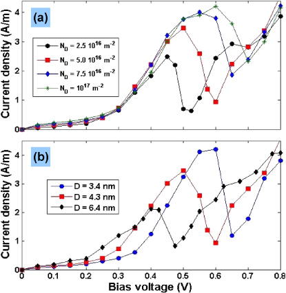
Figure 4. I–V characteristics (a) for different doping concentrations ND in both device ends and (b) for different well widths D; D = 4.3 nm in (a) and ND = 5 × 10¹⁶ m−2 in (b).
Download figure:
Standard imageFinally, though not shown here, the overall current appears to be strongly reduced when the BN barrier thickness is increased, as a consequence of the large bandgap of h-BN. It, therefore, suggests that to clearly observe the effects discussed above, a barrier thickness smaller than 2 nm is mandatory.
Note that all results presented in this paper were obtained in devices with perfect edges between graphene and BN sections. Since the precise control of these edges on the atomistic scale is still a technological challenge, edge disorder may occur and affect the transport characteristics of the device. However, differently from the case of disordered graphene nanoribbons (e.g. see in [34]), wherein the rough edges are parallel to, they are perpendicular to the transport direction here. The edge disorder makes the width (along the OY direction) of graphene QW and BN barriers inhomogeneous, which can affect the position of confined levels in the QW. Though not shown here, we find that in spite of such a feature, the main (resonant and NDC) effects in this kind of device are not strongly influenced except in the case of too strong disorder making the device geometry (i.e. QW and barriers) very complicated.
4. Conclusion
In summary, a numerical simulation of graphene RTDs based on graphene/h-BN double-barrier structures was performed by means of the self-consistent solution of the Poisson and Schrödinger equations within the tight-binding model. It was shown that the resonant tunnelling and the resulting NDC behaviour may involve both the electron and hole bound states in the graphene quantum well. The sensitivity of the electrical characteristics to the device parameters such as the doping density of access zones, the QW thickness and the barrier thickness was analysed. Although the band-to-band tunnelling tends to reduce the width of the valley region in the I–V characteristics and to induce a rapid re-increase in current, the PVR of NDC effect reaches a value of ∼4 at room temperature even for zero bandgap and can be higher than ten when a finite gap opens in graphene, which may result from Bernal stacking of graphene on h-BN. This work suggests that the engineering of graphene/h-BN structures is opening a new route for high-performance graphene devices.
Acknowledgments
This work was partially supported by the French ANR through the projects NANOSIM-GRAPHENE (ANR-09-NANO-016) and MIGRAQUEL (ANR-10-BLAN-0304). One of the authors (V H N) thanks the Vietnam's National Foundation for Science and Technology Development (NAFOSTED) for financial support under the Project No 103.02-2010.33.