

Abstract
A printable mesoscopic ceramic framework and commercial carbon based perovskite solar cell was fabricated. NiO mixed with graphene was used as hole-transport materials to improve the hole-extracting ability in the mesoscopic ceramic framework and carbon based perovskite solar cell. FESEM, XRD, and contact angle tests were used to investigate the morphology and structure of the mesoscopic ceramic framework. The open-circuit voltage attenuation, photocurrent-time, and other methods showed that the charge transfer capability inside the device was greatly improved after the addition of NiO/graphene. The appropriate pore size of the top HTM layer using NiO/graphene with a mass ratio of 100:1 provides the effective and direct channel for perovskite arriving at the TiO2 electron collection layer. The contact angle of the water on the surface of the mixed NiO/graphene was greatly increased, preventing perovskite from water vapor erosion. The photoelectric conversion efficiency of the device using NiO/graphene as the hole transport material is 11.72%, showing 33% increase when compared with HTM-free devices. In addition, the PCE of the carbon-based solar cell maintained 91% of the original value after one week due to the hydrophilicity of the composite NiO/graphene material.
Export citation and abstract BibTeX RIS
The Organic-inorganic halide perovskite solar cells (PSCs) have attracted much attention because of the large light absorption coefficient, bipolar carrier mobility, and long electron-hole pair diffusion length. 1 Since 2009, it has been reported for the first time that CH3NH3PbI3 is used as a light-absorbing material for solid-state solar cells. The photoelectric conversion efficiency (PCE) has increased from 3% 2 to 25.2% 3 in just 9 years, which has undoubtedly become a breakthrough in photovoltaic technology since the 1970s. Despite the rapid development of the efficiency of PSCs, there are still some pressing issues that need to be addressed, such as heat and moisture instability and excessive manufacturing costs 4 . Nowadays, high-efficiency PSCs use expensive organic HTM, 5 such as Spiro-OMeTAD, 6 PEDOT: PSS, 7 PTAA, 8 etc. They are easy to absorb water, and decompose perovskite absorber layer, which has a large negative impact on the long-term stability of the device. 9
Due to the good electrical conductivity, good hydrophobic properties, and suitable work function of carbon materials, 10 Han, 11 and others used carbon as the counter electrode instead of expensive Au/Ag, which greatly reduced the cost of PSCs. According to Meng, 12 perovskite has good bipolar semiconductor properties. They can not only act as light absorbers but also can replace holes transporting materials with efficiently transport holes, thus removing organic HTM. At present, the highest PCE of PSC based on carbon materials as the counter electrode has exceeded 17%. 13 Although the organic HTM requires complex synthesis processes and expensive price requirements, its efficient collection of holes is unquestionable. To promote the PSCs to large-scale industrial applications, scientists have proposed the use of inexpensive inorganic types. Inorganic HTM is used as a substitute, such as NiO 14,15 and CuSCN, 16 which combines low cost, good carrier transport properties, and chemical stability. NiO has a wide bandgap, whose conduction band is −1.8 eV, compared with −3.39 eV of MAPbI3. Besides, it has good thermal and chemical stability, thus it is most widely used as inorganic HTM in mesoporous or planar PSCs for inverted structures. 17 Besides, Cu doping can also be used to improve the conductivity of NiO, 18 and the combination of metal (Li, Mg) or PEDOT to modify NiO. 19 In the TiO2/ZrO2/C full-print mesoscopic PSCs, Wang used p-type NiO nanoparticles to replace part of the ZrO2 insulating layer to improve the hole transporting ability of the device, so that the PCE of carbon-based PSC increased by 39% and received 17% of PEC. 20
Due to the different bonding modes of carbon atoms, carbon materials can be classified into many different types. Such as graphite, carbon black, carbon nanotubes, graphene, and its derivatives. 21 Carbon materials with a continuous structure, especially carbon nanotubes 22 and graphene, 23 not only have high electrical conductivity but also provide direct charge transport channels, making them an additive or even a substitute for HTM in PSCs. 24 Wang et al. 25 have reported that SWCNTs are mixed in the counter electrode of NiO to improve the conductivity and the extraction rate of holes to replace the traditional carbon-based pair. The electrode greatly reduces the thickness of the device. 2D structure of graphene (GR), its derivatives graphene oxide (GO) and the reduced graphene oxide (RGO) are versatile materials with large theoretical surface area, active internal charge, and good thermal conductivity. Yang 26 proposed applying graphene to HTM, which can increase the collection rate of photogenerated holes and improve the PCE of PSCs. 27
In this study, to improve the efficiency of mesoscopic carbon-based ceramic framework perovskite solar cell, the NiO film was prepared as HTM in the mesoscopic carbon-based ceramic framework perovskite solar cell of TiO2/Al2O3/NiO/C. However, the thickness of the Al2O3 and NiO e insulator ceramic layer exceeds 1 μm, which may affect the internal charge transfer from NiO to carbon layer because since NiO has low electrical conductivity. Therefore, to improve the conductivity and hole extraction ability of the inorganic HTM, a small amount of graphene is added into the NiO slurry, which effectively improves the PCE of the device and the stability of the device in the air.
Experimental
Preparation of slurry
The solid powder of Al2O3 and ethylcellulose were weighed according to the mass ratio of 2: 1, and a proper amount of ethanol was added, stirred for 5 min and sonicated for 10 min. Terpineol was added into the mixture to make the solid content reaching to 10%. The mixture was stirred for 5 min and sonicated for 10 min. Then it was ball milled for 10 h. The slurry is finally heated to remove ethanol. The same method was used to prepare NiO slurry. Different amounts of graphene were added into the NiO slurry, followed by the addition of terpineol to control 15% solid content in the mixture. Carbon slurry was prepared by using the mass ratio of graphite: carbon black: ethylcellulose: zirconia = 7:2:1:1, diluted with ethanol and ball milled for 10 h.
Preparation of the mesoscopic ceramic framework
The FTO substrate was put into an ultraviolet ozone machine for ozone treatment for 30 min to remove the surface organic matter. A 0.15 M solution of titanium diisopropoxy acetonate in n-butanol was spin-coated on an FTO substrate at 2000 rpm and dried at 125 °C. The dense layer was calcined at 450 °C for 30 min. The dense layer of TiO2 was immersed in a 40 mM aqueous solution of titanium tetrachloride for 35 min at 70 °C, then rinsed with deionized water and ethanol three times and dried at 500 °C for 30 min. The mesoporous layer was spin-coated by using a TiO2 slurry at a speed of 2,500 rpm for 30 seconds. The mesoporous layer was dried at 125 °C and calcined at 500 °C for 30 min. The Al2O3 and NiO paste were screen-printed to the mesoporous substrate and dried at 120 °C for 10 min. The mesoscopic ceramic framework was calcined at 500 °C to remove organic impurities. The carbon paste was printed onto the mesoscopic ceramic framework layer with a 200 mesh screen and dried at 120 °C for 10 min, followed by calcination at 400 °C for 30 min.
Preparation of perovskite
Two-step preparation of perovskite: preparation of 0.48 mg μl−1 lead iodide DMF and 10 mg ml−1 iodomethylamine. Drop the lead iodide solution at 70 °C from the top of the carbon layer. When the lead iodide solution has penetrated completely, dry the base at 70 °C for 30 min. After cooling to room temperature, soak the base in a 10 mg ml−1 iodomethylamine solution for 10 min. After washing the residual iodomethylamine on the surface of the base with isopropanol, dry it at 70 °C for 30 min.
Characterization
The morphologies of NiO, graphene, and the whole cell were measured by a Hitachi S-4800 field emission scanning electron microscope (FESEM). The crystalline phase of the perovskite was examined by X-ray diffraction (XRD, SmartLab, Rigaku). Photocurrent and voltage were measured by a Keithley 2400 source meter, and a solar simulator (Oriel 94023 A) equipped with a 450 W xenon lamp (Newport 6279NS). The output power was adjusted to match AM 1.5 global sunlight, which was calibrated by a certified reference silicon solar cell with the intensity of 100 mW﹒cm−2 before use. The voltage scan rate was 10 mV s−1, and no device preconditioning was applied before starting the measurement, such as light soaking or forward voltage bias applied for a long time. The directions were reverse scan mode (1.0 V to −0.1 V) and forward scan mode (−0.1 V to 1.0 V), respectively, and the dwell time is 15 ms. The starting voltage was determined as the potential at which the cells furnish 1 mA in forwarding bias, no equilibration time was used. The cells were masked with a black metal mask (0.04 cm2) to obtain the active area and reduce the influence of the scattered light. All these procedures were carried out in a naturally ambient atmosphere. In the frequency range of 1 Hz to 100 kHz, the AC amplitude is 5 mv for EIS measurement. A Lambda 950 spectrophotometer was used for ultraviolet–visible (UV–vis) spectrum measurement.
Result and Discussion
Figure 1a is a cross-section FESEM image of the Al2O3 spacer layer. As seen from Fig. 1a, the thickness of the spacer layer is 500 nm, and the film thickness is uniform with no agglomeration. Figure 1b shows a 1 μm NiO hole-transport layer, which is a screen printed on Al2O3 spacer layer by a 400 mesh screen. Al2O3-NiO interface is closely connected, and the overall thickness is up to 1.5 μm. Figure 1c is a plan view of the HTM layer prepared by NiO nanoparticles and graphene. NiO nanoparticles are about 20 ∼ 30 nm with no agglomeration in the hole transfer layer. The film has a proper amount of voids, indicating that PbI2 can easily and fully penetrate the porous viods. Figure 1d is a FESEM image of graphene nanosheets, and all of them are within 1 μm. Graphene nanosheets with different sizes can be filled into the NiO HTM layer and without large pores or accumulation. Figures 1e and 1f show the front and side view of the HTM layer prepared by the mixed NiO and graphene with a mass ratio of 100:1. It can be seen from the cross-sectional FESEM image that the graphene is dispersed in the mixed NiO/graphene HTM layer without agglomeration, which increase the conductivity ability of NiO and benefit for the hole extraction.

Figure 1. Cross-sectional FESEM image of (a) Al2O3 spacer layer (b) Al2O3 and NiO HTM, Plane-viewed FESEM image of (c) NiO HTM, (d) graphene, (e) NiO mixed graphene HTM, (f) Cross-sectional FESEM image of NiO mixed graphene HTM.
Download figure:
Standard image High-resolution imageFigure 2 shows the XRD picture of the hole transporting material of the mixed NiO and graphene used in the experiments in this paper. It is apparent that the diffraction peaks of nickel oxide are 2θ of 37.4°, 43.3°, 63.0°, and 75.6°, corresponding to NiO crystal plane of (111), (200), (220), (331). 28 The XRD of graphene does not show a distinct peak position since graphene is a single-layer carbon material and has no obvious crystal form. The diffraction peak of graphene located at the same position of the diffraction peak of graphite.

Figure 2. XRD patterns of NiO NPs and Graphene.
Download figure:
Standard image High-resolution imageFigure 3 shows the mapping spectrum of the mixed NiO/graphene with a mass ratio of 100:1. The Si and Sn elements in Fig. 3 are derived from conductive FTO glass, and the O and Ni elements are derived from NiO nanoparticles. The C element is derived from graphene. It can be seen from Fig. 3 that the content of graphene is small, graphene was uniformly dispersed in the NiO film, which greatly enhanced the conductivity ability of NiO and benefit for the hole extraction.

Figure 3. Mapping spectrum of NiO HTM mixed with graphene.
Download figure:
Standard image High-resolution imageDropping PbI2 solution into the mesoscopic ceramic framework plays a vital role in the fabrication of the device. To allow the solution to penetrate smoothly into the mesoscopic ceramic framework layer of the device, it is necessary to characterize the pores of the top HTM layer. Table I shows that the average pore diameter of the Al2O3 nanoparticles is 24.8 nm. To further investigate the pore size of the top HTM layer, the adsorption and desorption and surface area test of the mixed NiO/graphene are carried out. Figures 4a–4c are N2 adsorption-desorption curves of the mixed NiO/graphene with a mass ratio of NiO: GR = 1:0, 100:1, 150:1, respectively. It can be seen from Figures 4–2d, the pore diameter of the NiO nanoparticles is 19.92 nm, which is smaller than that of the Al2O3 mesoscopic ceramic framework layer, indicating that perovskite infiltrated into the mesoporous layer is affected. The increased specific surface area and pore size of the top NiO/graphene HTM can be ascribed to the doping concentration of graphene, which give the direct channel for the filling of the perovskite into the down layer. Also, the larger specific surface area of the top HTM layer indicates more contact of HTM layer with the perovskite absorbing layer, which is benefit for the collection and separation of holes. 29 As can be seen from the above data, it can be seen that the pore diameter of the top HTM layer is 24.19 nm when the mass ratio of NiO/graphene is 100:1, which is similar to the pore size of the Al2O3 spacer layer. The similar pore size of the top HTM layer and the down mesoscopic ceramic framework layer provide the effective and direct channel for perovskite arriving at the electron collection layer.
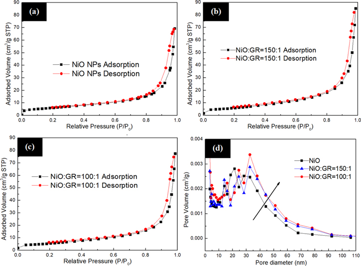
Figure 4. (a)–(c) N2 adsorption-desorption curve of NiO/graphene and (d) BJH pore size distribution curve.
Download figure:
Standard image High-resolution imageThe stability of the perovskite light-absorbing material in the air is greatly influenced by the water vapor, the hydrophilicity of each layer of the device has great damage to the stability of the device, which easily leads to the decomposition of the perovskite. Figure 5a shows the hydrophobicity test of the contact angle of water on NiO film. It is found that NiO nanoparticles have great water absorption. If the device is placed in the air for a long time, the device will be affected by the water absorption of NiO, which will decompose CH3NH3PbI3 into PbI2. Figure 5b shows the contact angle test of water on the mixed NiO/graphene film. It is found that the contact angle is greatly increased, indicating that the mixed NiO/graphene film layer is prevented perovskite from water vapor erosion. 30 However, when the PbI2 solution is dispensed, N-N-dimethylformamide (DMF) is used as a solvent. If the contact angle of NiO/graphene with DMF is too large, the perovskite precursor could not penetrate the mesoporous layer. Therefore, DMF was used as the wetting liquid and test the contact angle (Figs. 5c, 5d). It was found that the addition of graphene does not affect the infiltration of PbI2, mainly because the surface tension of DMF is small.

Figure 5. The contact angle test of water on (a) NiO film (b) NiO/graphene film; the contact angle test of DMF on (c) NiO film (d) NiO/graphene film.
Download figure:
Standard image High-resolution imageFigure 6a shows the cross-sectional FESEM image of the solar device. The cross-sectional FESEM images clearly show the solar cell consisted of 500 nm mesoporous layer TiO2, 500 nm spacer layer Al2O3, and the 1 μm NiO/GR hole transport layer, the top layer is carbon layer with a thickness of ∼10 μm using as the contact electrode. Figure 6b is a schematic view of the structure of the battery. Figure 6c shows the energy band structure of the battery and the transport direction of the carriers inside the perovskite. Because the conduction band of the ETL layer TiO2 is lower, so electrons are transported into TiO2. The remaining holes are transported from the perovskite valence band to the NiO valence band and eventually collected by the contact electrode of carbon layer. 31 Figure 6d shows the XRD pattern of a PSC prepared by containing different amounts of graphene in the hole-transport layer. The thickest carbon layer is on the uppermost layer, the diffraction peaks of graphite can be seen. The diffraction peaks of hexagonal perovskites located at 2θ: 14.5°, 20.4°, 23.5°, 24.7°, 28.7°. 32.3° and 34.7°, corresponding to (110), (112), (211), (202), (004), (310), and (312) crystal faces of the cubic phase CH3NH3PbI3, respectively. 32 However, the difference is that in the XRD pattern of NiO/graphene with a mass ratio of 50:1, the diffraction peak of PbI2 is significantly higher than the other two spectra. It is indicated that the full penetration of the PbI2 precursor solution was hindered by excessive graphene, thus resulting in the incomplete reaction of PbI2. When the mass ratio is 100:1, the penetration of PbI2 solution into the mesoporous layer of the device is not affected.

Figure 6. (a) Cross-sectional FESEM image of the Device and (b) Schematic diagram of FTO/TiO2/ Al2O3/ NiO/C, (c) Energy diagram of the solar cell, (d) XRD of perovskite solar cell.
Download figure:
Standard image High-resolution imageTable I. BET plot.
| Parameters | Al2O3 | NiO | NiO: GR = 150:1 | NiO: GR = 100:1 |
|---|---|---|---|---|
| Adsorbed Volume (cm3(STP)/g) | 36.13 | 4.71 | 4.95 | 5.22 |
| Specific surface area (m2 g−1) | 157.25 | 20.50 | 21.55 | 22.72 |
| Average pore diameter (nm) | 24.8 | 19.92 | 22.41 | 24.19 |
Figure 7 illustrates the photoelectric properties of solar cell prepared by using different HTM layers. The reference cell C1 is a FTO/TiO2/Al2O3 with no HTM as the substrate. C2-C5 samples are corresponded to solar devices using NiO/GR with a mass ratio of 1:0, 150:1, 100:1, and 75: 1 as HTM, respectively. As shown by the above data, the solar cell using NiO/GR as HTM with a mass ratio of 100:1 obtain the highest PCE among all the devices. An open-circuit voltage of 0.95 V and a current density of 18.55 mA was obtained, and its efficiency reaches 11.72%, which is 33% higher than that of the solar device without using the hole-transport layer. It is found from Table II that the introduction of the HTM layer in the device gradually increases the Voc of the battery because the hole-transport layer can improve the ability to extract holes. However, the series resistance inside the device is increased when using NiO as the HTM since NiO is a semiconductor material. Graphene with high conductivity is added into NiO HTM layer, which provides a fast conductive path between the perovskite and the contact carbon electrode. The effective extraction of the holes using graphene further increases the open voltage of the solar device. However, the excessive graphene easily causes recombination of device carriers due to the large size and the large specific surface area of graphene. Figure 7b shows the positive and negative scans of the 45 devices, the result shows that the hysteresis effect of C4 based on the mixed NiO/graphene with a mass ratio of 100:1 is small.

Figure 7. (a) J-V curves PSCs based on different HTM, (b) Forward/ Reverse J-V curves of solar device using NiO/GR with a mass ratio of 100:1.
Download figure:
Standard image High-resolution imageTable II. Photovoltaic parameters of PSCs based on different HTM.
| Sample | Voc (V) | Jsc (mA cm−2) | FF | η (%) |
|---|---|---|---|---|
| C1 | 0.84 | 16.03 | 65.44 | 8.81 |
| C2 | 0.86 | 18.18 | 70.37 | 10.95 |
| C3 | 0.92 | 18.40 | 66.00 | 11.20 |
| C4 | 0.95 | 18.55 | 66.67 | 11.72 |
| C5 | 0.85 | 13.12 | 59.68 | 6.65 |
Table III. The efficiency-time of PSCs based on different HTM.
| Sample | Day1 (%) | Day2 (%) | Day3 (%) | Day4 (%) | Day5 (%) | Day6 (%) |
|---|---|---|---|---|---|---|
| C1 | 8.99 | 8.24 | 8.19 | 8.06 | 7.89 | 7.51 |
| C2 | 10.95 | 9.89 | 9.51 | 9.16 | 8.16 | 7.24 |
| C3 | 11.04 | 10.74 | 10.36 | 10.18 | 10.08 | 9.97 |
| C4 | 11.72 | 11.57 | 11.55 | 11.35 | 11.01 | 10.70 |
| C5 | 6.65 | 6.57 | 6.24 | 6.14 | 6.01 | 5.96 |
Figure 8 illustrates the photoelectric conversion efficiency of incident monochromatic light of solar cells prepared by using different HTM layers. The optical response interval of the perovskite absorber layer is in the wavelength range of 300–800 nm. Figure 8 clearly show that the C4 device has a higher light response, the monochromatic light conversion efficiency at 800 nm can reach 80%, which is consistent with the result of the highest short-circuit current density of the device C4 described above, indicating that the HTM transmission layer using the mixed NiO/GR can indeed improve the PCE of device.

Figure 8. IPCE spectrum of PSCs based on different HTM.
Download figure:
Standard image High-resolution imageFigure 9a is a time-current curve of PSCs based on using different HTM, which reflects the recombination of the internal photocurrent and internal carriers of the battery based on different HTMs. When the light is irradiated to the photoanode of the device, the perovskite light-absorbing layer generates photocurrent. As can be seen from the Fig. 9a, C4 has the strongest photocurrent value, which is 18.8 mA cm−2. It is similar to the short circuit current density of 18.55 mA cm−2 obtained from J-V test. The photocurrent intensities of C3, C2, C1, and C5 decrease accordingly, which is consistent with the short-circuit current of the J-V curve. It is indicated that NiO improves the hole extraction capability of the device and improves the photocurrent of the solar cell. 33 The proper amount of graphene can further improve the hole extraction ability of the device. 34 Figure 9b shows Voc decay curves of PSCs based on using different HTM. The measured open-circuit voltage corresponds to the value in the J-V curve. As can be seen from Fig. 9b, C4 using NiO/GR with a mass ratio of 100:1 has the least attenuation, and the other four devices of C3, C2, C1, and C5 have the increasing attenuation trend accordingly. The Voc decay shows that the addition of the graphene-based HTM layer increases the electronic lifetime of the solar cell.

Figure 9. (a) Time-current decay (b) Voc decay curves of PSCs based on using different HTM.
Download figure:
Standard image High-resolution image
Figure 10. Stability test of PSCs based on different HTM.
Download figure:
Standard image High-resolution image
Since the perovskite material is very sensitive to environmental humidity, the water-resistance of the device is very important to the overall stability. The stability test of the unencapsulated battery is carried out in the surrounding environment with a humidity of 30%–50%. It can be observed from the figure 10 and table III that adding graphene to HTM improves the stability of the device. From the above-mentioned contact angle test, it is also found that graphene exhibits excellent hydrophobic properties and can effectively isolate the corrosion of the device by moisture. Graphene material, similar to a single atomic layer of sp2 carbon atoms in a honeycomb structure, has been considered an ideal superhydrophobic material due to its high surface roughness and low surface energy. 35 The efficiency of device C4 remained above 90% after one week.
Conclusions
The mixed NiO/GR was introduced as hole transmission materials in carbon-based perovskite solar cell to improve the hole-extracting ability extraction ability. The open-circuit voltage attenuation, photocurrent-time, and other methods have shown that the charge transfer capability inside the device is greatly improved after the addition of NiO/graphene. The appropriate pore size of the top HTM layer using NiO/graphene with a mass ratio of 100:1 provides the effective and direct channel for perovskite arriving at the electron collection layer. The contact angle of water on the mixed NiO/graphene is greatly increased and prevented perovskite from water vapor erosion. The photoelectric conversion efficiency of the device using NiO/graphene as the hole transport material is 11.72%, showing 33% increase when compared with HTM-free devices. In addition, the PCE of the device maintained 91% of the original value after one week due to the hydrophilicity of the composite NiO/graphene material.
Acknowledgments
This work is financially supported by The Natural Science Foundation of China (No. 21676146), the Financial Foundation of State Key Laboratory of Materials-Oriented Chemical Engineering (ZK202009).