

Abstract
Semiconductor silicon carbide (SiC) is proposed to be a promising material for power-saving devices. However, due to its hard and brittle properties, there is a need to develop a highly efficient strain-free thinning process for the backside thinning of vertical power transistors. As a method for thinning SiC wafers without crystallographic damages, plasma etching with high-pressure SF6 plasma was proposed and the dependence of different processing parameters on the removal rate was investigated. The results revealed that the removal rate was mainly influenced by the power density and relatively insensitive to processing parameters such as processing gap and gas flow rate. It was discovered that a high-speed etching of the entire surface of a commercially available 2-inch wafer at approximately 15 μm min−1 can be achieved by increasing the radio frequency power. Additionally, it was demonstrated that the thickness of the 2-inch wafer can be thinned to approximately 100 μm by only 20 min plasma etching.
Export citation and abstract BibTeX RIS
For efficient electrical energy application, electrical voltage, current, and frequency must be properly converted, and semiconductor power devices are employed for such conversion. Over the years, the conversion efficiency of semiconductor power devices has been improved, and most of them are now fabricated using silicon (Si) semiconductors. However, the efficiency is reaching the upper limit depending on the physical properties of the semiconductor material. Wide bandgap semiconductors such as silicon carbide (SiC) and gallium nitride (GaN), which have a larger bandgap than Si, are attracting attention for further efficient conversion improvement. Continuous research and development of crystal growth, crystal evaluation, and device improvement technologies over many years have led to the commercialization of SiC transistors and inverters. 1 One of the challenges of SiC power devices is their comparatively higher cost than Si power devices, thus lowering the cost is essential for their widespread application. Not only high quality and low-cost crystal growth technology is essential for SiC power devices but also a low-cost processing technique due to their hard and brittle properties.
Generally, most power devices such as diodes and transistors have a vertical structure. Though the device wafer substrate thickness should be thin to minimize the on-state resistance, there is a limiting thickness necessary for handling the wafer during the device processing. Hence, the wafer should be thinned from the backside after the devices are fabricated on it. Although mechanical processing such as grinding 2–4 is suitable for backside thinning of silicon, however in the case of SiC, it costs much higher because of extended processing time due to its hard property and/or high wear rate of expensive diamond grind wheel. Additionally, the process leaves sub surface damage on the processed surface which could lead to a decrease in the device chip strength and reliability. To reduce such mechanically-induced damage, ductile mode grinding with less damage is being considered. 5–9 A laser etching method 10–12 is an extremely high-speed machining method which can make a through hole of SiC wafer within 10 ms or so, whereas it is not suitable for thinning because of not-too-high material removal rate resulting from a small laser-focused area. Also, innovative peeling-off technologies such as Cold Split 13,14 and KABRA 15 have been developed to peel a thin wafer directly from an ingot by laser irradiation. However, we think they are not suitable for backside thinning, because the surface formed by peeling has an affected layer which should be removed by additional grinding and/or polishing. On the other hand, chemical processing methods, which are devoid of mechanically-induced damage, have been proposed as strategies for thinning substrates. Some of them are thermochemical etching with ClF3, 16,17 thermal etching in silicon vapor atmosphere, 18 polishing with molten KOH. 19 Although these methods allow relatively efficient and damage-free processing, they require elevating the temperature of the substrate, making their application difficult for thinning a wafer backside with fabricated devices on its surface.
Therefore, we are investigating the application of plasma chemical vaporization machining (PCVM), 20,21 a plasma etching method using high-pressure plasma, to the SiC backside thinning process. In conventional plasma etching for device fabrication, 22 reactive ion etching (RIE) is employed to ensure anisotropy which is an important requirement for pattern transferability. In the RIE process, the applied pressure cannot be increased because the mean free path of the gas molecules should be long enough for ion acceleration. Due to the limited number of gas molecules contributing to the reaction, the processing rate is limited to approximately 1 μm min−1. 23–25 PCVM is a purely chemical etching process in which the neutral radicals are employed as the active species. Although it has no anisotropy property, an etching rate that is difficult to achieve with the RIE can be attained by increasing the working pressure.
As results of primary experiments of the processing a single crystal SiC substrate using helium-diluted SF6 or CF4 as the reaction gas, it was discovered that, albeit in a narrow area of about 10 mm square, an astonishing removal rate of 180 μm min−1 (18 mm3 min−1) can be obtained. 26 Also, a small piece of 20 × 5 mm2 size can be thinned up to 40 μm without warping and chipping. 27 As the next step, the processing of the entire wafer surface was investigated by scanning a cylindrical rotating electrode 28 or a slit electrode, 29 which can stabilize the generated plasma under atmospheric pressure. However, not only is the maximum wafer-level removal rate approximately 1 μm min−1 via the scanning method, but the wafer is also often cracked by thermal stress because only a part of the wafer is exposed to the plasma. Therefore, a wafer-sized electrode, i.e., an electrode with the same surface geometry as the wafer, with many gas supply holes was fabricated for wafer-level thinning. From the preliminary experiments, it was discovered that plasma can be generated over the entire wafer surface by reducing the working pressure from atmospheric pressure to a few tenths of atmospheric pressure, and that the SF6 plasma can be generated stably without dilution by helium under the reduced pressure. In this paper, we described the experimental results of thinning SiC wafers using SF6 plasma to clarify the contribution of each processing parameter on the removal rate, and the result of the preliminary experiment of 2-inch wafer thinning to approximately 100 μm was also demonstrated.
Experimental
Figure 1a shows a schematic of the experimental apparatus which is a homemade radio frequency (rf, 13.56 MHz) plasma generator. The electrode is an aluminum-alloy parallel-plate-type electrode with many holes for reaction gas supply and water-cooling mechanism. The electrode can be moved up and down to adjust the processing gap between the wafer and the electrode. The grounded wafer stage is available up to 4 inches in diameter and has a rotating mechanism for averaging, and it is sprayed with yttria to prevent arcing. Figure 1b shows a close up schematic of the plasma generation area. The reaction gas supplied to the electrode is fed to the plasma part like a shower through numerous holes. The sample wafer is aligned using the small plates made by alumina. There is no wafer clamping mechanism and wafer sidewall protection mechanism. Unlike a common RIE apparatus, there is no rf power supply to the sample holder. This is because main etching species in our process are not ions but neutral radicals which cannot be accelerated by the bias voltage of the sample.

Figure 1. Schematic of rf plasma etching system (a) and close up of the plasma generation area (b).
Download figure:
Standard image High-resolution imageCommercial monocrystalline SiC substrates (4H-SiC (0001), 4 degrees off) were adopted as samples. Considering the backside thinning, we processed the carbon face because devices are usually formed on the silicon face. After setting the sample on the grounded stage, the processing gap was adjusted to a predetermined distance, the internal chamber was evacuated by a dry pump for 2 min, and the reaction gas (SF6) was supplied at a predetermined pressure. The SF6 gas was supplied via the electrode holes by a mass flow controller at a predetermined flow rate. Supplying an rf power between the electrodes and the sample, plasma was generated and the sample was processed within the predetermined time. During processing, the pressure was maintained at a predetermined value by adjusting the degree of opening of the vacuum exhaust valve. After processing, N2 purging and vacuum evacuation were repeated several times (this takes approximately 2 min) before detaching the samples. The removal rate over the entire surface of the sample wafer was calculated from the amount of mass loss of the sample wafer before and after processing.
Results and Discussion
SF6 pressure dependency
Since the impact frequency of the gas molecules on the surface of the substrate is proportional to the pressure, high pressure was considered to be desirable for the fluorine radicals to reach the surface of the sample for a high removal rate. To investigate the stability of the plasma generation at high pressure of SF6, the experiments were performed at different pressure values of 0.5, 1.0, 1.5, 2.5, and 5.0 kPa. The processing gap, which is the distance between the underside of the electrode and the surface of the wafer, was set to 3 mm at 1.0 kPa, while at other pressures, the product of the processing gap and the pressure was set to be approximately constant, according to Paschen's law. 30 The input power was set to 600 W, SF6 flow rate to 400 sccm, and processing time to 5 min. The results are illustrated in Fig. 2. At pressures below 2.5 kPa, the plasma was steadily generated across the entire substrate surface of 2 inches. A high removal rate of approximately 4 μm min−1 was achieved in the 0.5–1.5 kPa range. A decrease in the removal rate at 2.5 kPa was noticed and is attributed to the decrease in the acceleration energy of ions from rf electric field due to the decrease in the mean free path. At 5.0 kPa, the plasma was partially generated but not uniformly over the entire substrate surface of 2 inches and the removal rate was slow at approximately 1 μm min−1. It was difficult to generate the plasma over the entire circumference of the substrate at 5.0 kPa even when the input power was increased. From these results, 2.5 kPa was considered to be the upper limit for stable plasma production, and the subsequent experiments were conducted at this pressure.

Figure 2. Removal rate dependence of 2-inch SiC wafer on SF6 pressure.
Download figure:
Standard image High-resolution imageRf power dependency
The experiments to evaluate rf power dependence were conducted with a pressure of 2.5 kPa, SF6 flow rate of 400 sccm, processing gap of 1.7 mm, processing time of 5 min, and input rf power range of 0.4 to 1.5 kW. The processing gap was determined by investigating the gap that could most stably produce plasma at 2.5 kPa. The results are illustrated in Fig. 3. The righthand vertical axis in the figure denotes the gas consumption efficiency, which is calculated as the number of F atoms that actually reacted with the SiC (number of moles of SiC removed × 8) divided by the number of F atoms supplied (number of moles of SF6 supplied × 6), assuming the following chemical reaction:

Although pure S should be appeared when complete decomposition of supplied SF6, lower-order sulfur fluoride gases such as S2F2 and SF4 are thought to be formed in the case of incomplete decomposition, because no sulfur deposits are observed in the chamber.
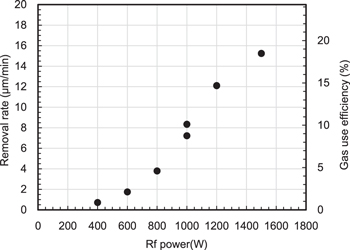
Figure 3. Removal rate dependence of 2-inch SiC wafer on rf power. The righthand axis depicts gas use efficiency.
Download figure:
Standard image High-resolution imageFrom the figure, it was discovered that the removal rate increased with an increase in the rf power and an extremely high removal rate of 15.2 μm min−1 (material removal rate of 30.8 mm3 min−1) was achieved at 1.5 kW. Here, approximately 18% of the supplied SF6 gas was consumed during the chemical reaction. Since there was a continual increase in the intensity of plasma emission as the input power increases, there was a corresponding increase in the radical density as the plasma density increased, thus, leading to an increased removal rate. The same tendencies were observed in our previous studies. 21,26,31 Additionally, since the removal rate of SiC by PCVM was known to be highly dependent on temperature, 31 an increase in the surface temperature of the substrate due to the increase in the rf power may also contribute to the increase in the removal rate. The temperature of the edge part of the wafer during 10 min experiments at the rf power of 0.6, 0.8 and 1.0 kW were measured using thermography from the top of the chamber by a special arrangement of shifting the electrode position, which resulted in the maximum temperature of 120 °C, 160 °C, and 200 °C, respectively. Extrapolating from these, it appears to be about 300 °C at 1.5 kW. Experiments with an rf power higher than 1.5 kW were not conducted because of the risk of cracks in the substrate and abnormal discharge. The removal rate is expected to further increase with a higher rf power source. For reference, the removal rate with 1.3 kW at 1.5 kPa, where the maximum removal rate was obtained in the SF6-pressure-dependence experiment, was approximately 12 μm min−1 which was almost the same as that at 2.5 kPa.
Processing gap dependency
The experiments for evaluating the removal rate dependence on the processing gap were conducted with a pressure of 2.5 kPa, rf power of 1 kW, SF6 flow rate of 400 sccm, and processing gap range of 0.75 to 3.0 mm. The results are illustrated in Fig. 4. A plasma was not generated and the experiments were not conducted in a gap wider than 3.0 mm and narrower than 0.75 mm. Figure 4 revealed that there is no significant correlation between the processing gap and the removal rate at gaps where the experiments were performed.
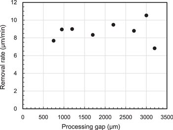
Figure 4. Relationship between the removal rate of 2-inch SiC wafer and the processing gap.
Download figure:
Standard image High-resolution imageIn the case of an RIE process, the energy of the ions has a significant impact on the removal rate, and the sample is usually subjected to a bias voltage. 22 Thus, the energy of the ions is ultimately determined by the bias voltage and is not depend on the distance between the electrode and samples. In the case of this study, because the etching is performed by neutral radicals rather than ions, the density of neutral radicals could be dependent on the distance between the electrode and samples, however the results were not. Similar results were also obtained in our previous study. 21 Generally, the electric field strength between the electrode and the sample is inversely proportional to the processing gap in the absence of plasma. However, once a plasma is generated, a thin ion sheath of a constant thickness is formed over the electrode and sample surfaces, and the potential gradient is almost zero in most of the spaces between the electrode and the sample. Thus, the effect of the processing gap length on the plasma density is considered to be minimal, which results in no-dependency of the removal rate on the processing gap.
Since it was discovered that the removal rate was independent of the processing gap changes on the order of mm, it can be deduced that keeping the processing gap constant by controlling vertical axis of the electrode is unnecessary even if the wafer thickness decreases on the order of sub-mm during the thinning process.
Dependency on SF6 gas flow rate
Figure 5 illustrates the experimental results of evaluating the removal rate dependence on the SF6 gas flow rate. The experiments were conducted with a pressure of 2.5 kPa, processing gap of 1.7 mm, rf power of 1 kW, and SF6 flow rate varied from 300 to 500 sccm. Although it was expected that the removal rate would increase with an increase in the supply of SF6, which is the source of the F-radical, the results, however, revealed a little removal rate dependence on the SF6 flow rate between 300 and 500 sccm, as depicted in Fig. 5. Since the removal rate is independent of the SF6 flow rate, the gas consumption efficiency decreased with an increase in the flow rate.

Figure 5. Dependence of 2-inch SiC wafer removal rate on SF6 flow rate. The black circles represent the removal rate and the diamond shapes denote the gas use efficiency (the righthand axis).
Download figure:
Standard image High-resolution imageGenerally, in plasma etching, the removal rate tends to increase as the gas supply is increased, 32–34 and such result was obtained in our previous studies. 21 However, it is almost constant in this experiment. In another experiment using SiC substrates, an exponential increase in removal rate has been found as the substrate temperature is increased by the heater, even when the plasma is generated at the same power. 31 In that case, although the F radicals are generated sufficiently by the plasma, the etching reaction itself seems to be limited by the substrate temperature. Since the temperature of the substrate was approximately constant in this experiment, the reason why the removal rate was constant is thought to be that the removal rate was limited by the substrate temperature not by the number of the F radicals. However, further studies such as the measurement of F radical density are needed in the future to clarify this phenomenon.
Dependency on wafer diameter
The rf power dependence on the removal rate of 3- and 4-inch wafers was investigated at a pressure of 2.5 kPa, processing gap of 1.7 mm, and SF6 flow rate of 400 sccm. The experiments were conducted by preparing scaled-up electrodes for each wafer diameter, and the experimental results are illustrated in Fig. 6 along with the result of a 2-inch wafer. As shown in Fig. 6, at the same power, the removal rate decreases as the wafer diameter increased, but the removal rate increases with increasing power at each diameter. For the 4-inch wafers, the removal rate of 6.4 μm min−1 and the material removal rate of 67.4 mm3 min−1 were achieved with an rf power of 3.2 kW, which is the highest material removal rate ever realized. Figure 7 shows the re-plotted data with the horizontal and vertical axes representing the rf power density (rf power per unit area) and removal rate, respectively. From the figure, it was discovered that almost the same removal rate was obtained with the same rf power density even with different wafer diameter. This indicates that, even for 6-inch wafers which are now the mainstream, a high removal rate of approximately 10 μm min−1 is expected to be achieved with an rf power of approximately 10 kW which can be output by a standard commercial rf power supply. Although such high-power rf power supply is a little bit expensive, since a PCVM thinning apparatus does not need an expensive high-vacuum pumping system required for an RIE equipment or a high-rigid frame required for a high-precision grinding machine, we think it would not be so expensive if it is mass-produced.

Figure 6. Dependence of removal rate of 2-inch (black circle), 3-inch (diamond shape), and 4-inch (black triangle) SiC wafers on rf power.
Download figure:
Standard image High-resolution image
Figure 7. Dependence of removal rate of 2-inch (black circle), 3-inch (diamond shape), and 4-inch (black triangle) SiC wafers on rf power density (rf power per unit area).
Download figure:
Standard image High-resolution imageThinning demonstration
Thinning of a commercially available 2-inch wafer to less than 100 μm was demonstrated. The pressure was set to 2.5 kPa, processing gap to 1.7 mm, rf power to 1 kW, SF6 flow rate to 400 sccm, and the processing was performed for about 20 min. The thickness distribution before and after processing was measured by a spectral interferometer (KEYENCE SI-F80R). The line profiles of the wafer thickness before and after processing are depicted in Fig. 8. Although the amount of machining at one end is small, it can be observed that the thickness of the wafer becomes roughly less than 100 μm after only 20 min of processing. Concerning the uniformity, the distribution of the removed thickness is relatively large (about 14%) and the distribution of the thinned thickness is almost 40% except the edge part, which should be improved for practical use. Since it is found that the removal profile distribution highly depends on the arrangement of location of the gas supply nozzles on the electrode, we optimize the arrangement near future.

Figure 8. Wafer thickness distributions before (dotted line) and after (solid line) 20 min thinning.
Download figure:
Standard image High-resolution image
In the thinned profile illustrated in Fig. 8, there were a few points where data was missing, which is because the thickness data could not be measured where etch pits exist. It should be emphasized that the surface where there was no etch pit maintained a mirror appearance. Although the surface roughness was not evaluated in this study because of existence of the etch pits, it has been found that a mirror surface with a surface roughness of approximately 0.3 nm rms (root mean square) can be obtained if no etch pits are generated. 27 It was reported that under high rf power conditions where the substrate temperature is high, etch pits are generated around the threading screw dislocations whose diameter and depth are several-ten μm and several-ten μm, respectively. 35 However, it was also reported that the etch pit once formed becomes reduced in size under the low rf power condition, and the combination of high and low rf power conditions enables thinning with suppressed etch pit formation.
Conclusions
A high-pressure SF6 plasma etching method was proposed for strain-free thinning of SiC wafers using SF6 plasma at approximately 2.5 kPa. It was noticed that the entire 2-inch wafer can be thinned at a high removal rate of 15 μm min−1 by increasing the rf power. The removal rate was discovered to be mainly dependent on the power density and relatively insensitive to processing parameters such as processing gap and gas flow rate. It was also discovered that almost the same removal rate can be achieved with an rf power proportional to the area of the wafer even if the wafer diameter is increased. It was demonstrated that the thickness of the commercially available 2-inch wafer can be thinned to approximately 100 μm by only 20 min plasma etching. In the present result, the thickness uniformity is not sufficient yet for practical use. However, it will be improved by optimization of the location of the gas supply nozzles on the electrode in the near future.
Although the high electric field for plasma generation may affect the device components on the frontside, since the processing is on the backside, the electric field was considered to be shielded by the low-resistance wafer itself. Though the shielding effect against the electric field may be weakened due to the thin substrate thickness, it would not amount to a severe defect because the devices on the frontside can withstand voltage of several hundred volts. On the other hand, deterioration of SiO2/SiC interfacial properties due to ultra–violet (UV) irradiation has also been reported. 36 Although the effect of UV light from the plasma is a concern, we think it is not serious because the amount of the UV light reaching from the backside to the frontside surface is very small due to very thin penetration depth of the UV light 37 ; however, we will carefully study the phenomenon in the future. The effect on the device structure of the front surface and methods to prevent from the reduction of wafer diameter by side-surface etching will also be studied in the future.
This method not only contributes to cost minimization owing to the reduction of the processing time and non-use of an expensive diamond wheel but also improves the reliability of the fabricated devices because it leaves no sub-surface damage on the backside of the wafer. The application of this method would result in a wider-spread utilization of low-power consumption SiC power devices toward a sustainable society.