
Abstract
Novel hybrid non-volatile memories made using an ultra-fast microwave heating method are reported for the first time. The devices, consisting of aligned ZnO nanorods embedded in poly (methyl methacrylate), require no forming step and exhibit reliable and reproducible bipolar resistive switching at low voltages and with low power usage. We attribute these properties to a combination of the high aspect ratio of the nanorods and the polymeric hybrid structure of the device. The extremely easy, fast and low-cost solution based method of fabrication makes possible the simple and quick production of cheap memory cells.
Export citation and abstract BibTeX RIS
1. Introduction
Since the first reported link [1] between resistive switching in nanoscale TiO2 devices from HP research labs and Leon Chua's theoretical description of memristors [2] resistive switching devices or memristors have gained considerable new interest. Considered now an emerging technology [3] they have been increasingly seen as candidates for new universal memories as they combine the high speed and high density typical of static random access memory (SRAM) and dynamic random access memory (DRAM) with the non-volatility typical of FLASH memories. Their highly scalable nature, allowing the positioning of memory cells at very high densities using simple crossbar architectures [4, 5], is also of central importance as a new era of technologies emerge to counter increased difficulties in retaining electrons in shrinking dimensions in conventional memories, as highlighted in a recent report [3] from the international technology road-map for semiconductors, which expects that 'SRAM and FLASH scaling in 2D will reach definite limits within the next several years'. Memristors are also increasingly seen as having important applications in neuoromorphic applications since they emulate the electronic and chemical actions of synapses [6], which are central to learning, memory and reasoning in biological systems as well as playing important roles in the registering of stimuli (touch, sound, light, smell), regulation of hormone levels and controlling muscles. Exploiting memristors in this manner to make neuromorphic computing architectures [7] has many important applications in visual and auditory perception, motor control, multisensory integration in automated systems (e.g. robotics), learning and artificial intelligence.
Much less-studied in the memristor field is the use of hybrid materials, those containing both organic and inorganic components. These materials have the potential for making a large impact because they combine the electronic properties of semiconductors with the solution processing advantages of organic materials i.e. low temperature processing and large area coverage at very low cost and on lightweight and flexible substrates. To date only a few papers have been reported on hybrid memristor devices containing inorganic semiconducting materials [8, 9] mixed with polymeric materials. In this article we report on the development of high quality hybrid memristor devices that are made using an extremely simple and ultra fast solution processing route based on a microwave oven. The hybrid devices consist of highly aligned vertical ZnO nanorods embedded in an insulating polymeric matrix, see figure 1. The ZnO nanorods are grown using an exceptionally quick microwave heating technique using an ordinary conventional microwave oven [10] and the polymer layer is deposited using a simple spin coating operation. We report on the room temperature I–V characteristics and switching properties of the devices. The results show the devices exhibit fast bi-polar switching operation with good data retention and ideally low operating voltage and power usage. Importantly, the devices do not need a forming step for initialization of the memory cell, a property considered highly important for commercialization since forming processes are generally complex, not well understood and because of their stochastic nature, result in widely varied behaviour.
2. Experimental section
The devices were fabricated and characterized using the following methods. Vertically aligned ZnO nanorods were grown on indium tin oxide (ITO) coated glass using a microwave heating process. A seeding technique, consisting of a 10 mM solution of zinc acetate dehydrate (98%, Aldrich) in 1-propanol (spectroscopic grade) was spin coated three successive times at 2000 rpm for 30 s to form nucleation sites for growth of the nanorods. Prior to spin coating the glass slides were cleaned by sonication in acetone and isopropanol for 10 min and dried in a nitrogen flow. Alignment of the nanorods was achieved by annealing the seeded slides on a hotplate at 350 °C for 30 min in air [11]. Growth of the nanorods was carried out using a microwave technique [10], and consisted of suspending the substrates upside down in a closed beaker containing an equimolar mixture of 25 mM zinc nitrate hexahydrate (Zn(NO3)2·6H2O, Sigma Aldrich) and hexamethylenetetramine (HMTA, Sigma Aldrich) in deionized (DI) water (resistivity 18 M Ω cm) and heating with a conventional microwave oven (2.45 GHz) at 900 W for 2 min. Homogenous heating is ensured by revolving the beaker at 5 rev min−1. Afterwards the devices were cleaned by rinsing in DI water with drying under nitrogen flow. Figure 1 (top right) shows a scanning electron microscopy (SEM) image of a typical ZnO nanorod thin-film. The length and diameter of the nanorods can be both varied depending on the heating time of microwave growth and temperature of the seed annealing step. The above conditions yielded nanorods that were approximately 500 nm in length with diameters of 40–50 nm. The polymer layer consists of spin-coating a poly(methyl methacrylate) (PMMA) solution (Sigma Aldrich, 120 000 MW, 3% by weight in toluene) at 2000 rpm for 60 s, typical resulting in a layer thickness of ∼100 nm. This was followed by annealing at 150 °C for 30 min to remove any unwanted solvent. Top contacts for the devices consisted of either Al or Au (100 nm thick), deposited by thermal evaporation under vacuum conditions through a mask containing 100 μm diameter circles. I–V characteristics and pulse measurements were carried out using a probe station equipped with an Agilent B2912A source-meter unit. All measurements were carried out at room temperature in ambient atmosphere.

Figure 1. Memristor device schematic showing the vertically aligned ZnO nanorods embedded within a polymer material (lower image) with aluminium (top) and bottom (ITO) electrodes. An ultra-fast fabrication technique using a conventional microwave oven (upper left) is used to make the aligned nanorods (upper right).
Download figure:
Standard image High-resolution image3. Results and discussion
Figure 1 (top right) shows a typical SEM image of the high quality ZnO nanorod layer grown by the microwave oven technique. The nanorods grow perpendicular to the substrate and exhibit excellent vertical alignment. X-ray diffraction measurements taken of the thin-films (not shown) indicate their structure is typical of well-ordered crystalline ZnO with a hexagonal wurtzite structure in the c-direction [12]. The fast microwave growth technique compared with other slower hydrothermal methods is expected to minimize structural defects caused by dissolution of the ZnO nanowires in the growth solution during growth. During growth a number of chemical reactions occur within the solution to from the ZnO nanowires ZnO. Initially the HMTA decomposes in the solution to form formaldehyde and ammonia. The ammonia reacts with the water in a hydroxyl supply reaction to produce NH4+ and OH− ions. A supersaturation reaction occurs with the Zn2+ ions from the zinc nitrate hexahydrate, forming Zn(OH)2. With heating, the Zn(OH)2 decomposes to ZnO and water [13].
Decomposition reaction:

Hydroxyl supply reaction:

Supersaturation reaction:

ZnO nanowire growth reaction:

Alignment and morphology of the nanowires during the growth step is primarily governed by the alignment, size and crystallinity of the seed layer [11, 13, 14]. The HMTA in the solution serves three main roles: it provides the OH− ions needed to initiate the hydroxyl reaction; it acts as a pH buffer within the solution, as the hydrolysis rate of HMTA is decreased by an increase in pH and vice versa; it also attaches to the non-polar facets of the nanowires during growth, preventing the access of Zn2+ ions to these facets and thereby leaving only the polar (001) face for epitaxial growth [13, 15]. The second of these roles is particularly important, as it is believed that high supersaturation levels favour nucleation while low supersaturation levels favour crystal growth [13, 16]. Rapid production of OH− ions within a short period causes Zn2+ ions to precipitate out quickly due to the high pH environment, minimizing the contribution of the Zn2+ ions to the nanowire growth and rapidly consuming the nutrient, resulting in the eventual prohibition of further growth of the nanowires [17]. The use of HMTA in the growth solution contributes to maintaining a low supersaturation level by controlling the concentration of OH− ions in the solution.
Figure 2(a) shows the current–voltage (I–V) characteristics of a typical ITO/ZnO–PMMA/Al memory cell when swept between −3 V and +3 V. The 'pinched hysteresis loop' in both positive and negative quadrants is a signature of bi-polar memristor behaviour. The red and black lines, having resistances of ∼1 kΩ and ∼10 kΩ, indicate the low resistance 'on' state (LRS) and high resistance 'off' state respectively. After fabrication the devices are in the high resistance off state. For a voltage sweep from zero to higher positive voltages the current in the device rapidly increases from about 0.75 V onwards, indicating transition to the low resistive state. The sweep from +3 V to −3 V shows the transition back to the high resistance state. In this case the gradient of the curve is linear and goes through the origin indicating the LRS is ohmic in nature. At approximately −1.5 V the device begins to revert back to the HRS. Figure 2(b) plots the same data but as current density versus electric field. The plot shows good symmetry between the two I–V curves and a wide separation between the two resistive states. Importantly, only very small electric field values are required for the switching, as shown by the maximum field values of 0.04 M V cm−1 and −0.04 M V cm−1. Devices were also measured in which Au top contacts were used instead of the Al ones discussed here. This had no significant effect to the above mentioned bipolar resistive switching operation.
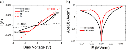
Figure 2. (a) Plot of the I–V characteristics for a typical hybrid device and showing the transitions between the low resistance ohmic (on) state (red) and the high resistance non-ohmic (off) state (black). (Note: arrows indicate direction of the sweep.) (b) Plot of the absolute current density versus electric field, showing the good separation of the states and the small electric field values for switching.
Download figure:
Standard image High-resolution imageInterestingly no forming step was needed to initialize the devices prior to obtaining the I–V curves. Figure 3 clarifies this further by showing the first three I–V sweeps on a pristine device. The graph indicates that at even smaller sweep voltages amplitudes (2.0 V), instead of the 3.0 V used in figure 2, the characteristic switching loop of a memristor is obtained without a forming step. Subsequent I–V sweeps also show no difference in shape or switching voltage, demonstrating the forming free operation of these devices.
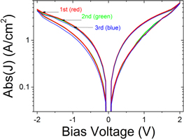
Figure 3. Plot of the absolute current density versus applied voltage for a pristine device, showing the characteristic switching loop of a memristor is obtained without a forming step. The first I–V sweep of the device has the same shape and switching voltage as subsequent sweeps indicating that no forming step had occurred during the first I–V sweep.
Download figure:
Standard image High-resolution imageThe pulse dependent switching behaviour for a series of 10 ms set and reset pulses at +3.0 V and −3.0 V respectively is shown in figure 4(a). Read pulses of 50 mV with duration of 10 ms were used between the set and reset pulses to monitor the resistance of the states. The corresponding current monitored during the read pulse of the cycle, shown in figure 4(b), clearly demonstrates repeatable switching between two distinct resistive states with an on/off resistance ratio of 2.5 and very good stability of both states over the length of the cycle.

Figure 4. Plots with the same time base for a series of (a) set, reset and read voltage pulses and their corresponding (b) read currents. Note: the read pulses in (a) are only just visible as they have only a small voltage (50 mV).
Download figure:
Standard image High-resolution imageThe effect of the polymer layer was investigated by comparing devices fabricated following the procedure above with devices that contain no PMMA layer. In this case the structure of the devices were ITO/ZnO nanorods/Al and the ZnO nanorods were grown using the same microwave method as that described in the paper. In figure 5(a) the I–V characteristics of a typical ZnO nanorod device containing no PMMA layer is shown. The device similarly shows resistive switching properties however there are notable differences to devices that contain a PMMA layer. One of the key differences is the devices are much less stable. The current typically shows abrupt, first-order changes in value during a single I–V sweep, often with transitions to intermediate quasi-stable states. The voltage at which transitions to the on and off states occurs also varies, often unsystematically and with no observable pattern upon successive sweeping, as shown in figure 6. The I–V curves are also very asymmetric in comparison to devices that contain a PMMA, most likely a reflection of the asymmetry of the two different semiconductor/metal interfaces. Another key difference is the currents are much larger in devices without a PMMA layer, typically by more than an order of magnitude. This is not particularly desirable for low power operation. These results suggest the PMMA layer plays an important role in the switching properties of the devices by acting to diminish the influence of the electrode. We speculate the insulating layer works by smoothing out the interface region and masking local effects at the electrodes, such as surface defects and surface roughness. The PMMA layer may also act to impede the formation of small filaments caused by the migration of the electrodes surface atoms, which could be responsible for the observed instabilities in the set/reset voltages for devices without a PMMA layer.
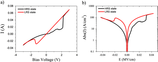
Figure 5. (a) Plot of the I–V characteristics for a ZnO nanorod device without a PMMA layer and showing the transitions between the low resistance ohmic on state (red) and the non-ohmic off state (black) states. (b) Same data plotted as absolute current density versus electric field.
Download figure:
Standard image High-resolution image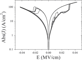
Figure 6. Current density versus electric field for a ZnO device containing no PMMA layer and showing unstable properties.
Download figure:
Standard image High-resolution image
In the following we discuss briefly the advantages of the hybrid devices, role of the nanorods and the mechanism that may responsible for their switching behaviour. We note that here we only report our very recent findings, highlighting instead the advantages of a solution based method for making memristors. More complete investigation of the switching mechanism, role of the PMMA and reasons why a forming step is not required is currently underway and will be reported in a later paper. As for now we only speculate on the role of the nanorods in the switching mechanism using our present results and that known from the literature.
In general it is well known that ZnO, along with other transition metal oxides show changes in their resistance depending on the applied voltage [18]. The mechanism of switching is still under considerable debate. Early measurements on doped ZnO thin films [19] showed bipolar switching regardless of the substrate, dopant species or microstructure of the samples. Later, in undoped TiN/ZnO/Pt devices [20] the switching was explained by the formation and rupture of filamentary conductive pathways with the generation/recovery of oxygen vacancies and non-lattice oxygen ions playing a critical role [21]. More recently in Ag/ZnO:Mn/Pt thin-film devices switching was found to be caused by the formation and rupture of Ag bridges mediated by redox reactions as evidenced by in situ TEM studies combined with EDX analysis [22].
In the case of hybrid ZnO devices there have only been a few reports. For ZnO nanoparticles blended in PMMA and sandwiched between Al and ITO contacts, the observed bi-polar resistive switching [8] was proposed to be due to a barrier type effect involving charging of the nanoparticles and the formation of an internal electric field. A ZnO nanorod/PMMA heterostructure [9] grown instead using a chemical-bath method [23] and with the seed layer deposited using RF sputtering was instead believed to be caused by the formation and rupture of conductive filaments due to the migration of ionized oxygen vacancies.
In contrast, our rather un-optimized devices show surprisingly good switching characteristics leading us to speculate the nanorods play a key role in the switching properties. The high aspect ratio of the nanorods we expect enhances the electric field between the ends of the nanorods and the top Al electrode of the device, leading to switching at small electric fields, even with a relatively thick dielectric layer present [24]. The nanorods, high surface area to volume ratio is also likely to be important since in transition metal oxides it is generally known that the mobility of defects at surfaces is much higher than in single crystals [25]. Thus it is possible that either oxygen vacancies and/or zinc interstitials confined on the surface of the ZnO shuttle up and down along the lengths of the nanorods to mediate the switching [26].
The organic material also plays a key role in the switching. Aside from isolating the top electrode from the nanorods and eliminating any potential short-circuits between the ITO and Al electrodes, we speculate the polymer acts to smooth out local effects of the electrodes, such as surface defects and surface roughness effects that can cause unpredictable device properties. In contrast to a previous report on ZnO nanorod devices that do not contain a polymer layer [27], our devices show similar on/off resistance ratios but more symmetrical I–V properties. We have also prepared devices without a polymer layer. Measurements on these devices show similar on/off resistance ratios to our devices with a PMMA layer but their I–V curves are asymmetrical and their electronic properties are unstable. The measurements typically show unpredictable changes in current during a single I–V sweep along with erratic changes in the set and reset voltages. Another surface effect that can be important for switching is the migration of surface atoms from the electrodes (typically Cu, Ag), as utilized in electrochemical metallization memory cells (including ZnO devices) [28]. Here we expect the presence of the 100 nm thick PMMA layer prevents Al atoms from migrating to form conductive filaments. Preliminary investigations by us with Au and Ni as top electrodes instead show no noticeable difference indicating the influence of the electrodes is diminished in these devices, possibly because of the incorporation of the PMMA layer.
4. Conclusions
In summary, we demonstrate a high performance hybrid polymer-nanorod memristor device that has been fabricated using an ultra-fast and simple solution processing technique based on a conventional microwave oven. The ZnO nanorod-polymer device exhibits reliable and reproducible bipolar resistive switching with the advantages of low set/reset voltages (<3 V), low power usage (∼9 mW) and good memory margin (ROFF/RON ∼ 10). Importantly the devices do not require a forming step for initiation, which is particularly advantageous as it eliminates an additional step in the manufacturing of commercial devices. We attribute these properties to the combined nanorod/polymeric structure of the device. The nanorod geometry we expect enhances the electric field between the ends of the nanorods and the top Al electrode of the device, leading to switching at small electric fields, while the PMMA layer likely acts to smooth out local effects of the electrodes, such as surface defects and surface roughness effects, leading to greater device stability. Aside from the deposition of the top metal electrode the entire fabrication method is based on simple and easy solution processing techniques. The ZnO nanorods are grown using an exceptionally quick microwave heating technique using an ordinary conventional microwave oven and the polymer layer is deposited using a simple spin coating operation. This extremely easy, low-cost and rapid fabrication method combined with low voltage/power operation should make possible the simple and quick production of cheap memory cells.