

Abstract
Scanning tunneling microscopy (STM) at 5 K is used to study WSe2 layers grown on epitaxial graphene which is formed on Si-terminated SiC(0 0 0 1). Specifically, a partial hydrogenation process is applied to intercalate hydrogen at the SiC–graphene interface, yielding areas of quasi-free-standing bilayer graphene coexisting with bare monolayer graphene. We find that an abrupt and structurally perfect homojunction (band-edge offset ~0.25 eV) is formed when WSe2 overgrows a lateral junction between adjacent monolayer and quasi-free-standing bilayer areas in the graphene. The band structure modulation in the WSe2 overlayer arises from the varying work function (electrostatic potential) of the graphene beneath. Scanning tunneling spectroscopy measurements reveal that this effect can be also utilized to create WSe2 quantum dots that confine either valence or conduction band states, in agreement with first-principles band structure calculations.
Export citation and abstract BibTeX RIS
Introduction
Two-dimensional (2D) transition metal dichalcogenides (TMDs) [1] are atomically thin semiconductors that have great potential for future electronic and optoelectronic devices [2, 3]. To achieve this, viable control of their electronic band structure is required to modulate charge carrier polarity [4–12] or facilitate low-resistance metal contacts [13, 14]. As yet, junctions based on these materials were realized by electrostatic gating [4, 11], and the fabrication of lateral [7–10] and vertical [8, 12] heterostructures. In addition, chemical doping [5, 6] was used to modify the majority carrier type and establish p-n diode characteristics.
In this Letter, we demonstrate an alternative path for creating lateral TMD homojunctions by utilizing patterned hydrogenation of the epitaxial graphene (EG) that the WSe2 layer resides on. Using a patterned template with coexisting areas of bare and hydrogenated graphene [15], we show that abrupt and structurally perfect homojunctions can be formed. These homojunctions do not form in the same manner as a conventional p-n junction—by carrier transfer from one side of the junction to the other, and concomitant production of space charge (from dopant cores) on the two sides of the junction. Rather, the effects observed here are fully explained in terms of the electrostatic potential of the underlying graphene, with this potential then superimposed on the WSe2 overlayer. We argue that this mechanism explains the lateral junction formation also in other related 2D heterostructure systems [16, 17] in which interlayer coupling is weak and gap states are absent. It is also shown that this approach enables one to create WSe2 quantum dots that confine either valence band (VB) or conduction band (CB) states, paving the way for tailoring TMD-based quantum materials.
Methods
Sample preparation
Prior to EG growth, the Si-terminated SiC(0 0 0 1) substrate was annealed at 1500 °C in a H2/Ar mixture (molecular weight ratio 1:4, 500 Torr) for 30 min to remove damaged material from the surface. Annealing at 1500 °C was then continued inside of a graphite-made crucible in 100% Ar atmosphere (700 Torr) for 15 min to form a nominal coverage of one monolayer of graphene on top of the carbon buffer [18]. Then, the reactor was cooled down to temperatures below 1000 °C at a rate of 30 °C min−1 and finally cooled down slowly to room temperature (RT). Subsequently, WSe2 was grown on graphene via a metal-organic chemical vapor deposition (MOCVD) process [19]. WSe2 growth was done at 800 °C in 100% H2 atmosphere (700 Torr) for 30 min. After the growth step, the tungsten precursor (W(CO)6) flux was stopped while the Se precursor (H2Se) flux continued for another 10 min to reduce Se-related vacancies and point defects in the WSe2 layer. The reactor was then cooled to RT at a rate of 50 °C min−1 in H2. Because the ambient conditions for WSe2 growth are nearly identical to those for hydrogen intercalation at the graphene–SiC interface [20], some of the carbon buffer beneath WSe2 was decoupled from SiC via H-intercalation, thus turning those areas into WSe2 residing on quasi-free-standing bilayer graphene (QF2L).
STM experiment
The STM measurements were performed in ultrahigh-vacuum (UHV) and at a temperature of 5 K. Electrochemically etched tungsten tips were cleaned by Ne ion sputtering and electron beam heating. After transfer under ambient conditions, the samples were annealed at 550 K in UHV and loaded into the microscope cooled down to 5 K. STM images were recorded in constant-current mode; bias voltages V refer to the sample with respect to the tip. Scanning tunneling spectroscopy measurements of the differential tunneling conductance dI/dV were carried out with lock-in technique (20 mV peak-to-peak modulation at a frequency of 675 Hz) to probe the local density of electronic states (DOS). We employ a variable-z measurement method in which an offset ΔS(V), which varies linearly with the magnitude of the sample bias, is applied to the tip-sample separation [21]. The exponential increase in conductance arising from this variation in tip-sample separation is then normalized by multiplying the data by a factor of e2κΔS(V), where κ is an experimentally determined decay constant of 1 Å−1 (averaged over bias voltage). This measurement method and subsequent normalization does not affect any detailed structure in the spectra, but it improves the dynamic range by one to two orders of magnitude. The noise level for the conductance is also measured, and normalization of that using the same method then yields a voltage-dependent noise level for each spectrum. Band edges are determined simply by the voltage (energy) at which the observed band-edge conductance intersects the noise level (or the observed conductance of the underlying graphene layer). A correction to those values is made in order to account for the modulation voltage [22], which produces an upwards (downwards) shift of the valence (conduction) band edge, by an amount equal to the peak amplitude of the modulation. Hence, with the correction, the band gaps are 20 mV larger than that given directly from the difference between observed band edge energies.
Theoretical calculations
The density functional theory (DFT) calculations were performed with the Vienna ab initio simulation package (VASP) [23]. The valence electronic states were expanded in a set of periodic plane waves, and the interaction between ions and the valence electrons implemented through the projector-augmented wave (PAW) approach [23]. The Perdew–Burke–Ernzerhof (PBE) generalized gradient approximation (GGA) exchange correlation functional was applied in the calculations [24]. The wave functions were expanded in plane waves with a kinetic energy cut-off of 500 eV. The convergence criteria for the electronic energy and ionic force relaxations are 10−4 eV and 0.01 eV Å−1, respectively. Integration over the first Brillouin zone was performed with a Γ-centered 24 × 24 × 1 k-point mesh. A vacuum layer over 20 Å was added to the direction normal to the monolayer and bilayer. During the ionic relaxation, the Grimme method was employed to describe the van der Waals interactions [25]. Spin polarization and spin-orbital coupling were applied in the electronic calculations.
Results and discussion
We used cryogenic STM at 5 K to study the MOCVD-grown WSe2 layers on EG which was formed on SiC. As described in the preceding section, a subsequent hydrogenation process was applied to intercalate hydrogen at the SiC–graphene interface and convert the initial monolayer (1L) graphene plus carbon buffer to QF2L [20]. We performed this treatment in a way such that only partial hydrogenation occurred, that is, the graphene substrate consisted of QF2L areas coexisting with 1L areas [26]. On such patterned graphene, WSe2 forms a continuous layer by overgrowing steps between adjacent QF2L and 1L areas. This is evident from the STM image in figure 1(a) showing QF2L islands overgrown by a single layer (SL) of WSe2. STM imaging at atomic resolution (figure 1(b)) reveals the hexagonal atomic arrangement within the topmost Se sheet and also shows that the lateral order remains unaffected by the graphene step beneath.
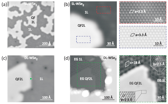
Figure 1. WSe2 growth on graphene with mono and bilayer terraces: (a) STM image (0.1 nA, 2 V) of single-layer (SL) WSe2 grown on epitaxial graphene (EG) consisting of monolayer (1L) and quasi-free-standing bilayer (QF2L) regions. (b) STM image (0.1 nA, −1.5 V) of SL-WSe2 overgrowing a 1L-QF2L step; close-up views (right) reveal the hexagonal arrangement (lattice constant a = 3.3 Å) in the topmost Se atom sheet of WSe2 on the upper (QF2L) and lower (1L) EG terrace. (c) STM image (0.1 nA, 2 V) of double layer (DL) WSe2 on 1L and QF2L EG. (d) Same as (c) after locally desorbing the WSe2 layer and exposing bare EG by applying a voltage pulse of 4 V to the STM tip held at constant height at the position marked in (c). In close-up view (right panel, 1 nA, 50 mV) the 1L region is identified by the honeycomb structure of graphene (b = 2.5 Å) and the 6 × 6 reconstructed SiC interface underneath (c = 18 Å), whereas the QF2L region appears as a flat terrace with the graphene atomic lattice corrugation.
Download figure:
Standard image High-resolution imageTo verify that the underlying graphene substrate consists of 1L and QF2L areas, we used the STM tip to remove the WSe2 layer in the vicinity of a step. Working on a surface area that had a continuous coverage of two layers of WSe2 (double layer, DL), the tip was held at constant height z at the lateral position marked in figure 1(c) and a voltage pulse of 4 V applied (figure 1 in the supplementary information (SI) (stacks.iop.org/TDM/6/021001/mmedia)). Figure 1(d) demonstrates that this treatment locally desorbs the WSe2 layer, leaving behind the bare graphene substrate with a step structure that appears to be the footprint of the initial WSe2 surface topography (figure 1(c)). In line with previous work [27–29], STM imaging of 1L graphene at low sample bias (figure 1(d), right panel) reveals the honeycomb structure of graphene together with the 6 × 6 reconstruction of the SiC buffer beneath. The corrugation of this reconstruction is absent on the QF2L area since there the buffer was converted to graphene by hydrogen intercalation [20]. The tip-induced desorption procedure used here is highly reproducible, allowing us to create defined pits in the WSe2 overlayer along with atomically clean and intact graphene at the bottom.
The underlying substrate modifies the electronic properties of the WSe2 overlayer. To quantify this, we measured the local DOS by recording the conductance dI/dV as a function of the sample bias V. We start the discussion with SL-WSe2 covering adjacent 1L and QF2L, see the STM image in the upper panel of figure 2(a). The corresponding conductance spectrum acquired on the 1L region (red curve in figure 2(b)) indicates a bandgap of 2.05 eV between the CB and VB edges, along with VB states ~0.7 eV below the VB edge (statistical average over various independent measurements yields a bandgap of 2.00 ± 0.06 eV). These observations are consistent with prior work [22, 30] which assigned the CB edge (denoted CBM) to a combination of valleys at the Q and K points, the VB edge to a valley at the K point (KV), and the next lowest VB edge arising from a local VB maximum (ΓV) at the Γ point of the surface Brillouin zone. The spectrum acquired on the QF2L region (blue curve) exhibits the same spectral features, but shifted ~0.25 eV higher in energy, suggesting a rigid upward shift of the WSe2 bands when moving from 1L to QF2L. For the DL-WSe2 case shown in the lower panel of figure 2(a), the corresponding spectra (orange and green curves in figure 2(b)) corroborate the expected trend of a reduced bandgap of 1.83 eV (statistical average 1.85 ± 0.04 eV) and a VB splitting (ΓV1 and ΓV2) due to interlayer coupling [30]. Nonetheless, also here a rigid energy shift of somewhat smaller magnitude is found between spectra taken at the two different graphene areas.
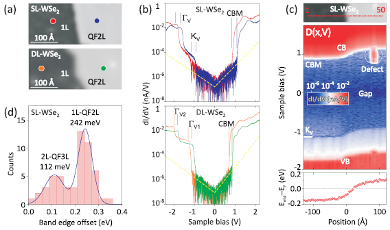
Figure 2. Lateral homojunction formation within the uniform WSe2 layer: (a) STM images (0.1 nA, 2 V) of a 1L-QF2L junction in SL-WSe2 (upper panel) and DL-WSe2 (lower panel). (b) Conductance spectra of SL (upper panel) and DL-WSe2 (lower panel) recorded at the tip positions indicated in (a). In both cases, spectra taken on the QF2L terrace are shifted to higher energy compared to spectra taken on the 1L terrace (see main text for discussion of respective spectral features); dashed lines indicate the noise level of the measurement. (c) DOS bias map D(x,V) (center panel) generated from fifty dI/dV spectra recorded along the line indicated in the upper panel. A uniform band edge shift to higher energy is observed as the lateral position is changed across the junction from 1L to QF2L EG. The in-gap state below the CB edge (marked by a circle) is induced by a point defect. The lower panel shows the variation of the mid-gap energy across the junction. (d) Histogram of band-edge offset values ΔE measured for various different junctions involving SL WSe2 layers. The main (side) maximum at 242 meV (1 1 2 meV) is associated with 1L-QF2L (2L-QF3L) junctions.
Download figure:
Standard image High-resolution imageTo further explore this behavior, we recorded a series of consecutive SL-WSe2 spectra along a line spanning adjacent 1L and QF2L regions. The resulting DOS bias map (figure 2(c), center panel) demonstrates the formation of a lateral homojunction within the continuous WSe2 layer. A uniform band-edge shift to higher energy is observed as the lateral position is changed from monolayer to free-standing bilayer graphene. The band edge offset ΔE deduced from the data in figure 2(c) is 0.24 eV. A statistical analysis of ΔE values determined from various different SL-WSe2 junctions yields the histogram shown in figure 2(d). Clearly, besides the main maximum at 242 meV—identified as the band-edge offset of WSe2 overlying a 1L-QF2L graphene junction as discussed before—there is a second maximum at 112 meV. We attribute this smaller ΔE value to junctions formed between adjacent bilayer (2L) and quasi-freestanding triple layer (QF3L) regions of the graphene substrate (figures 2(a) and (b) in the SI). Their existence on our samples is plausible because 2L areas formed during the initial graphene growth—which are likely to be present at small quantity even at a nominal coverage of one monolayer—will lead to 2L-QF3L junctions upon partial hydrogenation (since the buffer-layer carbon is converted to a new graphene layer upon hydrogenation).
Turning back to figure 2(c), the lower panel shows the variation of the mid-gap energy Emid across the junction. Within the picture of a conventional p-n junction, the data would suggest electron-doped WSe2 on 1L graphene and hole-doped character on QF2L graphene, with negligibly small doping concentrations due to the ~1 eV gap between the Fermi energy (at 0 V) and the respective band edges. At the same time, the junction is remarkably abrupt, showing a width of only ~100 Å. Clearly, this is incompatible with the picture of a conventional p-n junction for which the width of the space charge region is inverse to the carrier concentration [31].
We now discuss the origin of the lateral homojunction formation which cannot be explained by carrier depletion in a p-n junction as discussed above. Previous work has demonstrated that metal–semiconductor junctions formed by van der Waals interactions between TMDs and graphene exhibit negligible Fermi level pinning due to the absence of gap states [13, 16, 32]. Hence, a TMD layer on top of a junction formed in the graphene is expected to display a band-edge profile in the TMD that simply follows the potential profile in the graphene junction. For our experiments, EG on SiC is known to exhibit n-type character due to donorlike dangling-bond states existing at the SiC–graphene interface [15, 33, 34]. On the other hand, hydrogen-intercalated quasi-free-standing graphene has p-type character because of (i) the saturation of the dangling-bond states and (ii) the spontaneous polarization of hexagonal SiC(0 0 0 1) [15]. The carrier densities of the 1L and QF2L graphene are relatively high [33], thereby enabling an abrupt, lateral junction to form between them. Taking their vacuum levels (Evac) as initially aligned, then within the Schottky Mott rule electrons will transfer from one material to the other until Fermi level alignment is reached. A barrier is formed in the lateral junction with height given by the work function difference between QF2L and 1L graphene, ΔE  ΦQF2L − Φ1L, as illustrated in figure 3. Similarly, for the junction between 2L and QF3L graphene, a junction will form with barrier height of ΔE
  ΦQF3L − Φ2L. Now let us consider placing WSe2 (SL or DL) on these 1L-QF2L or 2L-QF3L junctions. Neglecting any charge transfer between WSe2 and graphene, then the WSe2 bands will simply align to the laterally varying graphene band structure, i.e. with some fixed offset ΔEC (ΔEV) between the WSe2 conduction (valence) band edge and the Dirac point of the graphene (as determined by
  the electron affinity of WSe2, ~3.55 eV [35]). Hence, in this approximation, we expect the same barrier height in the WSe2 lateral junctions as in the underlying graphene junctions [16]. We note at this point that the effect observed here is similar to the previously reported case of potential imprinting by charge impurities in graphene-boron nitride heterostructures [36, 37].

Figure 3. Schematic of WSe2 homojunction formed atop a 1L-QF2L EG junction: (a) Schematic band diagrams of 1L EG and SL-WSe2 in contact. The 1L EG is n-type due to electron transfer doping from the interface state associated with the buffer layer. WSe2 bands are aligned with the 1L EG in accordance to the CB offset, ΔEC. (b) Cross-sectional schematic of monolayer WSe2 (purple curve) grown on adjacent QF2L (double black curves) and 1L (single black curve) EG regions of the substrate. The buffer layer is closely attached to the SiC surface via chemical bonds (grey dots), with some dangling bonds (blue dots) exiting there. The SiC surface underneath QF2L is saturated by H atoms (green ellipses). (c) Band diagram corresponding to (b), indicating the varying band positions of the WSe2 across the junction; the WSe2 is slightly n-type (p-type) above the 1L EG (QF2L EG). A lateral homojunction thus forms in the WSe2 layer.
Download figure:
Standard image High-resolution imageUsing reported graphene work function values [33], one thus expects barrier heights for the 1L-QF2L and 2L-QF3L junctions of 0.55 and 0.33 eV, respectively. It is apparent that these values exceed the experimental result in figure 2(d) by more than a factor of two. However, it is known that for the 800 °C preparation conditions of our samples, a small amount of partial hydrogenation can occur even on the surface areas that are nominally pristine 1L or 2L graphene [38, 39]. That is, not only do areas of both pristine graphene and quasi-free-standing graphene occur over the surface, but also, the nominally pristine graphene is partially hydrogenated. We tentatively attribute our reduced barrier heights to this effect, since other possible charge transfer effects between graphene and WSe2 are expected to be relatively small (in-gap interface states are found to be absent at the graphene–WSe2 interface [16], defect densities in the WSe2 are low enough such that they would produce electrostatic potential shifts of 1–10 meV at most [40], and short-range interface dipoles [41] between WSe2 and graphene are not expected to vary across the 1L-QF2L or 2L-QF3L junctions since the topmost graphene layer is chemically unchanged across the junctions).
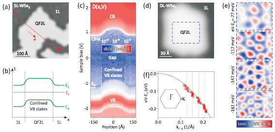
The lateral junctions of the graphene can be utilized to confine VB and CB states within the TMD layer. Consider, for example, the surface area overgrown by a SL-WSe2 layer as shown in figure 4(a): following the preceding discussion, along the dotted line in figure 4(a) one expects a spatial variation of the band-edge energies as sketched in figure 4(b). The corresponding DOS bias map (figure 4(c)) measured along the dotted line reveals the resulting band-edge modulation and suggests that states near the VB edge will be confined to the QF2L region. Consistent with this expectation, interference patterns of electron waves backscattered [42] at graphene steps are observed when probing states near the VB edge (figure 3 in the SI).
Figure 4. Quantum confinement in bilayer graphene islands overgrown by WSe2. (a) STM image (0.1 nA, −2 V) of an extended QF2L island overgrown by SL-WSe2; the dotted line defines a 1L-QF2L-1L junction. (b) Spatial variation of band-edge energies EV and EC as expected for the 1L-QF2L-1L junction based on the model in figure 3. (c) DOS bias map D(x,V) generated from fifty dI/dV spectra taken along the line in (a), corroborating the band-edge modulation sketched in (b). (d) STM image (0.1 nA, −1.3 V) of a compact QF2L island overgrown by DL-WSe2. (e) Spatial DOS maps D(x,y) recorded within the area marked in (d) reveal the lobe structure of VB states confined to the island; eV–EV is the energy relative to the VB maximum. (f) Wave vector kΓ–K versus energy (red dots) extracted from DOS maps as in (e) revealing wave vector quantization due to confinement; experimental data agree well with the DFT-calculated VB dispersion (green line).
Download figure:
Standard image High-resolution image
Confinement in sufficiently small islands leads to a measurable discretization of electronic states, thus establishing the formation of a TMD quantum dot [43]. Figure 4(d) shows such a case of a compact QF2L island overgrown by a DL-WSe2 layer. To visualize the nodal structure of the confined states, spatial DOS maps were recorded (figure 4(e)) showing quasi-hexagonal wave patterns due to the regular shape of the dot. Fourier transform power spectra of these spatial DOS maps yield peaked wave vector components along the Γ–K direction of the surface Brillouin zone (figure 4 in the SI); they are plotted versus energy in figure 4(f). The experimental kΓ–K values agree well with the VB dispersion (green line) calculated within DFT (figure 5 in the SI). In addition, the data points in figure 4(f) indicate that the confinement imposes wave vector quantization with a mean Δk value of 0.027 Å−1, see figure 4 in the SI. Given the boundary condition kn = nπ/L for confinement, with n an integer and L the dimension of the confining potential, we find L = π/Δk  116 Å which fits well with the size of the dot shown in figure 4(d). Conversely to the VB state confinement in figure 4, we find that CB states are confined in overgrown 1L patches embedded in QF2L regions (figure 6 in the SI).
Conclusions
In summary, the band-edge energies of an atomically thin TMD overlayer can be precisely modulated by lateral junction formation in a weakly coupled graphene layer, allowing one to create structurally perfect homojunctions of small lateral size and free of gap states. The modulation arises from the varying surface potential across the graphene which is directly superimposed as a bulk potential in the overlying TMD. We argue that this mechanism also explains the band-edge modulation recently observed in WSe2, MoSe2, and Te layers on graphene of varying thickness [16, 17]. The lateral junction formation that occurs in the 2D system studied here (and likely in other systems in which interlayer coupling is weak and gap states are absent [13]) is qualitatively different to what occurs in conventional p-n junctions, the latter implying carrier transfer and the production of a space charge region. It is anticipated that the 2D junctions studied in our work could be utilized for lateral carrier transport by adding a h-BN spacer between the graphene template and the TMD overlayer. Given the use of hydrogenated graphene, possibly electron beam lithography [44] could be employed to selectively desorb the hydrogen, thus writing a surface pattern that would be superimposed as a potential pattern in the 2D layer on top. This would represent a versatile approach to spatially modulate carriers in two dimensions, providing a test ground for fundamental research on quantum-confined electrons and a TMD-based material platform for 2D electronic circuits.
Acknowledgments
Y Pan and S Fölsch acknowledge financial support by the Deutsche Forschungsgemeinschaft (SFB 658). Y Pan also acknowledges the support from the National Key R&D Program of China (2017YFA0206202) and the National Science Foundation of China (11704303). Y-C Lin, B Jariwala, J A Robinson, and R M Feenstra acknowledge the support from the Center for Low Energy Systems Technology (LEAST). LEAST is one of six Semiconductor Research STARnet centers sponsored by MARCO and DARPA. Y Nie and K Cho were also supported in part by ASCENT, one of six centers in JUMP, a SRC program sponsored by DARPA.