
Abstract
We demonstrate the direct transfer of graphene from Cu foil to rigid and flexible substrates, such as glass and PET, using as an intermediate layer a thin film of polyimide (PI) mixed with an aminosilane (3-aminopropyltrimethoxysilane) or only PI, respectively. While the dry removal of graphene by an adhesive has been previously demonstrated—being removed from graphite by scotch tape or from a Cu foil by thick epoxy (~20 µm) on Si—our work is the first step towards making a substrate ready for device fabrication using the polymer-free technique. Our approach leads to an article that is transparent, thermally stable—up to 350 °C—and free of polymer residues on the device side of the graphene, which is contrary to the case of the standard wet-transfer process using PMMA. Also, in addition to previous novelty, our technique is fast and easier by using current industrial technology—a hot press and a laminator—with Cu recycling by its mechanical peel-off; it provides high interfacial stability in aqueous media and it is not restricted to a specific material—polyimide and polyamic acids can be used. All the previous reasons demonstrate a feasible process that enables device fabrication.
Export citation and abstract BibTeX RIS

Original content from this work may be used under the terms of the Creative Commons Attribution 3.0 licence. Any further distribution of this work must maintain attribution to the author(s) and the title of the work, journal citation and DOI.
1. Introduction
Graphene, a 2D monolayer of sp2-bonded carbon atoms, has been attracting great interest following its isolation by the mechanical cleavage of graphite [1]. Its unique physical properties, such as high intrinsic carrier mobility, tunable band gap, high mechanical strength and elasticity, and superior thermal conductivity, make graphene promising for many applications, such as high-speed transistors, energy/thermal management and chemical/biological sensors. As the current generation of silicon-based devices will reach their fundamental minimum size limit in the coming years, graphene provides an opportunity to enable even smaller devices [2].
Since graphene was isolated for the first time by the mechanical exfoliation method [1], different techniques have been developed for its production. Chemical vapor deposition (CVD) is the most promising due to the economic viability of its implementation for large-scale production. Graphene is typically obtained by CVD using different transition metal catalysts [3] to decompose hydrocarbon gas [4–7]. The two most commonly employed catalysts are Cu and Ni, each operating via a different mechanism depending on carbon precursor solubility in the catalyst. Cu has been demonstrated to grow monolayer graphene as carbon atoms adsorb onto the catalyst surface, forming single layer graphene sheets. Several studies have confirmed the growth of high quality graphene on single crystal Cu wafers and foils. Specially [1 1 1], and [1 1 0] orientations produced the highest quality due to the small lattice mismatch between graphene and Cu [8–10]. However, the elevated cost associated with wafers is a big challenge for the industrialization of such a technique. Because of this issue, cheaper polycrystalline Cu foils have become the standard catalyst for growing graphene. Several groups have demonstrated how proper conditioning of the Cu foil is crucial for improving graphene quality [9, 11, 12]. For example, precondition steps including cleaning and annealing, modifying roughness, crystallinity and grain size of the Cu surface, have been demonstrated to improve the electrical properties of the transferred graphene.
For the outstanding properties of graphene to be fully utilized, it must be transferable to a wide variety of substrates. Several methods have been developed toward this goal. The most commonly used method relies on a polymer-assisted transfer process. In this approach, usually known as 'wet-transfer', a polymeric layer (typically poly(methyl methacrylate), PMMA) [13–15] or a thermal release tape (TRT) [16] is used as a temporary substrate. On the one hand, PMMA and TRT are cheap, versatile and have good mechanical properties. On the other hand, since PMMA and TRT are in direct contact with graphene they leave residue upon removal. The residue poses a significant challenge as it has detrimental effect on graphene's electrical and mechanical properties [17–19]. An additional thermal annealing step in controlled atmosphere is often included to reduce the contamination level [11, 12, 20]. However, annealing does not fully remove contaminants and there is risk of degrading the graphene if the temperature is too high. Another approach to avoid the contamination issue is to grow graphene directly on the target substrate [21, 22]. Thus, the transfer step is avoided, reducing both processing steps and polymer residue. However, graphene grown directly on dielectric substrates, such as glass, is of rather poor quality compared to that on Cu [21, 22]. There are two additional promising solutions. The first one is known as 'hydrophobic transfer' [23], where Cu/graphene is slightly pressed to a substrate that has a surface hydrophobic coating. Since graphene is also intrinsically hydrophobic, it remains attached to the substrate during the etching of Cu in polar liquid. The second technique is known as 'dry-transfer' of graphene, which consists on the direct transfer of graphene from the Cu to the target substrate with the advantage of Cu recycling for future growth catalyst. Yoon et al [24] demonstrated for the first time the mechanical peeling of graphene from Cu with the calculation of the adhesion energies between graphene and Cu. Na et al [25] continued the study using a similar custom set up with the optimization of the separation speed to transfer a graphene layer of good quality and avoiding cracks. To this aim, graphene was peeled from Cu when located between two Si slides covered with epoxy adhesives of approximately 20 µm thickness and low thermal resistance. A more recent example has been the peeling off graphene from Cu using a flexible, lightness and chemical stable material such as polyimide (PI), where the adhesion strength between suitably cured PI-graphene is higher than that between graphene-Cu which makes possible the graphene detachment [26]. Further examples include the use of UV light for graphene transfer to an ultraviolet adhesive on PET [27, 28], and the transfer of graphene between two polymeric films using a hot press [29].
In the present work, we propose the direct transfer of graphene from Cu to glass and PET using PI as an intermediate layer between graphene and the target substrates. This is achieved by exploiting the high adhesion energies between graphene-PET, graphene-surface modified glass, as well as that between PI-graphene. For the process to be successful on glass, an adhesion promoter (3-aminopropyltrimethoxysilane, APTMS) was added to the PI precursor solution, increasing glass-PI adhesion. Our technique, if compared to the previous existing work, is the first step towards making a substrate ready for device fabrication. The use of a thin PI layer as an intermediate adhesive layer leads to an article that is transparent, thermally stable (350 °C) and free of polymer residue—such as PMMA for the wet transfer method- on the device side of the graphene. Also, our technique is faster than previous techniques with a reduction of curing times, easier as we use current industrial technology—a hot press and a laminator, and demonstrates a high interfacial stability in aqueous media. Also, although our work is based on a specific PI—VTEC—we also provide initial results using polyamic acid (PAA), thus demonstrating that our technique is not limited to an only specific material. The achievement of all previous statements demonstrates a feasible process that enables device fabrication. Further information can be found in tables S1 and S2 (supplementary information (stacks.iop.org/TDM/5/035022/mmedia)), where it is explained in detail, respectively, the main differences between our technique and previous dry and wet transfer methods.
2. Experimental section
2.1. Graphene on Cu foil
Graphene was grown on a smooth Cu foil of 18 µm thickness (Taiwan Copper Foil Co. LTD) using CVD (Black Magic 4 inch, AIXTRON) under the following conditions: CH4:H2 (1:4), 25 mbar and 10 min. Prior to graphene growth, Cu foil was first cleaned by rinsing in organic solvents and DI water (acetone: isopropyl alcohol: H2O, 2 min each), and finally in 0.1M aqueous acetic acid (CH3COOH) for 2 min to remove oxides from the Cu surface. Then, Cu foil was placed inside the CVD chamber and heated at 50 °C min−1 from room temperature to 1000 °C under an Ar/H2 flow. Graphene transferred from this Cu foil will be referred as 'Gr 1'. Also, commercial graphene was used for the laminator technique (Graphenea, 25 µm foil), which will be referred as 'Gr 2'.
2.2. Polyimide
PI VTEC-080-051, (Richard Blaine International, Inc. (RBI, Inc.)) was received as a solution of the PAA precursor in N-methyl-2-pyrrolidone (NMP). The specific structure for the VTEC polymer is RBI, Inc. proprietary information. Further experiments have been performed using other PAA precursors (PAA-431176 from Sigma Aldrich).
2.3. PI deposition on target substrates
The target substrates were Corning® EAGLE XG® glass (Corning Incorporated) and PET slides (Goodfellow Inc., of 125 µm thickness), both 2 × 2 inch in dimension. The substrates were cleaned using acetone and isopropyl alcohol, followed by O2/Ar (50:50) plasma cleaning at 50 W for 3 min. Cleanliness of glass was checked with contact angle measurements, assuming good cleaning for contact angles below 5°. A mixture of VTEC-080-051 and 3-aminopropyltrimethoxysilane, (APTMS), mAPTMS = 0.5%wt. × mPI or as received VTEC-080-051 was spin coated at room temperature at 3000 rpm, 1 min, on the glass or the PET, respectively. After spin coating, samples were pre-dried in an oven at 40 °C–80 °C for 15 min.
2.4. Graphene transfer
Two equipment have been used for the graphene transfer to demonstrate the feasibility of scale-up and of roll-to-roll processing:
- (a)Hot Press: Graphene transfer to glass was performed using an industrial hot press (WABASH MPI, GENESIS Hydraulic 30 TON PRESS) at 150 °C. Pressure (P(HP)) was increased from 25 to 350 psi with optimized values above 150 psi. During the transfer step, samples were under temperature and pressure for 10 min. In order to achieve a constant P(HP) distribution over the whole area, a silicone rubber sheet was placed on top of the sample.
- (b)Laminator: Graphene transfer to glass and PET was performed using a commercial laminator to simulate a roll to roll process (Catena 65, GBC). Pressure was modified by changing the distance (Δx) of the silicone rollers. During the transfer step, samples were introduced several times at low speed between the silicone rollers (optimum number of cycles = 12 and 6 for glass and PET, respectively). The optimized parameters for the laminator conditions were: Tc = 140 °C, Δx = 1–2 mm (glass) and 38 µm–1 mm (PET).
2.5. Characterization techniques
Surface analysis of transferred samples and glass substrates was realized by Atomic Force Microscopy (AFM, Bruker/Veeco Dimension 3100), FEI-scanning electron microscopy (FE-SEM, FEI Inspect F) and contact angle goniometric measurements (DSA100, KRÜSS). Chemical reactions of PI films were monitored by FTIR spectroscopy (BRUKER) at different temperatures to follow the curing process. Additional characterization comprised spectroscopic measurements (PerkinElmer Lambda 950 spectrometer) and micro-Raman analysis (InVia Renishaw, 532 nm laser excitation and 50× lens). The quality of the transferred graphene was checked by measuring graphene sheet resistance (Rs), carrier density (nS) and mobility (µH). Rs was measured using a 4-point probe equipment, while Hall measurements were performed to determine nS by a custom set-up (measurements and set-up are fully explained in the supplementary information, figures S1(a) and (b)). Flexibility tests were performed using a two-point bend testing setup connected to a motor driven by an electronic controller, allowing the arm to move back and forth along the horizontal direction. Graphene transferred to PET/PI samples were subjected to continuous bending. Rs was measured after each bending cycle while the bending radius was varied from 2 cm to 7 mm.
3. Results and discussion
At first, PI films were deposited on Cu/graphene following the procedure described in [26], and were characterized at different curing temperatures (Tc). Rs was chosen as an indicator to optimize the process by identifying the Tc at which graphene transfer occurs reliably. Figure S2(a) shows the most successful transfer of graphene to PI for Tc between 90 °C–130 °C. At 180 °C, Rs values oscillated from 6 kΩ sq.−1 values until MΩ, denoting poorer graphene adhesion or graphene damage. For further understanding of results, we characterized the PI films at different Tc, using weight loss (figure S2(b)) and FTIR (figure S3).
The initial precursor polymer solution contains VTEC in its PAA form which produces imides as it cures. The imidization progression of that PAA is a function of Tc and was followed by monitoring the increase/decrease of imide and amide IR absorption bands at: 1380, 1724 and 1774 cm−1, and 1530 and 1650 cm−1, respectively [30, 31]. At 80 °C–100 °C, there was minimal to no absorption band of the imide group (at 1774 cm−1, C=O asymmetrical stretching and 1380 cm−1, C–N stretching), which means that PAA remains the main component of the film. From 100 °C to 180 °C, conversion of PAA to PI starts to occur, which is confirmed by FTIR as imide peaks increase with temperature while the amide peaks decrease. Finally, after 250 °C PI was fully cured (all PAA was converted to PI) as revealed by the intense imide FTIR peaks together with the maximum weight loss of the film (87% weight loss after 250 °C). In accordance with these data, we hypothesized that Rs oscillation at 180 °C might be due to variability in the degree of imidization and that the failure to transfer graphene at Tc ⩾ 180 °C might be due to PI lacking carboxylic groups that could interact with graphene. This hypothesis can be confirmed by the disappearance above 180 °C of the FTIR peak at 1410 cm−1 related to carboxylic groups. This topic is currently under further investigation evaluating the robustness of the transfer process using other commercially available PAAs. Although all the data in this work are based on VTEC, the process has been demonstrated to work for other PAA precursors (PAA-431176 from Sigma Aldrich) obtaining comparable values of graphene coverage and Rs.
Besides Tc, we realized that two additional parameters P(HP) and Δx, which are related to the two equipment used for the graphene transfer, are fundamental to improving graphene quality.
The transfer procedure involves four main steps (figure 1): (1) the spin-coating of VTEC-APTMS or as-received VTEC on glass or PET respectively; (2) the PI drying at 40 °C–80 °C for 15 min to remove volatiles; (3) graphene transfer by locating Cu/graphene on top of the sample with the graphene face in direct contact to PI. The transfer was performed at Tc applying pressure with a hot press, P(HP), or a laminator (modifying the distance (Δx) of the silicone rolls). In order to achieve a constant P(HP) distribution over the whole area, we placed a silicone rubber sheet on top of the sample. The optimized parameters for the hot press were Tc = 150 °C, P(HP) = 150–300 psi for 10 min, while for the laminator optimal conditions were: Tc = 140 °C, Δx = 1–2 mm (glass) and 38 µm–1 mm (PET); (4) Cu was peeled-off leaving graphene attached to the (substrate/(APTMS+)PI) structure.

Figure 1. Graphene transfer to glass and PET using PI as an intermediate layer: (1) spin-coating of (0.5% APTMS + PI) at 3000 rpm, 1 min; (2) drying of (0.5% APTMS + PI) at 40 °C–80 °C for 15 min; (3) Cu/graphene was located on top of the sample and placed inside the transfer equipment: a hot press or a laminator. (4) Cu was peeled off leaving graphene deposited on top of the target substrate/(0.5% APTMS + PI). Note that APTMS is only added to VTEC when transferring graphene to glass (only VTEC is spin coated on PET).
Download figure:
Standard image High-resolution image3.1. Graphene transfer with hot press
A wide range of pressures were tested showing very different behavior and transfer quality. Indeed, two regimes could be identified: (1) at low pressures from 25 to 75 psi and (2) at high pressures from 150 to 350 psi. Figure S4 shows results data where Rs at low pressures are highly variable. This is possibly due to a lack of contact between graphene and the substrate together with the contribution of volatiles trapped between them. For the second regime, Rs decreases to a mean value of 1.91 kΩ sq.−1, being almost constant until 300 psi.
SEM and AFM images of graphene transferred samples in figure 2 highlight the importance of the surface morphology of the Cu foil used in the process. Figure 2(a) shows a defect-free and clean graphene transfer. Cu grain boundaries originated in the foil together with graphene wrinkles can be distinguished in the surface. The presence of graphene cracks would be easy detectable due to a high contrast by SEM between the conductive layer—graphene—and the non-conductive materials—PI and glass. Moreover, if graphene had cracks, thus exposing the PI to the electron-beam of SEM, a very strong charging effect would appear, which is reported to the epoxy layer used in [25]. Due to that, we can confirm that a continuous layer of graphene has been successfully transferred. Figure 2(b) shows the AFM of the Cu foil covered with graphene (Gr 1). Inset shows the section of the grain boundary marked in the mapping with a squared-dashed line. This morphology, which was previously observed in SEM images, has opposite height in the transferred samples of figure 2(c) due to the mechanical peeling of Cu. These results together with SEM show that Cu foil roughness imprints to APTMS + PI/graphene during the curing step. However, contrary to the laminator case, the electrical characterization in terms of mobility demonstrates that the grain boundaries and roughness effect imprinted to graphene/PI are not very critical to the graphene quality.
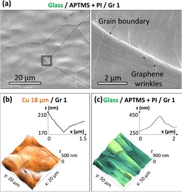
Figure 2. (a) SEM characterization shows clean and continuous Gr 1 transferred to APTMS + PI on glass by hot press. Graphene wrinkles together with imprinted Cu grain boundaries (originated in the Cu foil) can be observed. (b) AFM characterization of Gr 1 grown on Cu. The inset shows the section of the area marked in the map (grain boundary depth) by a squared dashed line. (c) AFM mapping of Gr 1 transferred to glass/APTMS + PI showing the imprinted Cu grain boundary. The inset shows the section of the area marked in the AFM map (squared-dashed line) which corresponds to the imprinted boundary that is lifted up as a consequence of the mechanical Cu peel-off.
Download figure:
Standard image High-resolution image3.2. Graphene transfer with laminator
For this case, the parameter 'Δx' was optimized to enhance the quality of transferred graphene using glass and PET as the final substrates. At Tc = 140 °C, and considering the substrate thickness, optimum values of Δx were 2 mm and 38 µm for glass and PET, respectively. It needs to be highlighted that this optimized Δx values are considered for the specific thickness of our substrates (1 mm and 125 µm for glass and PET, respectively). The use of substrates of different thickness would need to be optimized.
SEM and AFM characterization revealed differences compared to previous results. Figures 3(a) and (d) shows Gr 1 transferred to glass/APTMS + PI with more remarkable imprinted grain boundaries than the ones observed for the hot press transfer. According to the height profile in (d) of the area marked by the squared-dashed white line in the map, the imprinted grain boundary height using the laminator is almost three times higher than when transferring it with the hot press. Due to this, graphene grown on a less rough Cu foil—Gr 2- was tested to check if the imprint features to PI/graphene were reduced, thus improving the final quality of the material. In this case of Gr 2, the initial morphology of the Cu foil presented terraces instead of the large Cu grain boundaries of Gr 1, as demonstrated by AFM in figure S6. The differences in morphology of the transferred graphene are shown in figures 3(b), (c), (e) and (f), where Gr 2 was transferred to glass and PET, respectively. As before, the Cu terraces are imprinted to PI/graphene during the curing step, but showing less pronounced artefacts in this case. As it will be shown later with transmittance and electrical results, for lamination it can be concluded that the use of graphene grown on a low rough Cu foil is crucial for obtaining proper results. Finally, contact angle measurements were also measured confirming a high hydrophobicity of the PI/graphene surfaces with a mean value of 97° (figure S7).

Figure 3. SEM ((a)–(c)) and AFM characterization ((d)–(f)) of graphene samples transferred to glass/APTMS + PI ((a), (b), (d) and (e)) and PET/PI ((c) and (f)) using a laminator. Gr 1 was used for the transfer in ((a) and (d)) showing imprinted Cu grain boundaries with higher heights than for the hot press. Gr 2 was used for the transfer to glass ((b) and (e)) and PET ((c) and (f)) showing imprinted Cu terraces originated in the Cu foil (figure S6). Insets in the AFM characterization shows the section of the area marked in the mapping (squared-dashed line). Graphene was clean and continuous over the whole area of the samples and showed the morphology of the original Cu foil where it was grown.
Download figure:
Standard image High-resolution image3.3. Comparison of transfer processes
To assess the quality of the final structure, Raman analysis was performed to: (1) the original Cu foil where Gr 1 was grown, (2) spin coated VTEC on glass and cured at 150 °C without graphene on top, and (3) graphene samples transferred to glass/APTMS + PI and PET/PI by hot press and laminator techniques. Figure 4(a) shows the typical graphene spectra of a Cu/graphene foil, where the G and 2D peaks are detected at 1580 cm−1 and 2680 cm−1, respectively. The absence of a D peak and the I2D/IG ratio equal to 2 reveal the growth of high quality monolayer graphene. When transferring graphene to substrate/PI (figure 4(b)), the previous intense 2D peak appears very low as a consequence of the high absorption of PI—previously reported in literature [26]– which also hides the detection of the G peak. Due to this fact, Raman is used to verify the presence of graphene. The other peaks detected in the measurement at 1325 cm−1, 1376 cm−1, 1614 cm−1 and 1777 cm−1 are attributed to PI (light blue line), while the one at 1726 cm−1 is attributed to the PET substrate (top green line).

Figure 4. Raman characterization of (a) Gr 1 on Cu foil showing typical G and 2D bands of graphene and absence of D peak; (b) from bottom spectra to top: PI deposited on glass showing typical PI peaks (and absence of the 2D peak), and graphene transferred to glass and PET/PI by hot press and laminator showing peaks of graphene (very low 2D peak) and the corresponding substrate. The inset shows an amplification of the bottom measurement on glass/APTMS + PI to corroborate that the peak at 1325 cm−1 is also detected. This would confirm its attribution to PI and should not be confused with the graphene D peak. Peaks marked by (*) correspond to the PI layer.
Download figure:
Standard image High-resolution imageOptical measurements were carried out as the resulting product with transparency is important for applications, such as flexible displays or solar cells. Results were collected in figure S8 for samples transferred: (a) by hot press, (b) by the laminator to glass, and (c) by the laminator to PET substrates. All graphs include the transmittance of the bare substrate with and without PI (green and black lines, respectively). To determine the order of transparency of the samples, transmittances were calculated at 550 nm by removing the contribution of the substrate. Both data are collected in the bottom table 1. According to the results, samples with higher transmittance are:
Table 1. Transmittance (%) at 550 nm of graphene samples transferred by hot press and laminator techniques. Measured values (1st row) correspond to substrate/(APTMS+)PI/graphene. Calculated values (2nd row) correspond to the measured values where the substrate contribution has been removed (TCALCULATED = (TMEASURED × 100)/TSUBSTRATE). Below the table, transmittance reference values of substrates and PI/substrates are included
| T (%) at 550 nm | Hot press: Graphene to glass |
Laminator: Graphene to glass and PET |
||||||
|---|---|---|---|---|---|---|---|---|
| Gr 1, P(HP) = 250 | Gr 1, P(HP) = 200 | Gr 1, P(HP) = 300 | To glass | To PET | ||||
| Gr 2 Δx = 1 | Gr 1 Δx = 2 | Gr 1 Δx = 1 | Gr 2 Δx = 0.038 | Gr 2 Δx = 1 | ||||
| TMEASURED | 71 | 70 | 68 | 79 | 61 | 57 | 76 | 74 |
| TCALCULATED (no substrate) | 77 | 76 | 74 | 86 | 66 | 62 | 90 | 87 |
aTransmittance at 550 nm of: Glass = 92,36%; Glass/APTMS + PI = 89%; PET = 84.7%; PET/PI = 82%. bP(HP) units: psi. cΔx units: mm.
Gr 2/PET (laminator) > Gr 2/glass (laminator) > Gr 1/glass (hot press) > Gr 1/glass (laminator). If we compare the results obtained by lamination, graphene grown on the less rough Cu foil (Gr 2) is more transparent. As was shown before with SEM and AFM images (figures 3(a) and (d)), the imprinted grain boundaries to graphene/PI using Gr 1 (Cu foil of higher roughness) are more pronounced for the laminator than for the hot press. This increase of height at the grain boundary can scatter the light, thus leading to the observed reduction in transmittance. We believe that the transfer mechanism can be the main cause of this issue: while it is static for the hot press, the process is dynamic for the laminator with the sample being introduced 12 times. The continuous and progressive displacement of volatiles after each cycle might induce strain and defects in graphene at the imprinted Cu grain boundaries. We also speculate the combined effects of shear and compressive forces in the laminator could worsen the defect structures while only compressive force is in play in hot press.
Rs was measured by depositing Au/Ag paste electrodes on top of the graphene corners to measure carrier density (nS) and mobility (µH) following the procedure commented in supplementary information (figures S1(a) and (b)).
Figure 5 shows separately the obtained nS (red bubbles) for the hot press at different P(HP) values from 200 to 350 psi in (a), and for the laminator at Δx from 0.038 to 2 mm in (b,c). For a clear understanding of the results, we have indicated the graphene type used for each sample, Gr 1 being the only one used for the hot press transfer. In the case of the laminator, both graphene types were used, Gr 1 in samples S4 and S5 in (b), and Gr 2 in samples S6 and S7 in (c). The corresponding calculated values of µH (blue bubbles) calculated using the Drude model are plotted in (d), again making a distinction between the equipment and type of graphene used.
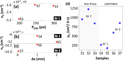
Figure 5. Hall measurements of the transferred graphene samples (S1–S7). The obtained nS is plotted for the different transfer methods. (a) nS obtained for samples S1–S3, fabricated with Gr 1 and transferred by hot press to glass/APTMS + PI at P(HP) of 200, 250 and 300 psi. (b) nS obtained for samples S4–S5, fabricated with Gr 1 and transferred by laminator to glass/APTMS + PI at Δx of 1 and 2 mm. (c) nS obtained for samples S6–S7, fabricated with Gr 2 and transferred by laminator to glass/APTMS + PI and PET/PI at Δx of 1 and 0.038 mm, respectively. (d) µH calculated for previous samples, specifying the type of transfer mechanism and type of graphene.
Download figure:
Standard image High-resolution imageThe seven samples (S1–S7) are obtained under different conditions. S1–S3 are Gr 1 samples transferred to glass/APTMS + PI using the hot press at different P(HP), while S4 and S5 are again fabricated with Gr 1 and transferred to glass/APTMS + PI, but using the laminator. S6 is fabricated with Gr 2 and transferred to glass/APTMS + PI, and S7 is fabricated with Gr 2 and transferred to PET/PI at the minimum Δx (0.038 mm).
In all cases (S1–S7), the graphene presents electron doping, with a stronger n-doping for the samples transferred with the laminator (S4–S7) as shown in figures 5(b) and (c). The reason for the n-type doping is that the graphene is transferred on PI, a material that could be positively charged due to unreacted amine groups from the aminosilane. This is contrary to the direct transfer of graphene to glass, a substrate that tends to be negatively charged due to deprotonated SiOH groups on the surface, thus leading to p-type doping into graphene.
For the samples obtained by the hot press in figure 5(a) at P(HP) from 250 to 350 psi, the mean value of Rs is equal to 1.9 kΩ sq−1. According to the results, the pressure does not seem to strongly affect the graphene doping, whose mean value is ( = −1.6 · 1012 cm−2). Nevertheless, the maximum value of µH equal to 1250 cm2 V−1 s−1 confirms the fact that the hot press allows the transference of high-quality graphene without low influence of the imprinted features on the PI/graphene.
For the samples obtained by the laminator in figures 5(b) and (c), it can be observed that the use of different substrates (glass and PET) do not have an effect on the graphene n-doping, whose mean value is ( = −1.4 · 1013 cm−2), as both target substrates are covered with PI. However, as previously mentioned, the laminator technique can induce defects onto the PI/graphene film due to the application of compressive and shear forces during the curing process, especially to the graphene grown on rougher Cu foils—Gr 1, (b)—which is confirmed by the SEM and AFM results in figures 3(a) and (d) above. These defects also contribute to the Rs, whose mean value is 3.5 kΩ sq−1, which is high if we consider the high doping measured. However, when the graphene grown on the less rough Cu foil—Gr 2, (c)—there is a great improvement in the transfer quality, as shown by the SEM and AFM results in figures 3(b), (c), (e) and (f) above. This is also confirmed by the Rs measurement, which has decreased to 770 Ω sq−1. This result is consistent due to the high level of carriers, as high doping reduces the Rs. The µH calculated for Gr 2 varies from 600 to 850 cm2 V−1 s−1, as can be observed on the right side of figure 5(d). Having selected a suitable Cu foil, we believe that the low µH observed is caused by the high carrier density. Further work needs to be devoted to understand the origins of the strong n-doping achieved by lamination, which might be related to the trapping of charges during the process. A proper control and reduction of doping in this technique would lead to an increase of µH.
After that, we wanted to demonstrate the stability of the samples to high temperature, to bending and to aqueous media in terms of Rs at different conditions.
The temperature stability of an already transferred sample—by hot press—was tested after depositing Au/Ag paste contacts on top of the graphene corners to measure Rs after each cycle of temperature. Three cycles of temperature were performed -from RT to 350 °C- where the sample was totally cooled down until RT before starting the next cycle. Figure S5 shows the graphene Rs measured between contacts where a current was injected through the two opposite contacts of the sample (see sample device in figure S1(b)). In all graphs, for the first cycle (empty red circle), it can be observed an increase of resistance from 150 °C to a range between 250 °C–275 °C after which the Rs decreased when temperature was raised until 350 °C. This increase is likely due to the shrinking of the PI. As shown initially in figure S2(b), at 150 °C the PI film contains approximately 4% of compounds that will evaporate at higher temperatures, with 4% being the difference between the weight loss of the PI film at 150 °C (83%) and the maximum weight loss of 87% at temperatures above 250 °C. This fact would explain the increase in the Rs, as the PI shrinks during the evaporation of volatiles, thus affecting the graphene that has been transferred onto it. Beyond 255 °C, which is the glass transition temperature (Tg) of PI [32], the PI film likely flattens due to increased relaxation dynamics. We hypothesize that this effect also flattens the graphene, thereby reducing the resistance.
For the next two cycles (after the samples were cooled down to RT), the initial Rs values were very similar to each other, but higher than for cycle 1 by approximately 1.3 kΩ sq−1. During the heating process for cycles 2 and 3 (half and full red circle, respectively), the Rs variation with temperature was linear, which is typical for conductive materials. Since the PI lost all volatiles at the end of the first cycle, no such sharp increase in Rs was observed in cycles 2 or 3. Thus, the mechanical and thermal stability of a glass/APTMS + PI/graphene composite at high temperatures after a first cycle of annealing could be confirmed.
The bending stability was evaluated on PET/PI/graphene samples at different radii of curvature (RB) to evaluate possible damage of graphene after several cycles. Figure 6(a) shows the Rs evolution of samples bent approximately at RB = 2 cm, 9 mm and 7 mm. Initially, Rs increases at RB1 = 2 cm (from 1130 to 1580 Ω sq.−1), but remains constant after 25 cycles. After 100 cycles at the lowest RB (RB3 = 7.3 mm), Rs increases again with a factor of 1.5. This indicates that the PI/graphene film might be damaged after the whole process.

Figure 6. Stability of transferred samples measuring Rs: (a) after bending tests of PET/PI/graphene at different RB. Rs increases by a factor of 2 after 130 cycles. Top pictures show the set-up where samples were bent at different RB (each area of the graph was bent at a different RB); (b) before and after dipping the samples S1, S6 and S7 in water for 5 min, demonstrating that graphene is not delaminated from the substrate/PI. For S6, Rs is practically constant after water immersion.
Download figure:
Standard image High-resolution image
The adhesion tests were performed to check graphene conductivity after dipping it in H2O for a period of 5 min (figure 6(b) and video 1 in supplementary material). For the situation where graphene is transferred directly to glass, after water immersion and due to the hydrophilic behavior of glass, the graphene would start to wrinkle and detach from the glass surface as the water would penetrate between them. In our case, we demonstrate that the graphene on glass or PET remains stable in an aqueous environment without delaminating. Although more statistics would be necessary to determine a possible increase of Rs after water immersion, we are certain about the fact that graphene physically does not delaminate from the substrate. The reason is the hydrophobic nature of PI, which is confirmed by the contact angle results of 95° in figure S7 and video 2 (supplementary material). Moreover, the addition of APTMS (0.5% wt. to PI) that could lead to slight positive charge in the substrate due to possible unreacted amine groups—and consequently to a hydrophilic surface- is also confirmed to be strongly hydrophobic, as it has been determined by the contact angles in figure S7 (supplementary information), where the water contact angle on cured PI + APTMS film are greater than 100° ((b) and (d) in figure S7). Because of that, we believe that our technique has a great potential for real product implementation since device fabrication often involves wet processes.
4. Conclusions
We have demonstrated a new technique to transfer graphene to glass and flexible substrates such as PET, using a mixture of PI and APTMS as an intermediate layer. Our technique is the first step towards making a substrate ready for device fabrication. The use of an intermediate thin leads to a device which is transparent, thermally stable (350 °C) and free of polymer residue—such as PMMA for the wet transfer method- on the device side of the graphene. Also, it has considered important aspects for industrial implementation, such as lower process times to previous techniques by a reduction of curing times, the Cu recyclability, the use of current industrial technology—a hot press and a laminator—and the demonstration of a high interfacial stability in aqueous media. While for hot press, the initial Cu foil does not represent an important consideration, for the lamination case we have found crucial the use of low rough Cu foils due to the foil artifacts are imprinted to graphene/PI structure. Although this work is based on a specific PI, it has been demonstrated that our technique is compatible to other materials, such as PAA, thus avoiding the limitation of our technique to a unique material. Further work will imply the understanding of graphene doping by the lamination technique and improvement of electrical mobility of graphene.
Acknowledgments
We acknowledge financial support from the Spanish Ministry of Economy and Competitiveness through the 'Severo Ochoa' Programme for Centres of Excellence in R&D (SEV-2015-0522) and OPTO-SCREEN (TEC2016-75080-R), from Fundació Privada Cellex, and from Generalitat de Catalunya trough the CERCA program. Partial support was also provided by Corning. Finally, we also acknowledge Dr James R Matthews for his help reviewing the manuscript.