
Abstract
The excellent electronic and mechanical properties of graphene allow it to sustain very large currents, enabling its incandescence through Joule heating in suspended devices. Although interesting scientifically and promising technologically, this process is unattainable in ambient environment, because graphene quickly oxidises at high temperatures. Here, we take the performance of graphene-based incandescent devices to the next level by encapsulating graphene with hexagonal boron nitride (hBN). Remarkably, we found that the hBN encapsulation provides an excellent protection for hot graphene filaments even at temperatures well above 2000 K. Unrivalled oxidation resistance of hBN combined with atomically clean graphene/hBN interface allows for a stable light emission from our devices in atmosphere for many hours of continuous operation. Furthermore, when confined in a simple photonic cavity, the thermal emission spectrum is modified by a cavity mode, shifting the emission to the visible range spectrum. We believe our results demonstrate that hBN/graphene heterostructures can be used to conveniently explore the technologically important high-temperature regime and to pave the way for future optoelectronic applications of graphene-based systems.
Export citation and abstract BibTeX RIS

Original content from this work may be used under the terms of the Creative Commons Attribution 3.0 licence. Any further distribution of this work must maintain attribution to the author(s) and the title of the work, journal citation and DOI.
1. Introduction
The concept of van der Waals heterostructures has led to a new technology of layer-by-layer engineering of two-dimensional (2D) materials with atomic precision [1, 2]. Out of the abundance of 2D materials, the two—graphene and hexagonal boron nitride (hBN), still remain the most unique couple, because of their outstanding synergetic properties. The hBN plays a vital role in ultra-high quality graphene devices [3, 4], and as an enabling material for graphene superlattices [5]. Besides, it is also known to protect sensitive 2D materials from environment via encapsulation [6]. Graphene, among its many superlatives, has the highest breakdown current density jmax ~ 1012 A cm−2 (assuming graphene thickness 3.4 Å), as measured in transmission experiments of accelerated (180 keV) xenon ions [7]. In electronic transport devices, the breakdown current densities of graphene are more modest, reaching ~5 · 108 A cm−2 in a vacuum (and much lower values in air) [8].
The high current-carrying capacity of graphene has made it a simple source of thermal infrared emission [9, 10]. Controlled by a bias voltage, a maximal emission temperature is limited to ~700 K due to heat dissipation to the metallic contacts and to the substrate [8, 10]. The latter mechanism dominates for graphene devices longer than a few microns. In the case of hBN encapsulated graphene devices, heat can also be efficiently dissipated through radiative heat transfer to hBN via its hyperbolic phonon polaritons [11]. Heat transfer is substantially reduced for suspended graphene devices, which leads to much higher emission temperatures approaching 3000 K, and to the emission in the visible spectrum (incandescence) when biased by electrical pulses under high vacuum [12]. But the stability of these devices in air is severely limited due to the oxidation of graphene [8, 12].
Metallic single-walled carbon nanotubes were also used as thermal light emitters, although, small saturation currents (<20 µA for a 3–4 nm diameter nanotube) and rapid oxidation in the air limit their use [13]. Interestingly, the electronic transitions between van Hove singularities led to a strong modification of the emitted spectra [13], which can be tuned even further by employing 1D photonic crystal cavities [14]. In this work, the encapsulation of graphene (Gr) with hBN allowed us to demonstrate robust incandescence of graphene devices in ambient conditions under continuous DC bias over extended periods of time. The hBN encapsulation provides excellent protection for graphene even at temperatures well above 2000 K, which we attribute to an unparalleled oxidation resistance of hBN [15–18]. Our study also reveals that dielectric cavity can support surface-guided waves at visible wavelength and tune the spectra of Planckian radiation.
2. Light emission from hBN-encapsulated graphene
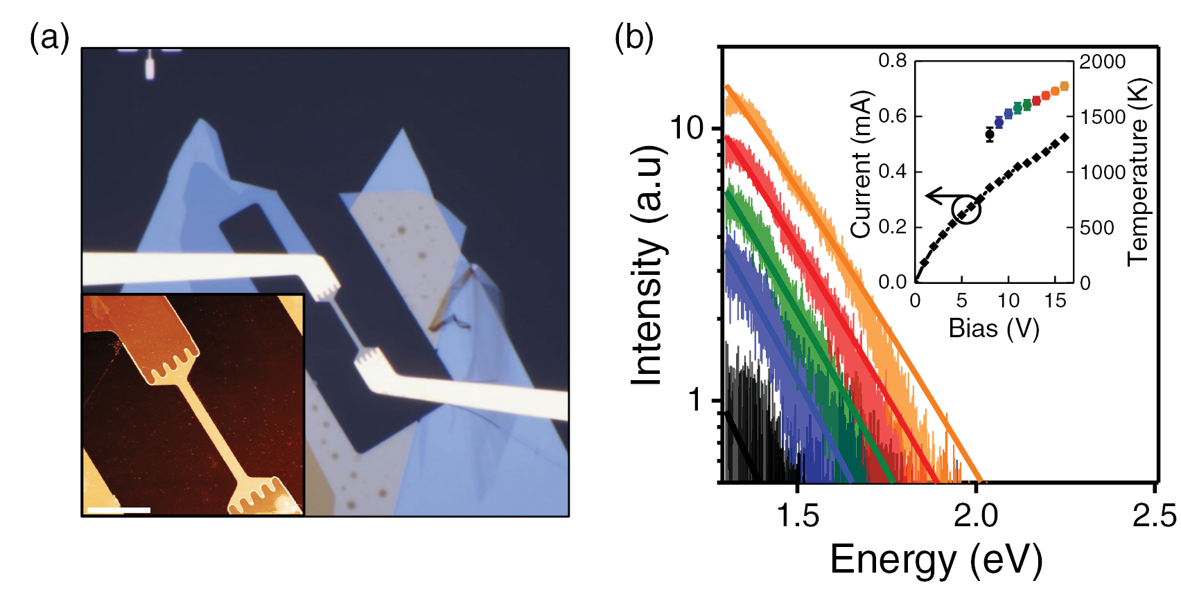
Figure 1(a) shows one of our hBN/Gr/hBN heterostructures fabricated on quartz substrate, using conventional dry peel technology followed by a standard e-beam lithography, dry etching and metallisation, as described elsewhere [4, 19]. We designed our devices such that the distance between the contacts is long enough (L ~ 10 µm) to avoid any effects from the contacts while keeping the contact resistance low by increasing the metal-to-graphene contact length. To characterise the light emission we pass a large current I (current density, j = I/W, reaching 600 A m−1) through a narrow (W ~ 1 µm is the channel width) graphene channel by applying a bias voltage Vb (estimated electric field E = Vb/L ~ 1.5 V µm−1, where L is the channel length). The supplied electric energy is transformed into Joule heat and dissipated in graphene, encapsulating hBN, quartz substrate, and metallic contacts, leaving a small fraction to radiate into free space. Figure 1(b) shows the emission spectra recorded using Renishaw Raman spectrometer equipped with Si-based CCD detector (diffraction grating 1200/mm; edge filter and beam splitter were removed during measurements). The obtained spectra are mostly featureless and can be described using Planck's law, modified by energy independent emissivity  (grey-body radiation) [9]:
where  is the photon energy, T is the temperature, c is the speed of light, kB and h are Boltzmann's and Planck's constants.

Figure 1. Thermal radiation of Joule-heated hBN/Gr/hBN device on quartz substrate, measured in ambient conditions. (a) Optical micrograph of hBN-encapsulated graphene filament. Inset: AFM image of the same device. Scale bar is 5 µm. (b) Thermal emission spectra from the quartz-supported device at different bias voltages (from 8 V to 16 V with 2 V step, grey to orange). Smooth lines are the fits obtained using equation (1). The inset shows current–voltage characteristics of the device, as well as the electronic temperatures extracted from the fits on the main panel.
Download figure:
Standard image High-resolution imageUsing equation (1) we obtained reasonable fits to the recorded emission spectra; extracted electronic temperatures and corresponding current–voltage characteristics are presented in the inset of figure 1(b). We also evaluated the model for light emission from graphene proposed in [12] but found that the spectra are indistinguishable from grey-body emission in the investigated spectral range. The emission efficiency (Pemission/Pelectric) of our devices was ~1.6 · 10−5, obtained using Stefan–Boltzmann law ( , A—device area, σ—Stefan–Boltzmann constant) and electrical power (
 ) similar to [9, 12]. For the emissivity (
 ) we used 0.023, following literature [9], the details can be found in the supplementary information (stacks.iop.org/TDM/5/011006/mmedia) (section 3).
Our devices demonstrated surprising long-term stability (many hours) at these very high current densities (>1.7 · 108 A cm−2), comparable with multilayer graphene-based infrared emitters but operated at much lower (7.1 · 106 A cm−2) current densities [10]. We further discuss a long-term stability and the mechanisms of breakdown in the supplementary information (section 1).
3. Enhancement of incandescence using photonic cavity
We prepared another set of hBN/Gr/hBN heterostructures but this time on SiO2/n-Si substrate and carried out the same high current light emission measurements, figure 2(a). We found that the emission spectra shift to the visible range and the graphene device incandesces (figures 2(b) and (c)). Considering this device is almost identical to that in figure 1, except for the presence of heavily doped silicon substrate, the drastic change in the emission spectra (see figures 1(b) and 2(c)) can be attributed to a resonance effect of a photonic cavity confined by the two interfaces: hBN/air and SiO2/Si, figure 2(d).

Figure 2. Incandescence in ambient conditions of Joule-heated hBN/Gr/hBN/SiO2/Si device. (a) Optical micrograph of hBN/Gr/hBN filament under illumination. (b) Its incandescence image captured by a monochrome camera. Scale bars in (a) and (b) are 5 µm. (c) Incandescence spectra (as well as theory curves, equation (2)) of the graphene device at different bias voltages (from 9 V to 23 V in 2 V steps, violet to dark red). The inset shows current–voltage characteristics of the device, as well as the electronic temperatures estimated from photonic cavity model, equation (2). (d) Schematic diagram of a Fabry–Pérot cavity of the air/hBN/Gr/hBN/SiO2/Si system.
Download figure:
Standard image High-resolution imageIt is instructive to analyse the parameters of this cavity using a simple model of a Fabry–Pérot resonator [20, 21]. The optical path length of the cavity  is ~740 nm for 290 nm SiO2 and 150 nm hBN/Gr/hBN stack. The refractive indices ni of SiO2 and hBN show negligible dispersion throughout the visible and near infrared spectral range, averaging at nSiO
 ~ 1.49 and nhBN ~ 2.05 [20, 22]. The reflectivities R of the 'mirrors' formed by hBN/air and SiO2/Si interfaces, are 0.12 and 0.19, estimated from Fresnel equations
  , where ni and nj are the refractive indices of the materials forming interfaces (with nSi ~ 3.8 and nair = 1, from [20]). These relatively low reflectivities lead to the output coupling losses, typically parametrised by the mirror coupling coefficients,
  in our case (2.1 and 1.7, for hBN/air and SiO2/Si mirrors, respectively). The expected photon decay time
  ~ 1.3 fs (
 the round trip time for the photon in the cavity) matches well the linewidth (ΔEmeasured ~ 0.5 eV, see
  ) of the measured emission peaks of figure 2(c) (extracted from experimental curves the linewidth values are presented in the figure S7 of the supplementary information). Furthermore, the observed peak maxima (~1.6 eV) are very close to the expected second mode of the cavity,
  eV.
eV.
We modelled the incandescence spectra by considering the grey-body radiation (equation (1)) modulated by a spectral line shape of the second mode of the cavity (using a Lorentzian,  , following [21]):

Surprisingly, this simplistic approach provides reasonable quality fits for the data (dashed lines in figure 2(c)), using temperature as the only fitting parameter. The extracted temperatures are presented in the inset of figure 2(c), the values are higher than for the device on quartz (see inset of figure 1(b)) because of the larger electrical power applied in the former case. Our temperatures were somewhat lower (1500–2500 K) in comparison with the emission (2500–2900 K) reported for suspended graphene [12]. We attribute this behaviour to the dissipation of heat to the surrounding media through hBN [11]. The hyperbolic phonon polaritons of hBN [23, 24] are predicted to efficiently (on a picosecond scale) cool hot graphene [11]. To reveal the interplay between the underlying physical mechanisms of cooling one need to perform time-dependent spatially-resolved thermal conductivity measurements, preferably on suspended hBN/Gr/hBN heterostructures, which is beyond the scope of this article.
Another effect of the photonic cavity can be seen in figure 2(b)—two rows of bright dots on the opposite ends of the device (their positions coincide with the tips of the gold comb electrodes). The gold electrodes are in thermal equilibrium with environment due to their macroscopic size and very good thermal conductivity, hence the temperature would be too low for the incandescence of the gold tips. On the other hand, the incandescent light from the central area of the device could travel through the waveguide formed by a photonic cavity all the way to the contacts, where it radiates possibly via coupling to gold plasmon modes at the contact edges [25]. The waveguide modes guide the graphene light emission over a long distance (at least 5–10 µm) even in this simple cavity, while the performance can be further improved by optimising the dielectric material and thickness to enhance the light emission [26, 27]. The frequency range of the photonic cavity modes can also be adjusted by optimising appropriate geometrical and material parameters.
4. Transport measurements in high-bias regime
To better understand the physics of graphene incandescence and to independently estimate the electronic temperatures in a high-bias high-current regime we performed four-terminal transport measurements on an hBN/Gr/hBN Hall bar device, figure 3. Electric field and current density values were obtained from measured 4-probe voltage Vxx, applied current I, and the geometry of the Hall bar (L × W is 2 × 1 µm2). At low biases, the current density increases linearly with the electric field and then deviates from the ohmic regime at |E| > 0.1 V µm−1, figure 3(a). This saturation tendency is typically attributed to the presence of in-plane acoustic and optical phonons [28–30], and other effects, such as Auger scattering [31].

Figure 3. Transport characteristics of a multi-terminal hBN/Gr/hBN Hall bar device, measured in a cryostat at 4 K. (a) Current density j versus electric field E at zero gate voltage. Top inset—device micrograph, scale bar 5 µm. Bottom inset—low-bias resistivity versus gate voltage. (b) Charge carrier density versus electric field (at zero gate voltage) measured from Hall effect (black circles), and estimated from self-gating field effect (dashed red line). The divergence at −1 V µm−1 is due to the change in the carrier type (the blue shaded region). (c) Electronic temperature extracted from data on the panel (b) using equation (3). (d) High electric field and high current induced non-equilibrium Fermi distribution limited by electron–phonon scattering processes. The energy values for in-plane graphene phonons (Γ-point optical phonons—blue line, K-point optical phonons—green line, and K-point transversal acoustic phonons—red line) are from phonopy [32].
Download figure:
Standard image High-resolution imageTo estimate the charge carrier density n, we measured our Hall bar device in a perpendicular magnetic field B, following the procedure described in [33]. The transversal voltage Vxy was linear with B within the measurement range of ± 2 T, allowing to estimate  at different electric fields, figure 3(b). At a non-zero temperature (T) and in the presence of disorder (Δn < 1010 cm−2) the measured carrier density is
where  is the thermally-induced carrier density, and vF is the Fermi velocity of electrons in graphene [34, 35]. The gate induced carrier density
  (εε0 and d are the dielectric constant and the thickness of gate dielectric) was estimated from the corrected gate voltage ΔVg, where the self-gating effect (due to large bias voltage) was taken into account, red dashed line in figure 3(b). Using equation (3) we estimated the effective electron temperature of graphene as a function of electric field, figure 3(c). The obtained temperatures are in range with those estimated from the emission spectra (figures 1 and 2).
Knowing the current density j and the charge carrier density n we extracted the drift velocity  , and the mobility
  at different electric fields (and, hence, temperatures). The vd slowly saturates starting at E ~ 1.5 V µm−1 reaching
  m s−1, almost 40% of the Fermi velocity. The mobility, high initially (~100 000 cm2 V−1·s−1), drops to below 1000 cm2 V−1·s−1 at high electric fields. From a simple Drude model we approximated the scattering time τ and the mean free path lmfp of the charge carriers from their mobility,
  . For independent scattering processes, the scattering time τ is dominated by the shortest process, which at high bias fields is usually the emission of the optical phonons [28, 36]. If the potential difference over the characteristic length lmfp is sufficiently high (
 ) a phonon of energy
  can be emitted resulting in the dissipation (heat) of electric energy in graphene lattice, and surrounding hBN and SiO2. This process, in turn, limits the lmfp, and bounds the non-equilibrium Fermi distribution, as shown on the cartoon in figure 3(d) (depicted as the tilt of the Fermi level). Figure 3(d) compares the characteristic energy
  against the typical (at high density of states in the phonon dispersion spectra) energies of representative phonon branches of graphene [37, 38]. Interestingly, the obtained characteristic energy values ~60 meV are sufficiently lower than graphene's in-plane phonon excitation energies, figure 3(d). Perhaps low energy acoustic phonons, longitudinal guided modes or other higher order acoustic modes at the interface of hBN and graphene limit the characteristic energy [37]. For a rather thin hBN substrate the characteristic energy might also be bound by optical phonons of SiO2 substrate [28].
5. Raman spectroscopy and lattice temperature
To complement the light emission and transport study, we performed Raman spectroscopy on our hBN/Gr/hBN heterostructures. To this end, we employed the same Renishaw spectrometer using 633 nm excitation laser line with incident power of 2 mW. The recorded spectra of the characteristic Raman peaks (G and 2D for graphene, E2g for hBN) for different bias voltages are summarised in figure 4. The intensities of all three peaks monotonically decrease with temperature. There is also a downshift with increasing temperature for all three peaks: 5 cm−1, 6 cm−1, and 7.5 cm−1 for G and 2D peaks of graphene, and E2g peak of hBN at the highest applied bias, respectively. The downshift of the G peak is attributed to the decay of Γ-point optical phonon into acoustic phonons through a range of phonon–phonon scattering processes [39]. Similar anharmonic decay processes (complicated by competing electron–electron scattering) of K-point optical phonons are also responsible for the downshift of the 2D peak of graphene [40, 41]. However, both G and 2D peaks tend to blue-shift as a result of doping [42] and strain [43], thus making it difficult to extract the correct lattice temperature from the Raman peak shift. Furthermore, the linewidth of the 2D peak is also affected by strain, for example, the nanometre-scale strain variations contribute to broadening of the 2D peak [44]. We, therefore, focus below on a linewidth of G peak as the most robust method.

Figure 4. Raman spectra of hBN/Gr/hBN device (same as in figure 2) at different bias voltages. (a) Raman spectra of G peak. (b) The linewidth of G peak as a function of temperature from phonon–phonon lifetime broadening (blue line), electron–hole plasma Landau damping (red line), and their sum (black line). The coloured circles (0–17 V, black to orange) are the experimental points extracted from the panel (a), plotted versus electronic temperatures extrapolated from emission spectra in figure 2. (c) Raman spectra of 2D peak. (d) Raman spectra of E2g hBN peak.
Download figure:
Standard image High-resolution image
We observed a non-monotonic behaviour of the linewidth γ(T) of the Γ-point phonon mode (G peak) with temperature, figures 4(a) and (b). This behaviour is in agreement with previous experimental observations, where linewidth of G peak is also first decreased and then increased with temperature [45]. We follow a simple model, considering two processes by which a Γ-phonon acquires a finite linewidth γG(T): by the anharmonic decay into two secondary acoustic phonons, γph–ph(T), or by creating an electron–hole pair (Landau damping), γe–ph(T,µ) [39, 45]. Here we ignore any higher-order anharmonic coupling processes. The total estimated linewidth of G peak  is plotted in figure 4(b) (black line; the anharmonic contribution and the Landau damping are the blue and red lines, respectively). We use 10 cm−1 and 3 cm−1 for γe–ph(0,0) and γph–ph(0), and include thermally-induced suppression of Landau damping, following procedures from [45, 46]. The γG values from figure 4(a) plotted as coloured circles versus electronic temperatures extracted from figure 2(c), are in a good agreement with the simple model suggesting the dominant anharmonic scattering mechanism.
Lastly, the hBN E2g peak is also downshifting and broadening with temperature (figure 4(d)) due to similar anharmonic phonon decay processes in hBN [47]. This suggests there is a strong heat transfer from graphene to the encapsulating hBN. Despite the heat dissipation in the encapsulating hBN layers, the electronic temperatures of graphene were well above 2000 K, as estimated from the incandescence spectra. Understanding the detailed mechanism of heat dissipation through the encapsulating hBN requires further theoretical investigations.
6. Conclusions
We demonstrated an interesting region of a parameter space (high current and electric field, high electronic and lattice temperatures), accessible in simple graphene/hBN heterostructures (and in the majority of existing devices) in ambient conditions. Electrically tunable light emission of graphene is modified by a photonic cavity formed at the interfaces, which can be further improved by optimising the parameters of the cavity. This atomically-thin light source is integrated with the cavity, which forms a waveguide, paving the way for new types of electrically-coupled photonic integrated circuits. This level of integration can be brought even further, by combining the photonic circuit elements with electrically-driven phononic and mechanical modes. We believe our study will stimulate further experimental and theoretical work in this fascinating research direction, where many interesting questions are now open, such as the understanding the mechanisms of heat dissipation in these devices, including the effects of hyperbolic phonon polaritons in hBN.
Acknowledgments
This work was supported by EU Graphene Flagship Program, European Research Council Synergy Grant Hetero2D, the Royal Society, Engineering and Physical Research Council (EPSRC), and US Army Research Office (W911NF-16-1-0279). Servet Ozdemir acknowledges PhD studentship from EPSRC funded Graphene NOWNANO CDT. Artem Mishchenko acknowledges the support of EPSRC Early Career Fellowship EP/N007131/1.