

Abstract
Schottky barriers greatly influence the performance of optoelectronic devices. Schottky barriers can be reduced by harnessing the polymorphism of 2D metal transition dichalcogenides, since both semiconducting and metallic phases exist. However, high energy, high temperature or chemicals are normally required for phase transformation, or the processes are complex. In this work, stable low-resistance contacts between few layer MoTe2 flakes and gold electrodes are achieved by a simple thermal annealing treatment at low temperature (200–400 °C). The resulting Schottky barrier height of the annealed MoTe2/Au interface is low (~23 meV). A new Raman Ag mode of the 1T' metallic phase of MoTe2 on gold electrode is observed, indicating that the low-resistance contact is due to the phase transition of 2H-MoTe2. The gold substrate plays an important role in the transformation, and a higher gold surface roughness increases the transformation rate. With this method, the mobility and ON-state current of the MoTe2 transistor increase by ~3–4 orders of magnitude, the photocurrent of vertically stacked graphene/MoTe2/Au device increases ~300%, and the response time decreases by ~20%.
Export citation and abstract BibTeX RIS
Introduction
Two-dimensional (2D) atomic crystals have potential applications in electronics [1–5], photonics [6–11] and energy conversion [12–14]. Compared with graphene, transition metal dichalcogenides (TMDs) are more attractive for future optoelectronics applications because of their intrinsic band gaps (1–2 eV) and high photosensitivity [15]. The realization of low-resistance contacts between the channel and metallic electrodes is a key issue for optimizing the performance of TMD-based devices since Schottky barriers at the interface limit carrier injection, resulting in the reduction of carrier mobility, current, and so on.
Detailed studies have demonstrated that metallic electrodes with the Fermi level close to the edge of the conduction band (CB) for n-type or valence band (VB) for p-type semiconducting TMDs, respectively, can mitigate the Schottky barrier and decrease contact resistance [16, 17]. Chemical doping can also modulate the Fermi level of TMDs close to that of metallic electrodes, thus reducing the contact resistance [18]. The contact resistance has been lowered by introducing other 2D materials into the TMD/metal interface, such as graphene [19] or hexagonal boron nitride [20], but the preparation process is more complex. Alternatively, inducing a metallic interlayer between semiconducting TMDs and metal electrodes by phase engineering provides a more direct approach to achieve ohmic contact. So far, it has been demonstrated that phase engineering can be realized by e-beam irradiation [21], laser irradiation [22], plasmonic hot electron injection [23] and organolithium treatment [24, 25], but these methods are complicated or contamination could be introduced in the treatment process.
Molybdenum ditelluride (MoTe2) can exhibit stable 2H and 1T' phases, corresponding to the semiconducting and metallic phases, respectively. The 2H phase can transform to 1T' phase at temperatures above 880 °C [26, 27], however, the temperature of the phase transition can be lowered to ~650 °C with the help of Te vacancies [27]. Theoretical calculations predict that few-layer MoTe2 can be transformed from semiconducting 2H phase to metallic 1T' phase by applying 0.2–3% strain even at room temperature [28]. Thus, it is an interesting challenge to optimize the phase transition of this 2D material. With a band gap of ~1.0 eV, 2H-MoTe2 is sensitive to near-infrared light and can be realized as broadband photodetectors, making it attractive for 2D optoelectronics.
Here we demonstrate a simple method to significantly reduce the Schottky barrier at the MoTe2/Au interface. After thermal annealing at 400 °C in nitrogen atmosphere, both the field effect mobilities and ON-state currents of the field effect transistors based on MoTe2 flakes increase by 3–4 orders of magitude. Raman mapping images show that a new Raman peak appears, suggesting that the improved performance is due to MoTe2 phase transition from the semiconducting phase to metallic phase at low temperatures (200–400 °C). The extracted Schottky barrier height of the treated MoTe2/Au interface reduces to ~23 meV. We find that the morphology of the Au film plays an important role in the phase transition process. The rougher the Au surface, the higher the phase transformation rate of the 2H-MoTe2 flakes. With this method, the phase transition is also realized in vertically stacked graphene-MoTe2-Au devices. The photocurrent of the vertical transport photodetector increases by ~300%, and the response time decreases by ~20%.
Experimental section
Materials
MoTe2 single crystals were purchased from Smart-Elements company. Ti and Au 99.99% were purchased from Kurt J. Lesker company.
Methods
Preparation of Au electrodes with different thickness
Polymethylmethacrylate (PMMA) layers were spin-coated on 300 nm SiO2 covered Si wafers. Contact electrodes were patterned via E-beam lithography techniques (EBL Jeol JBX-6300FS). The wafers were immersed in the solution of methyl isobutyl ketone (MIBK) and isopropanol (IPA) (1:1) for 30 s and then washed in IPA for 30 s. Au/Ti electrodes were deposited on them by using thermal evaporator (Kurt J. Lesker Nano 36). In the evaporation process, a layer of 3 nm Ti was deposited at first as a bonding layer, and then different thicknesses (15, 45, 85 nm) of gold were deposited to prepare gold electrodes with smooth, medium and rough surfaces. To remove PMMA, the wafers were immersed in acetone for 8 h, washed repeatedly by IPA and dried in N2 flow. Au/Ti electrodes were thus prepared on Si/SiO2 (300 nm) wafers.
Mechanical exfoliation and transfer of MoTe2 crystals
MoTe2 crystals were mechanically exfoliated onto a transparent elastomeric stamp (polydimethyl siloxane, PDMS) as previously reported [29]. Few-layered MoTe2 were selected via optical microscopy and Raman spectroscopy. For the fabrication of MoTe2 transistors, the exfoliated MoTe2 were transferred on top of prepared gold electrodes using a transfer station equipped with a microscope.
Preparation of graphene/MoTe2/Au photosensor
On the Si/SiO2 (300 nm) wafer, the MoTe2 flake was transferred onto Au bottom electrode as described above, and graphene top electrode was transferred by a wet transfer process as follows. Graphene (GR) is grown on copper foil as reported in previous work [30]. In a typical wet transfer process [31], PMMA layer was spin-coated on GR/Cu foil and then baked at 180 °C for 2 min. To etch the copper, the PMMA-coated Cu foil was placed in an ammonium persulfate solution (1.5 %wt) for 8 h, and then washed by ultrapure water three times. The floating PMMA/GR film was lifted out by the wafer substrate with MoTe2/Au, followed by drying at 60 °C for 1 h. After that, the sample was heated at 130 °C for 10 min ro achieve close contact. Graphene electrode was inversely patterned via E-beam lithography techniques, meaning the electrode is protected by PMMA and unexposed to E-beam. After developing in MIBK and washing in IPA, the sample was treated by oxygen plasma (20 W, 30 s) to remove the exposed graphene. Finally, the PMMA layer was removed by immersing in acetone for 12 h.
Annealing of MoTe2 transistors
The prepared MoTe2 devices were annealed in N2 atmosphere at 400 °C for 30 min with 10 °C min−1 heating rate, and then cooled down naturally to room temperature. For the control device, MoTe2 flakes were transferred on gold electrodes preheated at 450 °C for 2 h. Similar control experiments have been previously reported [32].
Characterization
Atomic force microscopy (AFM) was performed on a BRUKER Dimension FastScan in ambient environment, and the image scanning rate was 3 Hz and resolution 256 × 256. Markers were made to locate the same place on gold electrode. Electrical characterization was performed in a Agilent B2912A system in ambient environment. Raman measurements was performed using a WITEC-Alpha 300 R with a 100× objective. The laser wavelength used was 532 nm, laser power was 24 µW, and accumulated time was 10 s. Photocurrent mapping was performed by combining Raman spectroscopy with electrical measurements.
Results and discussion
Field effect transistors (FETs) based on few-layer MoTe2 are fabricated by mechanically exfoliating MoTe2 flakes on polydimethyl siloxane (PDMS) stamp, and then dry transferring onto gold film electrodes, which are prepared by a standard photo lithography process. Atomic force microscope line scans (figure 1(a)) show that the thickness of the exfoliated MoTe2 flake is ~5.8 nm, corresponding to 8 layers [33]. After thermal annealing treatment at 200, 300 and 400 °C in nitrogen atmosphere, the electrical transport properties of the few-layer MoTe2 FET are measured at room temperature in ambient air. As shown in figures 1(c) and S1, the Ids–Vds curves change from nonlinear to linear, suggesting that Schottky barrier height at the interfaces between the few-layer MoTe2 and gold electrodes decreases, and contact resistances consequently decrease. After annealing at 400 °C, the transfer curve of the device displays p-type behaviour (figure 1(d)), which is consistent with previous reports [34], and the drain current in ON state increases to 6 × 10⁻⁶ A at Vds = 1 V, Vg = −50 V, which is about 4 orders of magnitude higher than that of the pristine device (figure S1 (stacks.iop.org/TDM/4/045016/mmedia)). This indicates that the resistance of the device decreases dramatically, consistent with the linear behaviour of the Ids–Vds curve, and low-resistance contact is formed at the MoTe2/Au electrode interfaces. Using the equation µ = Lgm/(WCoxVds), where L, W, Cox, gm are the channel length, width, gate capacitance, and transconductance at a particular Vds, respectively, the electric field mobility of the device can be extracted. As shown in figure 1(e), the mobilities increase three orders of magnitude from 0.01 to 15 cm2 V−1 s−1 after increasing the annealing temperature from 200 to 400 °C, comparable to few-layer MoTe2 FETs (~50 cm2 V−1 s−1) modified by laser-induced phase patterning [22]. It is reasonable to presume that the high mobility of the device after annealing could be due to low-resistance contact formation at the MoTe2/Au electrode interface, leading to increased carrier injection efficiency. We fabricated 4 devices, and the mobilities after annealing at 400 °C ranged from 12 to 26 cm2 V−1 s−1, indicating that this method is a stable and reproducible method way to improve performance of MoTe2 transistors. Based on equation (1) and thermionic emission theory [35–37], the effective Schottky barrier height ΦB of MoTe2/Au interface at various gate bias (figure 1(g)) can be extracted from the slope of the lines in Arrhenius plot (figure 1(f)).
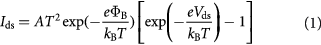
where Ids is the source–drain current, A is the Richardson constant, T is the absolute temperature, kB is the Boltzmann constant, e is the electron charge, ΦB is the effective Schottky barrier height, Vds is the source–drain bias. As discussed in detailed in previous articles, the true ΦB is extracted when the applied gate bias is equal to the flat band voltage (Vg = VFB) [35]. When Vg is higher than VFB, the effective barrier height is linear to the applied gate voltage, where the drain current is dominated by thermionic emission at the MoTe2/Au interface. When Vg is lower than VFB, the effective barrier height deviates from the linear trend, where the thermally assisted tunneling effect at the MoTe2/Au interface becomes to affect the source–drain current. Therefore, in the ΦB versus Vg plot (figure 1(g)), the bias value corresponding to the point deviates from the linear region is VFB, and the barrier height at this point is the true ΦB, which is 23 meV in this study. Moreover, the contact resistance at modified MoTe2/Au interface is estimated to be 6 kΩ µm when Vg = −50 V (figure S10), and it is much lower than the reported MoTe2/Au contact resistance (75 kΩ µm) [38]. Thus, Schottky barrier at MoTe2/Au interface is reduced, and low-resistance contact is achieved by a simple thermal annealing method.

Figure 1. (a) Atomic force microscopy image of a few-layer MoTe2 device fabricated on gold electrodes, the scale bar is 5 µm. (b) Scheme of few-layer MoTe2 FET. (c) Ids–Vds curves of the MoTe2 FET after 400 °C annealing, the gate bias sweeps from −50 to +50 V with 25 V step. (d) Transfer curves (Ids–Vg) of the MoTe2 FET after 200, 300, 400 °C annealing (Vds = 1 V, measured at room temperature in ambient air), inset is the corresponding semi-logarithmic graph. (e) Calculated hole mobilities of the MoTe2 FET after 200, 300, 400 °C annealing. (f) Arrhenius plot of phase-engineered MoTe2 FET for various gate biases, the data corresponding to biases above 0.25 V start to present poor linear tend, indicating VFB is around 0.25 V. (g) Extracted effective barrier height as a function of gate bias. (h) Output curves (Ids–Vds) of MoTe2 FET fabricated on the pre-annealed gold electrodes, electrodes were annealed at 450 °C for 2 h before fabrication and then the fabricated MoTe2 FET was annealed at 400 °C.
Download figure:
Standard image High-resolution imageAs the FET is fabricated by transferring MoTe2 flakes onto gold electrodes, the contacts are not so intimate, and the interactions between gold electrodes and MoTe2 flakes are weak with high Schottky barriers [39]. It is well known that thermal annealing is a good way to improve the quality of contact between metal and TMD materials, mainly because annealing can clean the TMD surface and subsequently induce intimate contact. In the control experiment, the Au electrodes are pre-annealed at 450 °C for 2 h, then transferring the MoTe2 flake onto the annealed gold electrodes, and finally annealed the device at 400 °C again. As shown in figure 1(h), this control FET exhibits poor output curves after 400 °C annealing, indicating the Schottky barrier height is not reduced in this case, which means the effect of annealing is limited. Furthermore, we prepare bottom-contact MoTe2 FET with thermal-evaporated gold electrodes on prepared MoTe2 flakes, which also displays Schottky contact behaviour after 200–400 °C annealing (it will be discussed below in figure 3). From the above results, we can conclude that surface cleaning and intimate contact does not dominate the improvement of MoTe2 FET performance in this study, and there must be other effects induced at the MoTe2/Au interface to achieve the ultralow-resistance contact for the top-contact MoTe2 FETs.
As Au atoms can bond to most chalcogens including Te [40, 41], thermal annealing may facilitate the formation of Au–Te bonds and charge transfer at the MoTe2/Au interface, resulting in improved contact. This hypothesis can be also ruled out by our control experiments, since the MoTe2 FETs with preheated or top gold electrodes do not present low-resistance contact after annealing. In previous studies, surface reshape is observed when evaporated metal (Pd, Au, Ag) film is annealed [42, 43], which means their surface atoms reconstruct after annealing. In this study, we propose that the gold surface reshaping process may induce strains in MoTe2. As previously demonstrated, the semiconducting 2H to metallic 1T' phase transition can be achieved by inducing strain, and especially for MoTe2, weak strain (~0.3%) is sufficient for phase transition [26]. Therefore, we postulate that the ohmic contact is caused by the phase transition of MoTe2.
Raman spectroscopy is an effective way to characterize the phase of MoTe2 [22], and Raman spectra and mapping scans were performed after a series of annealing treatments (figure 2). As shown in figure 2(a), the pristine MoTe2 flake exhibits sharp peaks corresponding to the  mode at ~235 cm−1 and A1g mode at ~174 cm−1, which are the characteristic signatures of the hexagonal (2H) phase of bulk MoTe2 [27]. The
  peak at 290 cm−1 is also observed, indicating the exfoliated 2H-MoTe2 crystal is few-layered [34, 44]. The peaks near 139 and 185 cm−1 are attributed to second-order Raman modes of 2H-MoTe2 [45]. After thermal annealing at 400 °C, the Raman spectrum of few-layer MoTe2 on SiO2/Si substrate hardly changes, indicating the few-layer MoTe2 in the channel of the device remains in the semiconducting 2H phase. In contrast, the Raman spectra of MoTe2 on the gold electrodes show a new peak at ~123 cm−1, which is reported to correspond to the characteristic Ag mode of metallic phase of MoTe2 [22]. Figure 2(c) are the Ag mode Raman intensity mapping images for the pristine MoTe2, acquired after annealing at 200, 300, and 400 °C, respectively. From these images, we can find that, with the increase of the annealing temperature for the few-layer MoTe2 on the gold electrode, there are more areas where the Ag peak is observed, and the Ag peak intensities increase with the annealing temperature. This suggests that semiconducting 2H-MoTe2 has been tranformed to the metallic phase in larger regions on the gold electrode, resulting in low-resistance contact at the MoTe2/Au interface.

Figure 2. (a) Raman spectra of a few layer MoTe2 flake on Au and SiO2/Si substrates before and after annealing, and the spectra from bottom to top are respectively few-layered MoTe2 on SiO2/Si, MoTe2 on Au, MoTe2 on SiO2/Si and Au after 400 °C annealing. (b) Optical microscopy (OM) image of the few-layered MoTe2 flake on SiO2/Si substrate and Au electrode surface, with a red rectangle indicating the Raman mapping scanning area. (c) Corresponding Raman mapping images (Peak position at 123 cm−1) from MoTe2 (pristine, 200, 300 and 400 °C annealed), the boundary of Au is marked by white dot line.
Download figure:
Standard image High-resolution imageIn previous studies, the metallic phase of MoTe2 is induced by strain or high power laser irradiation [22, 26]. To exclude the effect of laser-induced phase transition of few-layer MoTe2 in the Raman experiments, the laser power was set at ~24 µW, which proved to be unable to induce the phase transition (figure S3). As shown in the Raman peak position mapping image (figure S4), a red-shift of 1 cm−1 is observed on annealed MoTe2/Au, indicating tensile strains are induced in MoTe2, consistent with a previous Raman study on TMDs flakes, where a red-shift of 1 cm−1 for the E2g mode was observed when applying in-plane 1% strains [46, 47]. As mentioned above, phase transition of MoTe2 at room temperature just requires a strain of 0.3% [26, 28], which has been achieved in this study. Moreover, the highest mobility and highest ON-state drain current of the MoTe2 FET after annealing at 400 °C are consistent with the phase transition of the few-layer MoTe2 on the gold electrodes. Thus, we suggest that strain induces a phase transition from semiconducting to metallic phase for the few-layer MoTe2 on gold film, resulting in lower Schottky barrier and lower contact resistance at the MoTe2/Au interface.
Compared to the phase transition of the MoTe2 flake on Au electrodes, the Raman Ag mode of the metallic phase is not observed for the MoTe2 flake on SiO2/Si substrate (figure 2), which means that the phase transition does not occur for the MoTe2 flake on SiO2/Si substrate, suggesting that the Au substrate plays an important role in the phase transition process. To clarify the effect of the Au substrate, the morphology of an Au film (~85 nm thick) without the transferred MoTe2 flake is measured before and after thermal annealing at 400 °C. As shown in the AFM images of the same area before and after annealing (figure S5(a)), the morphology of the annealed Au film obviously changes, indicating that the thermal annealing can make the Au atoms move and the surface reconstruct. To quantify the change of partial surface roughness, root-mean-square roughness (Rq) values are measured in the two new hillock regions (figure S5(b)), and the corresponding Rq values increase respectively from 1.35 to 1.77 nm and from 1.35 to 2.05 nm after 400 °C annealing. After thermal annealing, we observed the gold surface reshaping in AFM images (figure S5), Raman peak shifts (figure S4), and new phase formation of MoTe2 (figure 2) in the Raman study. From these results, we propose that the annealing-induced reconstruction of Au surface can induce strains in the MoTe2 flakes, resulting in the new MoTe2 phase. In the case of MoTe2 FET with preheated gold electrodes, reannealing cannot induce gold surface reconstruction again on the preheated gold electrodes (figure S6), so no strain and metallic phase of MoTe2 can be induced, resulting in the poor contact (figure 1(h)).
We also studied the annealing effect on the bottom-contact MoTe2 transistor with top gold electrodes (figures 3(a)–(d)). Interestingly, the Ids–Vds curves did not become linear with the increase of annealing temperature, and the drain current at the same Vds and Vg is smaller than that of top-contact MoTe2 FETs, indicating that the Schottky barrier height is still high and thermal annealing cannot improve the contact in this case. To analyze the phase of the MoTe2 in this case, the annealed MoTe2/top-Au is prepared on a transparent quartz substrate so that Raman laser can irradiate the gold-covered MoTe2 flake from the bottom (as shown in figure 3(e)). From the Raman mapping images (figure 3(f)), there is no signature peak of metallic phase MoTe2, indicating top-layer gold surface reconstruction cannot induce phase transition of bottom-layer MoTe2. Therefore, without phase engineering, the Ids–Vds curves of the bottom-contact MoTe2 transistor exhibit nonlinear behavior, the ON state current are smaller than that of the top-contact MoTe2 FETs.

Figure 3. (a) Scheme of few-layer MoTe2 FET with top gold electrodes. (b)–(d) Output curves (Ids–Vds) of MoTe2 FETs with top gold contact electrodes after a series of annealing. (e) Scheme of Raman test of MoTe2 flake with top gold after 400 °C annealing. (f) Optical microscopy image of MoTe2 flake with top gold and corresponding Raman mapping, the scale bar is 10 µm.
Download figure:
Standard image High-resolution imageTo further confirm the morphology effect on phase transition, Au electrodes with different surface roughness was prepared by controlling the deposition conditions of the thermal evaporator [42, 48]. As shown in figures 4(a)–(c), three categories of surface roughness were prepared, and the measured Rq values are 2.08, 1.08 and 0.43 nm, respectively, corresponding to the rough, medium and smooth Au electrodes. Few-layer MoTe2 flakes were transferred onto these electrodes, and Raman mapping performed after annealing treatment at 400 °C (figures 4(d)–(f)). As shown in figures 4(d)–(f), the Raman intensity of the Ag mode is the strongest for the MoTe2 flakes on the rough Au electrode, while it is the weakest for the MoTe2 flakes on the smooth Au electrode, indicating the roughness of the Au electrode is directly correlated to the phase transition probability of the MoTe2 flakes. As it has been shown that the phase transition is induced by strains, we presumed that strains can be adjusted by annealing gold with different surface roughness and consequently induce varying degrees of MoTe2 phase transition. The electrical transport properties are measured for the three categories of devices (figures 4(g)–(i)). It is found that the Ids–Vds curves are the most nonlinear for the device with the smooth Au electrode, suggesting that the Schottky barrier at the contact interface is the highest when the phase transformation rate is too low. In contrast, the Ids–Vds curves become linear for the device with the rough Au electrode, and the low-resistance contact is achieved with metallic phase formation. In summary, the roughness of the Au electrode can influence the phase transition of the MoTe2 flakes, and the phase transformation rate of the 2H-MoTe2 flakes is directly correlated to the surface roughness of the Au electrodes.

Figure 4. (a)–(c) Atomic force microscopy 3D surface images of gold electrodes with different roughness. (d)–(f) Optical microscopy images (left) and corresponding Raman intensity mapping (right) images of Ag peak after 400 °C annealing MoTe2 FETs with different rough gold electrodes, the scale bar in OM and Raman images are 10 µm and 800 nm, respectively. (g)–(i) Ids–Vds curves of the annealed MoTe2 FETs with different rough gold electrodes, gate bias sweeping direction is marked as arrow direction, and the sweeping step is 12.5 V.
Download figure:
Standard image High-resolution imageLow-resistance contact can also be achieved in vertically stacked graphene/MoTe2/Au devices by our method. As shown in figure 5(a), a few-layer MoTe2 flake (red dot line) is transferred onto an as-prepared Au film (blue dot line), and then a CVD-grown monolayer graphene (black dot line) is transferred onto the MoTe2 flake. To ensure vertical charge transport, the top graphene layer is smaller than the MoTe2 flake, and located directly above the MoTe2 flake (figure 5(b)). In the vertical transport device, the Au film and top graphene layer are the bottom and top electrodes, respectively. From the Raman mapping images (figures 5(c) and (d)), the characteristic Raman Ag peak of metallic MoTe2 is observed, suggesting phase engineering can be achieved on MoTe2/Au even if other 2D materials (e.g. Graphene) are used as the top (transparent) electrode. Compared with other strategies such as laser or E-beam irradiation, our work shows great potential in the phase engineering of vertical MoTe2 devices. Laser and E-beam irradiation may cause unintended beam damage or modifications to the device structure [22]. For our graphene/MoTe2/Au vertical device, the photocurrent (Iph = Ilight − Idark) mapping images are taken at Vds = 0.1 V and illuminated by a continuous wave (CW) 532 nm laser at ~24 µW, and the photoresponsivity (R = Iph/Plight) is calculated to be 46 mA W−1. As shown in figure 5(e), the photocurrent is higher in the phase transition area, indicating photo-generated electron-hole pairs are more efficiently separated and collected by the electrodes [6, 49]. Compared with the photocurrent of the device before thermal annealing (figure 5(f)), after the phase transition of the MoTe2 flake, the photocurrent increases about ~300%. Figure 5(g) shows the time-resolved photoresponse of the device, and the rise and decay times are respectively defined by the increase in photocurrent from 20% to 80%, and the corresponding decrease from 80% to 20% of the maximum photocurrent [50]. Clearly, the rise time decreases from 131 to 96 ms, while the decay time decreases from 114 to 95 ms after annealing. Thus, an MoTe2/Au ohmic contact can also be achieved in a vertically stacked photosensor, resulting in higher photosensitivity and faster photoresponse.

Figure 5. (a) Optical microscopy image of vertically stacked Graphene/MoTe2/Au device, the edges of graphene, MoTe2 and Au correspond to the black, red and blue dotted lines, respectively. (b) Scheme of vertically stacked Graphene/MoTe2/Au device (c) and (d) Raman intensity mapping of 2H-MoTe2 ( : ~238 cm−1) and metallic phase of MoTe2 (Ag: ~123 cm−1) corresponding to the region defined by the black solid rectangle in figure (a). (e) Photocurrent mapping corresponding to the black solid rectangle in figure (a) illuminated with focused laser (532 nm, ~24 µW, bias voltage is 0.1 V). (f) Time-resolved photoresponse of the vertical photodetector before and after annealing (638 nm, 0.94 mW laser, bias voltage is 0.1 mV). (g) Photoswitching rate of the photodetector before and after annealing (638 nm, 0.94 mW laser, bias voltage is 0.1 m V).
Download figure:
Standard image High-resolution image
Conclusion
In summary, the Schottky barrier between Au and MoTe2 flakes is significantly reduced by simple thermal annealing at 400 °C in a nitrogen atmosphere. The characteristic Raman Ag peak of metallic phase MoTe2 is observed at the interface between MoTe2 flakes and Au electrodes, indicating that the reduction of Schottky barrier results from the phase transition observed in the 2H-MoTe2 flakes. We find that the transformation rate to the metallic phase is directly correlated to the roughness of the Au electrode substrate. In this work, we have demonstrated a simple phase engineering process for ohmic contacts at the MoTe2/Au interface, and as no chemicals are introduced, this method could have important applications in future optoelectronics based on 2D materials.
Supporting information
Supporting Information is available from the IOP Online Library or from the author.
Acknowledgments
This work was supported by the National Science Foundation of China (Grant No. 51472164), the 1000 Talents Program for Young Scientists of China, Shenzhen Peacock Plan (Grant No. KQTD2016053112042971), the Educational Commission of Guangdong Province project (Grant No. 2015KGJHZ006), the Science and Technology Project of Guangdong Province (Grant No. 2016B050501005), the Educational Commission of Guangdong Province (Grant No. 2016KCXTD006), the Natural Science Foundation of SZU (Grant No. 000050 and No. 2017029), and the China Postdoctoral Science Foundation (2015M582415). ATSW acknowledges financial support from ASTAR Pharos Project No. 144-000-359-305. We also acknowledge Junyong Wang (PhD student, National University of Singapore) for his help in electrical characterization.
Conflict of interest
The authors declare no competing of financial interest.