

Abstract
The emergence of two-dimensional (2D) materials has attracted a great deal of attention due to their fascinating physical properties and potential applications for future nano-electronic devices. Since the first isolation of graphene, a Dirac material, a large family of new functional 2D materials have been discovered and characterized, including insulating 2D boron nitride, semiconducting 2D transition metal dichalcogenides and black phosphorus, and superconducting 2D bismuth strontium calcium copper oxide, molybdenum disulphide and niobium selenide, etc. Here, we report the identification of ferromagnetic thin flakes of Cr2Ge2Te6 (CGT) with thickness down to a few nanometers, which provides a very important piece to the van der Waals structures consisting of various 2D materials. We further demonstrate the giant modulation of the channel resistance of 2D CGT devices via electric field effect. Our results illustrate the gate voltage tunability of 2D CGT and the potential of CGT, a ferromagnetic 2D material, as a new functional quantum material for applications in future nanoelectronics and spintronics.
Export citation and abstract BibTeX RIS
Introduction
The research on graphene and post-graphene two-dimensional (2D) materials has been one of the most exciting research fields in the last decade [1–17]. Graphene is a Dirac material that has exhibited a lot of interesting/superior physical properties, including extremely high mobility, room temperature quantum Hall effect, and long spin lifetimes [1–4, 13, 17]. 2D boron nitride is an insulating material, which can be used as a tunneling barrier or a protecting layer for other 2D materials [7, 8, 10]. Semiconducting 2D transition metal dichalcogenides and black phosphorus could be very useful for nano electronics devices [6, 7, 9, 14, 16], such as field effect transistor with large on/off ratio. Superconducting 2D materials also provide interesting physical properties, such as Ising superconductivity [11, 12, 18]. Furthermore, the structures consisting of various 2D materials, van der Waals structures, have shown unusual properties and new phenomena [8, 10]. Due to their ultra-thin nature, an electric field could give rise to the large modulation of the Fermi level, thus, providing a unique way to greatly modulate their physical properties. This electric field effect makes 2D materials very promising candidates for future nanoelectronics applications [9, 19]. Recently, 2D ferromagnetic/antiferromagntic materials have also attracted a lot of interest [20–26]. Very intriguingly, Gong et al have demonstrated the 2D ferromagnetism in Cr2Ge2Te6 (CGT) down to 2 layers using optical Kerr rotation [26]. However, for the 2D CGT, the electrical transport properties and the electric field effect have been lacking.
In this study, we report the preparation and characterization of ferromagnetic thin flakes of Cr2Ge2Te6 (CGT) with thickness down to a few nanometers. Furthermore, large modulation of the channel resistance based on the 2D CGT flakes is demonstrated via the electric field effect. These results show that CGT is a very important ferromagnetic 2D materials candidate to the van der Waals structures consisting of various 2D materials [8, 10, 27].
Experimental methods
The CGT single crystal is a layered material belonging to the R group. High-quality CGT single crystals are synthesized using the flux method from high-purity elemental Cr (99.99%), Ge (99.999%) and Te (>99.999%) materials ordered from Alfa Aesar Company. A mixture of these materials with an atomic ratio of Cr: Ge: Te equal to 10: 13.5: 76.5, is sealed in evacuated quartz ampoules and heated at 1000 °C for 1 h, followed by slow cooling to 450 °C for a period of 90 h. The residual Ge and Te fluxes are removed by a centrifugation step at the end. The detailed chemical and structural properties of synthesized Cr2Ge2Te6 single crystal can be found in our previous report [28].
The 2D CGT flakes are prepared using the well-established mechanical exfoliation method [29]. The SiO2/Si wafers are first cut to be ~10 × 10 mm2, and followed by an ultrasonical cleaning in acetone, IPA and DI water in sequence. Then the tape with CGT flakes is put directly onto the substrates and annealed for ~2 min at ~100 °C on a hot plate. This heating step has been shown to be helpful to synthesize large area graphene previously [30]. The tape is removed after the sample is cooled down and the 2D CGT flakes are transferred onto the SiO2/Si substrates, which are identified by a Nikon high-resolution optical microscope.
For the magneto-optic Kerr effect (MOKE) measurement, optical microscopy is used to identify the location of the laser (spot size: ~15 µm2) on the 2D CGT flakes. During the measurement, the linear polarized HeNe laser (wave length: 633 nm; intensity: 15 W cm−2) is modulated in intensity at 84 kHz with a photoelastic modulator, and the incidence angle of the laser is 18° from the normal direction. The Kerr rotation is measured with a balanced photodiode bridge and a Lock-in amplifier for the signal-to-noise ratio.
The devices are fabricated on 2D CGT flakes using electron-beam lithography and the electrical contacts are made of ~80 nm Pt grown by magnetron sputtering. After a lift-off process with acetone to remove the electron-beam resist consisting of PMMA/MMA bilayers, Al wires are bonded to the large Pt contact pads for electrical measurements. The devices are measured in an Oxford Spectromag system with temperature from 300 K to 1.5 K using the Keithley K2400 source meters and K2002 voltage meters.
Results and discussion
Preparation of the few-layer Cr2Ge2Te6
As illustrated in figure 1(a), along the c-axis, a layer of Cr atoms is sandwiched between two Ge–Te layers, which forms a single layer of CGT. These layers are stacked together via the van der Waals interaction with an interlayer distance of 6.9 Å, thus, single layer and few-layer CGT flakes could be prepared by the mechanical exfoliation method [8, 29, 31]. The ferromagnetic properties of the synthesized CGT single crystal are characterized using a magnetic properties measurement system (Quantum Design MPMS-3). As temperature decreases below ~61 K in a magnetic field of 0.1 T along the crystal's ab-plane, an abrupt enhancement of the magnetization is observed (figure 1(b)), which indicates the Curie temperature of ~61 K. At 5 K, the magnetization of CGT single crystal reaches saturation at the value ~2.4 µB per Cr atom (inset of figure 1(b)), which is close to the expected value for the high spin configuration state of Cr3+ (3 µB per Cr atom). As the temperature decreases, the perpendicular magnetic anisotropy increases. The detailed characterization of the magnetic properties of the CGT bulk single crystal can be found in our earlier report [28].
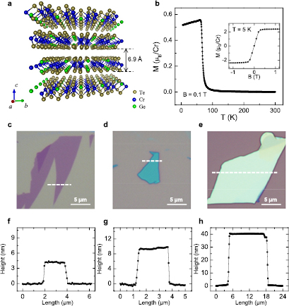
Figure 1. Preparation of the ferromagnetic 2D Cr2Ge2Te6 (CGT) from a single crystal. (a) Schematic drawing of the CGT's layered crystal structure along the (0 0 0 1) orientation. These layers are stacked together via the van der Waals interaction with an interlayer distance of ~6.9 Å. One monolayer CGT is ~6.9 Å thick, indicated by the black arrow. (b) The magnetization of CGT single crystal as a function of the temperature under a magnetic field of 0.1 T. The inset is the magnetic field dependence of the magnetization measured at 5 K. During the measurements, the magnetic field is applied parallel to the crystal's ab-plane. (c)–(e) The optical images of three typical 2D CGT flakes with different thicknesses. (f)–(h) The thicknesses of these three 2D CGT flakes determined from the AFM measurement (see supplementary figures S1(a)–(c)). These line cuts are measured along white dashed lines in the optical images shown in figures 1(c)—(e).
Download figure:
Standard image High-resolution imageUsing the heating-assisted mechanical exfoliation method [30], we are able to obtain the 2D CGT flakes of various thicknesses down to a few nanometers. Figures 1(c)–(e) show the optical images of three typical CGT flakes, in which a brighter color corresponds to a thicker film. The thicknesses of these flakes are determined by atomic force microscopy (AFM) using the tapping mode (see supplementary figures S1(a)–(c) (stacks.iop.org/TDM/4/024009/mmedia)). As shown in figures 1(f)–(h), the thicknesses for the CGT flakes are determined to be ~4.5 nm, ~8.5 nm, and ~40 nm respectively, through height averaging in the line cuts, which are indicted by white dashed lines in figures 1(c)–(e).
Ferromagnetic properties of thin Cr2Ge2Te6
The MOKE is utilized to characterize the ferromagnetic properties of the exfoliated 2D CGT flakes. Figures 2(a)–(d) show the magnetic field dependence of the Kerr rotation in arbitrary units for a ~40 nm CGT flake at 3, 20, 40, and 60 K, respectively, after the subtraction of a linear background and normalization. During the measurement, the magnetic field is applied parallel and in the plane of the 2D CGT flake using the longitudinal geometry. The inset of figure 2(a) shows the optical image of this ~40 nm flake and the red dot indicates the location of the laser spot. At 3 K, a pronounced magnetic hysteresis loop is observed, which unambiguously demonstrates the ferromagnetic property of the ~40 nm CGT flake. The mild yet distinguishable hysteresis loop of the Kerr rotation at 60 K indicates the Curie temperature is higher than 60 K, which is close to the bulk Curie temperature of ~61 K [28, 32]. This can be explained by the relative thick nature of this CGT flake. We are not able to obtain the MOKE hysteresis on ~20 nm CGT flake (see supplementary information S1 and figure S2). One possible reason is related to the limited sensitivity of our current MOKE setup (~1 micro radian), and the other possible cause is the oxidation of the surface layer of the 2D CGT. Since the monolayer CGT is predicted to be ferromagnetic with a Curie temperature of 106 K [33], the MOKE measurement on the thin CGT samples down to single layer requires future studies using high-resolution MOKE, such as Sagnac interferometer enhanced magneto-optic measurements that has a sensitivity of several nano radians and was previously used to probe the broken time reversal symmetry in superconducting Sr2RuO4 [34].

Figure 2. Magneto-optic Kerr effect measurement on a 2D CGT flake (thickness: ~40 nm). (a)–(d) The magnetic field dependence of the Kerr rotation on 2D CGT flake measured at 3, 20, 40, and 60 K, respectively, after the subtraction of a linear background and normalization. The red curves indicate the magnetic field swept from positive to negative, and the black curves indicate the magnetic field swept from negative to positive. The inset in (a) is the optical image of this 2D CGT flake, where the red dot indicates the location of the linearly polarized HeNe laser spot.
Download figure:
Standard image High-resolution imageElectric field effect of the thin Cr2Ge2Te6 flakes
One major advantage of the 2D materials is that their physical properties could be largely tuned via the modulation of the Fermi level by a perpendicular electric field [9, 31, 35]. To explore the electric field effect in the 2D CGT, we fabricate Hall-bar devices using the nanofabrication technique. To avoid degradation due to oxidation (see supplementary S2 and figure S3) [21], we tried to minimize the time that CGT is exposed in air during fabrication and the devices are measured in vacuum. Figure 3(a) shows the schematic of the device fabricated on the 2D CGT flakes on the SiO2/Si substrate, where the thickness of SiO2 is ~300 nm and the highly electron-doped Si is used as a back gate to provide the electric fields. Three representative devices fabricated on different thicknesses of CGT flakes are selected to describe the main results in our study. Device A, B, and C are fabricated on ~25 nm, ~15 nm, and ~12 nm CGT flakes, respectively, where the thicknesses are determined by AFM measurement after the electrical measurements. The channel resistances are obtained by the four-probe measurement in an Oxford Spectromag system. Figure 3(b) shows the typical voltage (Vxx) versus the current (I) measured at 300 K for Device A made on ~25 nm CGT (channel width/length: 1.7/2.5 µm) at the gate voltages of 80 V, 40 V, 0 V, −40 V, and −80 V, respectively. The gate voltage dependence of the channel resistances that are extracted from the slope of the Vxx versus I curves is summarized in figure 3(c). A more dramatic modulation of the channel resistances is observed on Device B with ~15 nm CGT (channel width/length: 1.2/1.5 µm; see supplementary figure S4), and Device C with ~12 nm CGT (channel width/length: 1.7/0.8 µm), as shown in figures 3(d) and (e). Figure 3(d) shows the typical Vxx versus I curves measured at 300 K for Device C at the gate voltages of 80 V, 40 V, 0 V, −40 V, and −80 V, respectively, and the channel resistance versus gate voltage is plotted in figure 3(e). The maximum resistance of 117 MΩ at Vg = 80 V is ~50 times larger than the lowest value of 2.2 MΩ at Vg = −100 V. This gating effect is much more profound in Device C compared to Device A. The universal feature of less gating effect in thicker CGT films is further confirmed by measurements on Device D (~29 nm) and E (~18 nm) (see supplementary information S3 and figure S5). For even thinner flakes less than ~8 nm, we have not been able to perform electrical measurements even under large gate voltages (see supplementary information S4 and figure S6), which we believe might be due to similar issues, including large contact resistances and oxidation during the fabrication process (See supplementary figure S3), which have been observed on semiconducting 2D materials, such as transition metal dichalcogenides [36–38].

Figure 3. Gate voltage tuning of the channel resistances of the 2D CGT devices at 300 K. (a) Schematic of the Hall bar devices fabricated on the 2D CGT flakes on the SiO2/Si substrate, where the n-doped Si is used as a back gate, the thickness of the SiO2 layer is 300 nm and Pt electrodes are used for electrical contacts. (b) The four-probe measurement of the channel resistances of Device A (CGT thickness: ~25 nm; channel width/length: 1.7/2.5 µm) at various gate voltages at 300 K. (c) The gate voltage dependence of the channel resistance for Device A at 300 K. (d) The four-probe measurement of the resistance of Device C (CGT thickness: ~12 nm; channel width/length: 1.7/0.8 µm) at various back gate voltages at 300 K. (e) The gate voltage dependence of the channel resistances of Device C at 300 K.
Download figure:
Standard image High-resolution imageThe channel resistances of these devices are measured as a function of temperature under different gate voltages (figures 4(a)–(c)). For Device A with ~25 nm CGT (figure 4(a)), the ungated device exhibits an semiconducting feature, which is consistent with our previous study on bulk CGT [28]. The gate tuning of the channel resistance shows the same trend as that at 300 K in the full temperature range, but the modulation is more dramatic at low temperatures. When the films become thinner, the channel resistances exhibit a large increase. For instance, at 300 K and Vg = 0 V (blue squares in figures 4(b) and (c)), Device B (~15 nm CGT) has a channel resistance of ~10 MΩ, and Device C (~12 nm CGT) shows channel resistance of ~130 MΩ. For Device B, the gate voltage modulation of the channel resistance is more profound compared to Device A. At 1.5 K, the ratio of maximum/minimum in channel resistance is ~70 for Device B, which is much larger compared to Device A. For even thinner flakes, a giant modulation of the channel resistance is observed. As shown in figure 4(c) for Device C, the channel resistance changes from very insulating (not measurable below 250 K) at 0 V to quite conducting, which shows a resistance of ~1.6 MΩ at −100 V and 1.5 K. At low temperatures, a non-linear feature of the Vxx versus I curves (figure S6) for thinner CGT devices could be associated with the hopping transport mechanism. The resistance values are obtained from the linearly fitted lines at the high bias region (see supplementary information S5 and figure S7). From the temperature dependence of the channel resistance, two major conclusions could be drawn. First, for the electrical properties of the CGT flakes, a clear thickness dependence is observed. As the thickness decreases, the resistivity increases, and the gate effect is more profound. This observation can be explained by the distribution of the induced charge carriers over the layers when the CGT is thicker. Second and most importantly, for thicker CGT Device A under −80 V, the channel resistance increases as the temperature decreases, still indicating a semiconducting feature, while for thinner CGT Device C, the channel resistance decreases as the temperature decreases under the gate voltage of −80 V and −100 V (figure 4(c) inset), indicting a metal-like behavior, in stark contrast to the semiconducting/insulating properties while ungated.

Figure 4. Large modulation of the channel resistances of the 2D CGT devices by electric field effect. (a)–(c), The temperature dependence of the channel resistances at various gate voltages for Device A (CGT thickness: ~25 nm; channel width/length: 1.7/2.5 µm), B (CGT thickness: ~15 nm; channel width/length: 1.2/1.5 µm), and C (CGT thickness: ~12 nm; channel width/length: 1.7/0.8 µm), respectively. Inset of (c): the temperature dependence of the channel resistances at −80 and −100 V, which exhibits metal-like behavior.
Download figure:
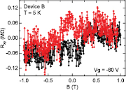
Standard image High-resolution imageThe magnetic properties of the gated devices are characterized by anomalous Hall effect in a magnetic field applied perpendicular to the device geometry. Figure 5 shows the measurement of the anomalous Hall resistance on Device B at −80 V and 5 K. A clear switching is observed at ~0.2 T when the magnetic field is swept from −1 T to 1 T (black line), and a sharp drop is observed at ~ −0.2 T while sweeping the magnetic field from 1 T to −1 T (red line). These two sharp switchings indicate the ferromagnetic properties of the 2D CGT when it is gated to be close to the ferromagnetic metallic region. The characterization of the ferromagnetic properties of the ungated devices based on anomalous Hall effect measurement is quite challenging due to the extremely resistive properties of CGT. Using bulk CGT for example, it is hard to get a clear signal even for ordinary Hall measurement when the CGT becomes quite insulating at low temperatures (see supplementary figure S8). The fully understanding of the electric field effect on the magnetic anisotropy and Curie temperature requires future studies on the same devices by both MOKE and AHE.
Figure 5. Anomalous Hall measurement on the gated 2D CGT device (Device B). The magnetic field dependence of the Hall resistance (Rxy) for gated Device B at −80 V and 5 K after the subtraction of a linear background. The red curve indicates the magnetic field swept from positive to negative, and the black curve indicates the magnetic field swept from negative to positive. The two large resistance changes at ~0.2 T and ~ −0.2 T are the signatures of the ferromagnetic properties of the gated Device B, and ~0.2 T corresponds to the coercive field of the gated 2D CGT.
Download figure:
Standard image High-resolution image
Conclusion
In summary, we have succeeded in the preparation of few-layer 2D CGT, which exhibits ferromagnetic properties below the Curie temperature, and in the gate voltage tuning of the channel resistances for the thin CGT devices. Our results could lead to the future studies on the electric field tuning of the ferromagnetic properties, such as Curie temperature, magnetic anisotropy, of the 2D ferromagnetic CGT, and on the van der Walls structures [8, 10, 27], such as CGT and graphene/topological insulator based Dirac materials for quantum anomalous Hall effect [32, 39]. Furthermore, the optimization of the isolation technique, such as sandwiched between two BN layers [8, 40–42], could yield a high quality single layer CGT, which is theoretically predicted to have a Curie temperature of 106 K [33].
Note added: during the review process of our manuscript, we noticed the identification of intrinsic long-range ferromagnetic order in pristine Cr2Ge2Te6 atomic layers down to 2 layers via Sagnac interferometer enhanced magneto-optic measurements by Gong et al [26].
Acknowledgments
We acknowledge the fruitful discussions with Professors Ji Feng, and Xi Lin. We acknowledge the financial support from National Basic Research Programs of China (973 program Grant Nos. 2015CB921104, 2014CB920902, 2013CB921901 and 2014CB239302) and National Natural Science Foundation of China (NSFC Grant No. 11574006). WH also acknowledges the support by the 1000 Talents Program for Young Scientists of China.