

Abstract
Nickel oxide (NiO) is a p-type metal-oxide semiconductor with wide-ranging applications. Recent studies have focused on the gas-sensing properties of this semiconductor. This study introduces an easy process for growing NiO nanowalls on a glass substrate using Ni foil and aqueous  . The morphology and structure of the NiO nanowalls are investigated and confirmed by field-emission scanning electron microscopy and x-ray diffraction (XRD) analyses. The gas-sensing properties of the prepared nanowalls are tested using a dynamic gas-testing system wherein the target gases are
  and
and  . Gas-sensing data show that the synthesized NiO nanowalls are highly responsive toward
  . Additionally, a sensing device prepared based on the NiO nanowalls is found to be stable during measurements, exhibiting a linear variation with changes in
  concentration.
Export citation and abstract BibTeX RIS

Original content from this work may be used under the terms of the Creative Commons Attribution 3.0 licence. Any further distribution of this work must maintain attribution to the author(s) and the title of the work, journal citation and DOI.
1. Introduction
Nickel oxide (NiO) is a  type semiconductor with a wide bandgap energy of 3.6–4.0 eV. NiO is a stable
  type metal oxide with high carrier transport performance [1, 2] and thus has wide-ranging applications, such as in lithium-ion batteries [3], supercapacitors [4], biosensors [5], and catalysts for water splitting [6]. Moreover, many groups claim that NiO nanomaterials exhibit excellent sensing properties toward formaldehyde,
  , ethanol,
  , and
, and  [1, 2, 7–9]. However, studies on the
  sensing behavior of NiO nanostructures are few.
NiO nanomaterials with wall-plate-like morphologies are predominantly synthesized [10–13] among others (e.g. nanorods, nanowires, nanoflowers, and nanotubes) [14–17]. Several groups introduce different approaches for the synthesis of NiO nanowalls on Ni metal surfaces. Zhan et al synthesized 3D NiO nanowalls on a Ni foam through a hydrothermal method [10]. Tang et al [13] used electrochemical corrosion approach to prepare NiO nanowalls grown on a Ni foam. Ni et al introduced an easy electrochemical corrosion method to fabricate NiO nanowalls [18]. NiO nanowalls can also be prepared by plasma-assisted oxidation [19]. Recently, our group introduced an easy, low-cost method of synthesizing  nanowalls through the surface reaction of Ni foil in aqueous
  [20]. Nonetheless, the gas-sensing properties of the NiO nanowalls fabricated by these methods remain lacking. The advantage of NiO nanowalls over other morphologies like nanowire, nanoparticles or nanosheets is to provide better film porosity which can enhance the adsorption and desorption processes of the target gases over the film surface.
In this study,  nanowalls were fabricated through the chemical reaction of Ni foil with aqueous
  . The NiO nanowalls were obtained by dehydrating the
  nanowalls at
  using a hotplate. The
  and
and  sensing properties of the as-prepared NiO nanowalls were investigated and compared at a working temperature of
  .
.
2. Experimental details
We used a facile method in our previous study to synthesize the NiO nanowalls using a Ni foil [20]. Figure 1 illustrates our synthesis process. Commercial pure Ni foil (thickness  ; purity = 99.99%; Aldrich) was cut into a
  plate (figure 1(a)). The plate was immersed in acetic acid for 10 min and then ultrasonically cleaned in a bath sonicator with acetone, ethanol, and distilled water for 5 min. After drying under a flow of
  , the plate was folded at the corners to form table-like plate and was added to 25 ml of
  solution in a 100 ml Duran laboratory bottle (figure 1(b)). Meanwhile, a cleaned glass (
 ) was positioned under the plate. The Duran bottle was kept at
  for 48 h in an oven. After treatment, the glass substrate was covered by a green film (figure 1(c)), dried in an oven at
  for 12 h, and annealed at
  for 1 h using a hotplate. As a result, the green film became a dark brown film (figure 1(d)). A simple parallel Au electrode was patterned on the film by thermal evaporation (figure 1(e)).

Figure 1. Experimental process model. (a) Ni foil, (b) Ni foil and glass substrate treated in  , (c) glass substrate after treatment, (d) glass substrate after annealing at 500 °C for 1 h, and (e) Au electrode patterned on the annealed substrate.
Download figure:
Standard image High-resolution imageThe morphologies of samples were characterized by field-emission scanning electron microscopy (FESEM; JEOL JSM-7610F). The structures of the samples were identified using x-ray diffraction (XRD; XPERT-PRO) with Cu Kα radiation of  . The NiO nanomaterial was extracted from the annealed sample and was dispersed on a molybdenum grid for transmission electron microscopy (TEM; Philips Telnai G2F20 S-TWIN) observations. The gas-sensing properties of the as-synthesized materials were measured using a dynamic gas-testing system. During measurement, the chamber was pumped and was maintained at a vacuum pressure of 10 Torr. The carrier gas was dry air and the total flux rate was 200 sccm. The operating temperature was from
  to
to  (
( is the maximum value of our gas-testing system). Gas response was defined as
  , where
  and
and  represent sensor resistance in the target gas and air, respectively. Sensor response
  and recovery time
  are determined by the time for sensor resistance to reach 90% of its steady-state value from
  to
to  and
and  to
to  , respectively.
3. Results and discussion
Figure 2 shows the XRD patterns of the films before and after annealing at  . For the pristine film, major diffraction peaks at
  and
and  can be assigned to the (001), (110), (111), and (301) planes of
  [JCPDS file no. 00-022-0444, hexagonal structure, space group P–31 m (162)] (figure 2(a)). Minor peaks at
  values of
  and
and  correspond to (001), (100), and (103) planes of
  [JCPDS file no. 00-014-0117, hexagonal structure, space group P–31 m (164)]. No other impurities form in the film. Figure 2(b) shows the XRD pattern of the annealed film, indicating that
  was transformed to NiO. The peaks located at
  and
and  well agree with (101), (012), and (110) planes of NiO [JCPDS file no. 98-016-6115, hexagonal structure, space group R–3 m (166)]. In this pattern, the second phase of
  [JCPDS file no. 00-006-0144, hexagonal structure] is also detected by the existence of (100), (006), and (105) planes at the diffraction peaks of
  and
and  , respectively. The board peaks observed in both patterns suggest that the film is composed of small crystallites. The crystallite size of NiO calculated through the Scherrer equation [21] with the
  of
of  is 2.2 nm.

Figure 2. XRD patterns of the treated glass substrate (a) before and (b) after annealing at 500 °C for 1 h.
Download figure:
Standard image High-resolution imageThe surface morphologies of the film before and after annealing at  for 1 h were similar (figures 3(a) and (c)). The films comprise curvy nanowalls with an average thickness of 15 nm. Cross-sectional FESEM images indicated that the thickness of both films is ~1450 nm (figures 3(b) and (d)). The sample before annealing (figure 3(b)) comprises a film layer (~314 nm) and a nanowall layer (~1122 nm). The sample after annealing is dense with a nanowall thickness of approximately 561 nm (figure 3(d)). The synthesis of NiO nanowalls, in which Ni can react with
  to form
  , which was dispersed in the solution, was proposed in our previous study [20]. The nanowalls are probably formed by an oriented assembly of
  units onto the
  nanoseeds. The transformation from
  to NiO without morphology change at
  is well documented [20, 22, 23].

Figure 3. Top view and cross-sectional FESEM image of the treated glass substrate (a) and (b) before and (c) and (d) after annealing at |500 °C for 1 h. The scale bar is 100 nm.
Download figure:
Standard image High-resolution imageFigures 4(a) and (b) show the TEM and HR-TEM images of the extracted NiO nanowalls, respectively. The nanowalls were composed of many small crystallites (figure 4(b)). The dimensions of all crystallites are analyzed in a histogram graph (figure 4(c)). The average diameter of the crystallites is 2.2 nm, which is similar to the calculated value using the XRD pattern equation above.

Figure 4. (a) TEM and (b) HR-TEM images of the sample annealed at 500 °C for 1 h. (c) Size distribution of the crystallites in figure (b).
Download figure:
Standard image High-resolution imageFigure 5 shows the gas responses of the as-prepared NiO nanowalls toward  and
and  . The device is highly sensitive to
  . The
. The  response of the device gradually increases from 6.3% at
  to 8.7% at
  and saturates to 8.8% at
  . The optimal operating temperature of the NiO nanowalls was
  to
to  and
and  and
and  to
to  . Figure A1 (appendix) shows the transient curves of the device at different operating temperatures. The positive response of the device to reduced gases (
 and
and  ) and to oxidizing gas
  suggests that the NiO nanowalls exhibit a
  type semiconductor sensing characteristic. The gas-sensing mechanisms of NiO to both types of gases are well documented [7, 24]. Table 1 shows a comparison of NiO nanowall-based
  sensor with other materials. The sensing performance, 'gas response' and 'response/recovery time' of the synthesized NiO nanowalls are not better than those of reported nanomaterials. However, the sensing performance of a gas sensor strongly depends on many factors, such as electrodes (material, gap, size, shape, and position), testing system set-up (gas inlet position and flux rate), and test chamber (chamber volume, medium with/without oxygen, and humidity). Thus, the limit of detection (LOD) to
  should be considered for comparison. For this specification, the NiO nanowalls can detect down to 1 ppm
  gas, which is better than many of the reported
  sensors.
Table 1. Comparison of NiO nanowall-based  sensor and other reported
  sensors.
| Material | Operating temperature (°C) |  concentration (ppm) concentration (ppm) |
Gas response | Response time (s) | Recovery time (s) | LOD | Ref. |
|---|---|---|---|---|---|---|---|
| BiFeO3 nanoparticles | 300 | 5 | 2.03 | 20 | 50 | 5 ppm | [25] |
Graphene oxide +  nanocomposites nanocomposites |
60 | 10 | 1.25 | ~150 | ~150 | 10 ppm | [26] |
 nanocomposites nanocomposites |
350 | 5 | ~10 % | 60 | 360 | 5 ppm | [27] |
 nanotubes nanotubes |
200 | 10 | ~15 % | ~100 | ~100 | 10 ppm | [28] |
 thin film thin film |
180 | 500 | 55 | 80 | 70 | 50 ppm | [29] |
 nanoparticles nanoparticles |
260 | 5 | ~1.18 | ~180 | ~600 | 5 ppm | [30] |
 nano-dodecahedrons nano-dodecahedrons |
183 | 5 | 1.5 | ~10 | ~15 | 200 ppb | [31] |
| NiO nanowalls | 300 | 5 | 4 % | 40 | 57 | 1 ppm | This work |

Figure 5. Influence of operating temperature  on the sensor response after exposure to
  and
and  .
.
Download figure:
Standard image High-resolution imageThe  sensing behavior of the NiO nanowalls is related to the reaction of the adsorbed oxygen adatoms
  on the NiO surface with the
  molecules, which can be described as equation (1):

After the reaction, the reduced number of holes in the accumulation zone results in increased sensor resistance. The sample exhibits higher response toward  than toward
  although both gases possessed sulfide in the molecules. This behavior can be attributed to the reaction of
  with NiO as mentioned by Tyagi et al [31]. NiO can react with
  gas to produce NiS:

The produced  gas molecules react with the remaining oxygen adatoms on the NiO surface:

Under the presence of oxygen, NiS can be transformed to NiO:
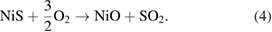
The released  in equations (3) and (4) further reacts with oxygen adatoms following equation (1), thereby decreasing the number of holes in the accumulation. Thus, the NiO nanowalls are more sensitive to
  than to
  .
.
Studies on the gas-sensing behavior of  are rare. However,
  remained in the sample after annealing. This phase is possibly remained at the bottom of the sample because of the thick/dense film.
  can be easily transformed to NiO by giving off water molecules above
  [32]. The decomposition of
  may be prohibited at the bottom of the film because the film was thick and dense. Thus, the
  layer may not influence the sensor performance during the test.
Device stability is confirmed by the transient curves after exposure to 5 pulses of 20 ppm  (figure 6(a)). Sensor resistances under 'gas on' and 'gas off' are retained. At
  operating temperature, the response and recovery times of the device to 20 ppm
  are 40 and 57 s, respectively (figure 6(b)). Figure 7 reveals the influence of
  concentration on sensor resistance and sensor response. The minimum
  concentration that the device can detect is 1 ppm (figure 7(a)) with a response of just above 2.5%. The relationship of the increase in sensor response with
  concentration is linear (figure 7(b)). The linear correlation coefficient
  is 99%, indicating the high potential of the as-synthesized nanomaterial as a
  sensor.

Figure 6. Gas response/recovery curve of NiO nanowalls to 20 ppm  at 300 °C after (a) five-cycle and (b) one-cycle pulses.
Download figure:
Standard image High-resolution image
Figure 7. Influence of  concentration (from 20 ppm to 1 ppm) on (a) sensor resistance and (b) sensor response with fitted equation.
Download figure:
Standard image High-resolution image4. Conclusions
Curvy NiO nanowalls were grown on a glass substrate through the reaction of Ni foil in aqueous  . The nanowalls are found to be uniform with an average thickness of 15 nm. The nanowalls are extremely sensitive to
  compared with
  and
and  . The highest response of the device to
  is 8.8% at
  , and this value is approximately two, six, and two times higher than the responses of the device to
  and
and  , respectively. The as-prepared NiO nanowalls exhibit good stability (in terms of sensor resistance), reasonable response/recovery time (below 1 min), and linear variation of resistance with
  concentration. The LOD of the NiO nanowalls to
  is 1 ppm. Thus, the NiO nanowalls synthesized through our simple method are a high-potential
  sensor.
Acknowledgments
This research is funded by the Vietnam National Foundation for Science and Technology Development (NAFOSTED), under grant number 103.02-2016.20.
Appendix

Figure A1. Response versus recovery curves of the NiO nanowalls toward  and
and  at the operating temperature of
  (a),
(a),  (b),
(b),  (c),
(c),  (d),
(d),  (e), and
  (f).
(f).
Download figure:
Standard image High-resolution image