

Abstract
In this work BixTey thin films were deposited on polyimide substrate by a high-pressure RF magnetron sputtering technique. The deposited condition was maintained using a high pressure of 1.3 × 10⁻² mbar. The as-deposited films show Bi2Te3 structure with Te excess phase (Te-rich Bi2Te3). After that, as-deposited films were annealed in the vacuum chamber under the N2 flow at temperatures from 250 to 400 °C for one hour. The microstructure, cross-section, [Bi]:[Te] content, and the mechanical, electrical and thermoelectric properties of as-deposited and different annealed films were investigated. It was found that the annealing temperature enhanced the crystallinity and film density for the temperature range 250–300 °C. However, the crystal structure of Bi2Te3 almost changed to the BiTe structure after annealing the films above 350 °C, due to the re-evaporation of Te. Nano-indentation results and cross-section images indicated that the hardness of the films related to the film density. The maximum hardness of 2.30 GPa was observed by annealing the films at 300 °C. As a result of an improvement in crystallinity and phase changes, the highest power factor of 11.45 × 10⁻⁴ W m−1K−2 at 300 °C with the carrier concentration and mobility of 6.15 × 1020 cm−3 and 34.03 cm2 V−1 s−1, respectively, was achieved for the films annealed at 400 °C.
Export citation and abstract BibTeX RIS

Original content from this work may be used under the terms of the Creative Commons Attribution 3.0 licence. Any further distribution of this work must maintain attribution to the author(s) and the title of the work, journal citation and DOI.
1. Introduction
Bismuth telluride (Bi2Te3) compound is known as one of the best thermoelectric materials because it has a relatively high figure of merit at room temperature. Figure of merit (ZT) is defined as ZT = S2 σT/K, where S is the Seebeck coefficient (V K−1), σ is electrical conductivity (S m−1), K is thermal conductivity (W m−1K−1) and T is absolute temperature (K). In general, S is inversely proportional to the carrier concentration, while σ is directly proportional to the carrier concentration. S and σ values cannot increase together because of the influences of the quantum confinement effect and the electrical transport property effect on nanostructured materials [1]. Low-dimensional thermoelectric thin film has been proposed in order to achieve less thermal conductivity (K ) and increase the ZT value. Thermoelectric thin film is a low-dimensional system that gives a lower dimensional scale than the bulk phase [2–8]. From the literature reviews, there are several techniques to prepare Bi2Te3 thin films, such as thermal evaporation [3], metal organic chemical vapor deposition (MOCVD) [4], molecular beam epitaxy (MBE) [5], pulsed laser deposition (PLD) [6], RF magnetron sputtering [7, 9, 10] and electrochemical deposition [8]. Among them, RF magnetron sputtering would be an appropriate technique because it has obtained high-quality thin film and it is more easily extended on a large scale [7, 11]. In addition, flexible thermoelectric modules have attracted attention in recent years because they are effective when applied to various heat sources [3, 12].
The annealing process is a material treatment method used in semiconductor processing. It has been reported that the annealing process has positive effects on the structural, electrical and thermoelectric properties of Bi2Te3 [10, 13–15]. However, the problem is the loss of Te in the annealed thin films as the annealing temperature increases. It causes the re-evaporation of the volatile Te elements during the annealing process [15]. Therefore, it is difficult to control the stoichiometric Bi2Te3 phase ([Bi]:[Te] = 2:3) in the annealing process. For this reason, the as-deposited film should be prepared as Te-rich Bi2Te3. The composition of the films can be controlled by adjusting the deposition pressure in RF magnetron sputtering [16]. As-deposited Te-rich Bi2Te3 thin films were prepared by a high pressure RF magnetron sputtering technique. The annealing temperature is a key parameter to achieve thermoelectric performance. In this work RF magnetron sputtering from an alloy Bi2Te3 target was used while co-sputtering technique of dual targets: Bi and Te targets was investigated in previous works [7, 9, 10]. Our method is remarkably simpler than that in previous work.
It is also known, on the actual application, that contact loading during processing and/or packaging degrades the performance of the device. Consequently, the successful fabrication of devices based on Bi2Te3 thin film also required significant study and understanding of the mechanical properties. Therefore the study of mechanical properties on thermoelectric material is crucial. Most research has been focused on the thermoelectric properties of Bi2Te3 thin films, but there has only been a small amount of research done on mechanical properties. Tasi et al [17] studied the mechanical properties of Bi2Te3 prepared by pulse laser deposition (PLD) under various helium gas pressures on sapphire substrates. He found that the hardness and Young's modulus depend on helium gas pressure. The hardness and Young's modulus were found from 2.92 to 4.02 GPa, and 106.31 to 127.46 GPa, respectively. However, the effect of annealing temperature on mechanical property of Bi2Te3 films deposited on flexible polymer substrate has not been investigated.
A high pressure RF magnetron sputtering technique was selected for this research to fabricate Te-rich Bi2Te3 thin film on a flexible polyimide Kapton® substrate. Polyimide has low thermal conductivity around 0.12 W mK−1 and is stable at temperatures below 400 °C. This polymer also has a thermal expansion coefficient similar to Bi2Te3 [3, 18]. The as-deposited films were annealed at the temperature range of 250 to 400 °C under N2 atmosphere. The effects of the annealing temperature on the structural, mechanical and electrical properties were investigated.
2. Experimental
Bismuth telluride thin films were deposited on polyimide substrate by RF magnetron sputtering from the Bi2Te3 target (99.9%) with a diameter of three inches. The distance between the target and the substrate was about 50 mm. The polyimide substrates were ultrasonically cleaned in ethanol for 15 min. The sputtering condition was kept at an RF power of 45 W, working pressure of 1.3 × 10⁻² mbar with Ar as the sputtering gas, and a deposition time of 30 min. Before the deposition process, the base pressure of the deposition chamber was 2 × 10⁻⁵ mbar. After that, the as-deposited films were annealed at different temperatures (250, 300, 350 and 400 °C) for one hour under N2 atmosphere. The microstructure, chemical composition, cross-section, and mechanical, electrical and thermoelectric properties of as-deposited and various annealed films were characterized by x-ray diffraction (XRD, Bruker-D8-Discover)/Raman spectroscopy (XploRA PLUS), a field emission scanning electron microscope (FE-SEM, JSM-7001F)/energy dispersive x-ray spectrometer (EDS), nano-indentation (NHT2 CSM Instrument), Hall effect measurement (Ecopia HMS-3000), and a DC four-terminal method (ZEM-3, ULVAC-RIKO), respectively.
3. Results and discussion
3.1. Structural properties of as-deposited and different annealed films
[Bi]:[Te] of bismuth telluride thin films at different annealing temperatures were analyzed by EDS and the Te content (%) is shown in figure 1. From the EDS result, the Te content of the as-deposited film was about 64 at.% (Te rich). The reason that as-deposited film is Te rich can be explained by the effect of the high deposition pressure.
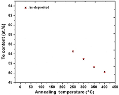
Figure 1. Illustrates the Te content in bismuth telluride thin film at different annealed temperatures.
Download figure:
Standard image High-resolution imageAt a high deposition pressure, the density of gas in the deposited system will be relatively high. Ar+ will interrupt the path of Bi atoms, which are bigger than Te atoms (Bi = 143 pm, Te = 123 pm [19]), making them to fall down to the substrate and causing the composition of Bi atoms to be less than the composition of the target (Bi2Te3). When the films were annealed at the temperature range of 250–400 °C, Te atoms evaporated during the annealing process and caused a content of decreasing Te. According to the crystal structure of Bi2Te3, it consists of five-layer units of Bi and Te hexagonal planes, stacked along the c-axis with atomic order Te(1)–Bi–Te(2)–Bi–Te(1) and the layer Te(1)–Te(1),that are weakly bonded together by the Van der Waals force [20]. In conclusion, with the increase of the annealing temperature, the volatile Te elements occur during the annealing process [15].
XRD patterns of as-deposited and different annealed films are shown in figure 2. From figure 2(a), the XRD results indicate that the as-deposited film can be attributed to the rhombohedral Bi2Te3 structure (JCPDS 15-0863) and the Te structure found at the (1 1 2) plane (JCPDS 44-0925). Figures 2(b) and (c) are XRD patterns of the films annealed at 250 °C and 300 °C, respectively. It was seen that their intensities and peak positions had obviously changed. It is clear that the peak of the (1 1 2) plane in the Te phase reduces at high temperatures. This result indicated that Te atoms decrease as the annealing temperature increases. When the films were annealed at the temperature of 350 °C and 400 °C (figures 2(d) and (e)) a hexagonal BiTe structure was found (JCPDS 75-1095) with the preferred orientation of (1 0 4). It reveals that the annealing process enhances the crystallinity and changes the crystal structure of the films [9, 10, 15]. The sharpest intensity peaks of the films were also found at an annealing temperature up to 400 °C, as seen in figure 2(e). The crystal size of the films was calculated using the Debye–Scherrer equation
where k = 0.9, λ is the wavelength of Cu-Kα = 0.154 nm, β is the full-width-half-maximum, and θ is the diffraction angle. The results show that the crystal sizes increased from 3.24 to 39.64 nm with the increase in the annealing temperature.
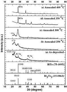
Figure 2. XRD patterns of bismuth telluride films annealed at different temperatures. (a) As-deposited. (b) Annealed 250 °C. (c) Annealed 300 °C. (d) Annealed 350 °C. (e) Annealed 400 °C.
Download figure:
Standard image High-resolution imageRaman spectra of bismuth telluride films were acquired in a back scattering configuration, equipped with a frequency-double Ng: YAG 532 nm laser, as shown in figure 3. Raman spectra of as-deposited films were found at Raman wavenumbers at 102, 117 and 133 cm−1. The wavenumbers at 102 and 133 cm−1 were namely  and
and  , aligned with a Bi2Te3 vibration patterns mode reported by Russo et al [21], while the wavenumber at 117 cm−1 referred to A1g of the Te vibration pattern. In addition, the Raman spectra trended to shift towards the lower wavenumber (blue shift) when the annealing temperature was increased. Analysis of the Raman spectra of bismuth telluride films was supported by EDS and XRD measurements.
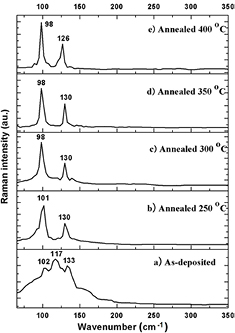
Figure 3. Raman spectra of bismuth telluride films annealed at different temperatures. (a) As-deposited. (b) Annealed 250 °C. (c) Annealed 300 °C. (d) Annealed 350 °C. (e) Annealed 400 °C.
Download figure:
Standard image High-resolution imageFigures 4(a)–(e) and 5(a)–(e) show the surface and cross-section SEM images of as-deposited and annealed films at temperatures of 250, 300, 350 and 400 °C, respectively. The bismuth telluride films annealed at temperatures of 250 and 300 °C (figures 4(b) and (c)) had smoother surfaces than the as-deposited film (figure 4(a)) as well as the films annealed at 350 and 400 °C (figures 4(d) and (e)). Therefore, this result indicated that the temperature range from 250 to 300 °C was available for surface improvement. The cross-sectional images revealed the thickness of the films in the range of 1.50 to 1.65 µm. As compared with the cross sections in figures 5(a)–(c), it is clear that the films annealed at 250 and 300 °C have higher density than the as-deposited film. For high annealing temperatures above 350 °C, films have a lower density than the as-deposited films, due to the re-evaporation of Te in the films. From SEM results, the increase in roughness and the reduction indensity of the films were found at annealing temperatures above 350 °C.
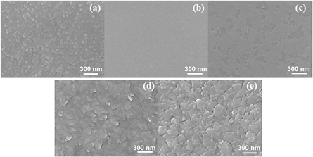
Figure 4. SEM images of (a) as-deposited; then showing it annealed at different temperatures: (b) 250 °C, (c) 300 °C, (d) 350 °C and (e) 400 °C.
Download figure:
Standard image High-resolution image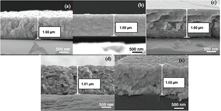
Figure 5. Cross-section of (a) as-deposited; then showing it annealed at different temperatures: (b) 250 °C, (c) 300 °C, (d) 350 °C and (e) 400 °C.
Download figure:
Standard image High-resolution image3.2. Mechanical properties of as-deposited and annealed films
The hardness of the as-deposited and annealed films measured at room temperature are shown in figure 6. The hardness of the as-deposited film is 1.89 GPa and it increases to 2.30 GPa at the annealing temperature of 300 °C. However, with films annealed at 350 to 400 °C, the hardness decreased to 1.58 and 1.10 GPa, respectively. This result corresponds to the density of film as seen from the cross-section images (figure 5). The hardness of Bi2Te3 depends on the conditions and deposition process. The hardness of Bi2Te3 prepared sputtering process has the value in arange between 1.46–2.91 GPa, and that will be even higher when using a PLD technique when itcan go up to 2.92–4.02 GPa [17]. Our result will be important for understanding the structural and nano-mechanical properties of bismuth telluride thin films prepared by a sputtering process.
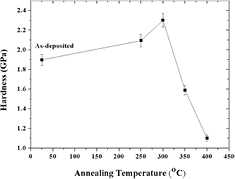
Figure 6. The relationship of the hardness of bismuth telluride thin film as a function of the annealing temperature.
Download figure:
Standard image High-resolution image3.3. Electrical and thermoelectric properties
The Seebeck coefficient (S) and carrier concentration (n) at room temperature were measured and the results are shown in figure 7. The S of all the samples exhibits negative values, indicating an n-type semiconductor of which electrons are the majority of the carriers. The film annealed at a temperature of 300 °C has the highest Seebeck coefficient of 71.41 µV K−1 and has the lowest carrier concentration of 2.27 × 1019 cm−3.

Figure 7. Seebeck coefficient and carrier concentration of bismuth telluride films at room temperature.
Download figure:
Standard image High-resolution imageIn general, the carrier concentration depends on defects in the films. When the films were annealed at temperatures of 250 to 300 °C, the Te concentration decreased due to volatilization and caused the generation of Te vacancy ( ). Subsequently, the antisite defect (
 ) and Bi vacancy (
 ) are produced as the Bi atom enters Te vacancies. This process can be described as [22]:

where  is the produced hole and ↑ denotes the volatilization of Te. From equation (2), we can see that the hole is generated by the volatilization of Te, and the carrier concentration of n-type Bi2Te3 can be reduced by the compensation of holes. On the contrary, the films annealed at temperatures of 350–400 °C exhibited an increase of carrier concentration from 2.43 × 10²⁰ to 6.15 × 1020 cm−3, respectively. It caused the structure to change from Bi2Te3 to BiTe. This result also corresponds to the research of Caha et al [23] which revealed that the free carrier concentration in BiTe is about 20 times larger than Bi2Te3. In addition, the S is decreased while the carrier concentration is increased. According to the simple theory for nearly free electrons [13, 24], the S can be shown by the following equation
where kB and h are Boltzman and Planck constants, respectively. m*, n and T are the effective mass of the carriers, carrier concentration and absolute temperature, respectively. Finally, R is a function of scattering. From equation (3) we conclude that S is directly proportional to T and inversely proportional to n2/3.
From figure 8, the crystal size and mobility of as-deposited and annealed films were calculated and measured at room temperature. With the increase in annealing temperature, the mobility and crystal size also increased. Large crystal sizes have a long effective mean free path of carriers and cause a reduction ingrain boundary and scattering center. The bismuth telluride film annealed at a temperature of 400 °C has the highest mobility of 34.03 cm2 V−1 s−1, and this was relatively close to the research of Zheng et al [13].

Figure 8. The crystal size and mobility of the as-deposited and differently annealed films.
Download figure:
Standard image High-resolution imageFigure 9 shows the Seebeck coefficient of bismuth telluride films as a function of measured temperature from 50 to 300 °C. The highest Seebeck coefficient (S) was observed on the film annealed at 300 °C. According to equation (3), S directly depends on the measuring temperature (T) and inversely depends on the carrier concentration (n). As the temperature increases, it not only affects the increase of S but it also increases the carrier concentration. The increase of S as the measuring temperature increased was found for the as-deposited film and annealed films at 350 and 400 °C. The films had a high carrier concentration in the order of 1020 cm−3. The increase of temperature slightly affected the carrier density. However, the films annealed at 250 and 300 °C with a lower carrier density had a similar Seebeck coefficient as the measuring temperature increased. This may cause a greater increase in carrier concentration and result in a reduction of the Seebeck coefficient.
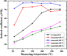
Figure 9. Temperature dependence of the Seebeck coefficient of bismuth telluride films annealed at different temperatures.
Download figure:
Standard image High-resolution imageFigure 10 shows the electrical conductivity (σ) of bismuth telluride annealed at different temperatures. The results show that σ of the films annealed at 350–400 °C is higher than the as-deposited and annealed films at 250–300 °C. The increase in electrical conductivity is due to the enhancement of the crystal size and defects in the films that led to increased mobility and carrier concentration. The film annealed at 400 °C had the highest electrical conductivity of 50 × 104 S m−1 at the measured temperature of 200 °C.
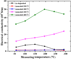
Figure 10. Temperature dependence of the electrical conductivity of bismuth telluride films annealed at different temperatures.
Download figure:
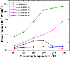
Standard image High-resolution imageFigure 11 shows the power factor (PF) of bismuth telluride films annealed at different temperatures. PF is a property of material able to generate more energy from temperature difference; it can be calculated by using the Seebeck coefficient and electrical conductivity (S2σ) under a given temperature. It was found that as-deposited films and those annealed at temperatures below 300 °C have a power factor in the range of 2.57 × 10⁻⁴ W m−1K−2. This value is close to the research of Huang et al [10] who reported that Bi2Te3 thin film annealed at 300 °C has the highest power factor of 4 × 10⁻⁴ W m−1K−2. The film annealed at 350 °C has a PF value of 7.49 × 10⁻⁴ W m−1K−2 at the measuring temperature of 300 °C. The film annealed at 400 °C has a maximum PF value of 11.45 × 10⁻⁴ W m−1K−2 with the highest electrical conductivity even though it had the lowest Seebeck coefficient. Compared to various deposition methods for bismuth telluride base thin film, the PF value of high pressure RF magnetron sputtered thin film obtained similar performances to those deposited by another technology. This implies that high pressure RF magnetron techniques following an annealing process can be used to prepare high performance bismuth telluride thin film.
Figure 11. Power factor of bismuth telluride films annealed at different temperatures.
Download figure:
Standard image High-resolution image
4. Conclusion
As-deposited Te-rich Bi2Te3 thin films were prepared by a high pressure RF magnetron sputtering technique. The annealing temperature ranges related to the variation of crystal structure, hardness, and the electrical and thermoelectric properties of as-deposited films. The annealing process caused the vaporization of Te and led to reduced Te-rich content. Crystallinity and crystal size were improved after the annealing process. For the annealed films at temperatures in the range of 250–300 °C, the film density was improved. The maximum hardness of 2.30 GPa was observed by annealing the films at 300 °C. The mobility of the films was increased with the increase incrystal size. For the temperature range above 350 °C, we found a phase change from Bi2Te3 to BiTe and the enhancement of carrier concentration with a decrease in the Seebeck coefficient. The maximum carrier concentration and mobility obtained by annealing the films at 400 °C were 6.15 × 1020 cm−3 and 34.03 cm2 V−1 s−1, respectively. The highest power factor of 11.45 × 10⁻⁴ W m−1K−2 was achieved for the annealed film at 400 °C.
Acknowledgments
The author would like to acknowledge the Faculty of Science, King Mongkut's Institute of Technology Ladkrabang for financial support. The author would like to thank National Electronics and Computer Technology Center, National Science and Technology Development Agency, Thailand for the Hall effect measurement.
Footnotes
- *
Contribution at the 4th Southeast Asia Conference on Thermoelectrics 2016 (SACT 2016), 15–18 December 2016, Da Nang City, Vietnam.