

Abstract
This paper presents the entire fabrication process including photolithography, sputtering, deep reactive ion etching (Bosch DRIE process) on silicon substrate and bonding process between the lid and silicon substrate to create a designed filtration microfluidic chip with dimension of 28 mm × 7 mm, one inlet port and one outlet port. A pattered silver thin film was deposited on a silicon sample by the lift-off method. Subsequently the newly fabricated sample was anisotropically etched by Bosch DRIE process. Some parameters of Bosch DRIE process such as bias power, duration of etching step and passivation step, oxygen presence were studied to explore the dependence of silicon channel depth and etched shape profile on these parameters. An optimized process was utilized to fabricate a featured silicon channel with vertical, smooth sidewalls and an overall good uniformity. The silicon channel has four arrays of microposts with various distances between microposts from 25 μm to 100 μm. The depth of the silicon channel was about 150 μm. After that, silicon substrate was bonded with mica lid by adhesive bonding method to form the completed filtration microfluidic chip. The samples were characterized by scanning electron microscopy (SEM), mechanical profilometer (DEKTAK 6 M), optical microscopy (Olympus MX51). In this paper a test was performed to demonstrate how the microfluidic chip works by pumping solution with many various sizes of particles through the inlet port of the microfluidic chip and obtaining a solution with desired particles sizes (smaller than 25 μm) through another port. Moreover, the chip could be pumped de-ionized water through outlet port for backwash in order to make this microfluidic chip reusable. Finally, a few applications of microfluidic chips are presented to illustrate the advantages of this technology and the potential for future development.
Export citation and abstract BibTeX RIS

Original content from this work may be used under the terms of the Creative Commons Attribution 3.0 licence. Any further distribution of this work must maintain attribution to the author(s) and the title of the work, journal citation and DOI.
1. Introduction
A microfluidic chip is a component device including one or more microfluidic channel in the micrometer scale. It is used to control and to manipulate the flow of small fluidic volume (μl, nl...) [1, 2]. Microfluidic systems may consist of pumps, mixing chamber, valves, etc, in order to help to control the flow of liquid which depends on many different factors such as the surface tension of liquid, capillary forces or viscosity [2]. Besides, fluid flow through microfluidic chip is laminar flow due to its low Reynolds number which is a non-dimensional parameter being the ratio of inertial force to viscous force and is determined by equation [2, 3]

where ρ, μ are the density and the viscosity of fluid and u, lc are the average velocity and characteristic length of the flow, respectively. If Reynolds number is less than 2300, the flow can be considered as laminar flow. Because microfluidic chip has dimension in micrometer scale, the average velocity and characteristic length of flow have small value, leading to small Reynolds number. The laminar flow has advantage of easier control and manipulation than turbulent flow.
Nowadays microfluidic systems attract significant scientific interest because they can control the fluid more precisely than conventional systems. Moreover, microfluidic chip is usually fabricated by using micro-electro-mechanical systems (MEMS) manufacturing technology which is suitable for the mass production. Besides that, the microfluidic chip only uses small volume of sample or reagent, leading to advantage of low cost analysis. According to many advantages of microfluidic chip such as laminar flow, small volume of sample and reagent, high surface-to-volume ratio, ability of mass production etc microfluidic chips have been applied in many different fields of physics, biology, chemistry such as applications in inkjet printing technology, filtering, cell sorting, cell capture, biochemical analysis, mixer, chemical synthesis, deoxyribonucleic acid (DNA) extraction etc [1–10].
Many materials can be used for fabrication of microfluidic chip and with each type of material, many appropriate fabrication processes can be applied [4]. At first, silicon and glass were selected as the substrate for microfluidic devices due to their ability of mass production by MEMS technology [11–13]. Recently, many type of polymers such as poly-dimethylsiloxane (PDMS), polymethyl methacrylate (PMMA), polyurethane methacrylate (PUMA)... were utilized as substrate materials for microfluidic chip replacing for silicon and glass due to their low cost and rapid fabrication [4, 6, 14, 15]. However, polymer-based microfluidic devices also have many disadvantages such as low chemical compatibility with many organic solvents, difficult fabrication of high aspect ratio micro and nanometer-scale structures [1, 4, 6, 7, 14, 15]. Therefore, silicon and glass microfluidic devices, on which high aspect ratio structures with high chemical compatibility can be fabricated by MEMS manufacturing technology, are still applied in many research fields [3, 5–7, 16, 17]. In recent years there has been a focus in using paper as substrate for microfluidic devices because of its low cost and hydrophilic property [4, 8, 18–20]. Besides that, paper-based microfluidic chip has many other advantages such as simple to use, easy to be fabricated by inkjet printing or cut-and-stack method [18–20]. However, drawbacks of paper substrate are obvious such as not suitable for liquids with low surface tension, difficult for high-density integration and uneasy to control the evaporation of liquid to open channels [4]. Therefore, silicon substrate is still the promising candidate to obtain stable microfluidic chip instead of polymer or paper.
Bosch DRIE is the highly anisotropic dry etching process combining two steps, passivation step and etching step, in order to create vertical sidewall feature on silicon substrate with high aspect ratio. In the passivation step, the precursor gas, octafluorocyclobutane (C4F8), allows depositing a passivation layer of fluorocarbon polymer on the surfaces being etched. After that, in the etching phase, sulfur hexafluoride (SF6) is introduced to provide free fluorine radicals in a plasma discharge which will bombard the silicon surface. However, there are some challenges with Bosch DRIE when creating high aspect ratio structure such as aspect ratio dependent etching (ARDE), scalloping effect, footing, grass or re-deposition [21–27]. To overcome these problems, many parameters of DRIE have been studied such as SF6, C4F8 flow rate, bias power, pressure, duration of passivation and etching step [21, 25–27]. However, a study about some special parameters such as duration per cycle and oxygen presence was not performed.
In this work we report a process to fabricate filter microfluidic chip including three basic steps: lift-off to create thin silver layer on silicon substrate, Bosch DRIE to create arrays of microposts and adhesive bonding step between mica lid and silicon substrate to form completed chip. Some parameters of Bosch DRIE such as bias power, duration of each cycle, oxygen presence were studied to explore the dependence of silicon channel depth and etched shape profile on these parameters. The samples were characterized by scanning electron microscopy (SEM), mechanical profilometer and optical microscopy. After that, filter microfluidic chip would be fabricated based on optimized process. Finally, a test was performed to demonstrate how microfluidic chip works by pumping solution with many various sizes of particles through inlet port of microfluidic chip. Particle sizes in pre-filter solution and post-filter solution were measured by using SEM and optical microscopy. The solution was used in this testing is a mixture of clay and mud. Moreover, the chip could be pumped by de-ionized water through outlet port for backwash in order to make this microfluidic chip reusable. This filter microfluidic chip can be applied in inkjet printing technology, cell capture, bead filtering etc.
2. Experimental
2.1. Materials
Experiments were performed on the polished side of p-type (100) mono-crystalline semiconductor-grade silicon, with a resistivity of 1–10 Ω cm and a thickness of 525 ± 25 μm. Chemicals for piranha solution including sulfuric acid (H2SO4) and hydrogen peroxide (H2O2) were purchased from Merck (Germany). Acetone, ethanol, hydrofluoric acid (HF), hydrochloric acid (HCl) and hexamethyldisilazane (HMDS) were also purchased from Merck (Germany). Negative photoresist ma-N 1410, developer ma-D 533/S and SU-8 3010 were purchased from MicroChem. Viton tube was purchased from Cole-Palmer.
2.2. Filter microfluidic chip design
Filter microfluidic chip included two parts: mica top lid and silicon substrate (figure 1(a)) with dimension of 28 mm × 7 mm, one inlet port and one outlet port. Mica top lid was cut to create two ports to connect with viton tube by laser cutting machine (figure 1(b)). Photolithography mask for silicon substrate is shown in figure 1(c). Liquid would flow through inlet port onto silicon substrate, then flowing through 500 μm-width small channel. In this channel, four arrays of microposts with various distances between microposts were 100 μm, 75 μm, 50 μm and 25 μm, respectively (figure 1(d)).
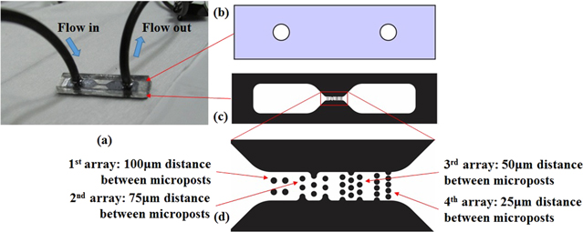
Figure 1. Image of completed filter microfluidic chip (a), design of top lid (b) and silicon substrate (c), four arrays of microposts with various distances between microposts from 25 μm to 100 μm (d).
Download figure:
Standard image High-resolution imageThe channel was designed with many arrays to avoid blocking by particles bigger than 25 μm. In fact, when solution with many various particle sizes flows through first array, particles bigger than 100 μm could be kept and let the particles smaller than 100 μm flow through. This function would be repeated for three remaining arrays. If microfluidic chip had only one array with 25 μm distance between microposts, all the particles bigger than 25 μm would be kept at this array, leading to the blockade of this chip. Moreover, all the corners of this chip have been rounded to make the particle move in and out easily, so that this chip can be washed back and re-worked many times.
2.3. Sample preparation
First of all, p-Si (100) wafer was initially cleaned following a standard procedure by using acetone, ethanol, piranha solution, HF and RCA cleaning solution. After that, silicon wafer was heated to 200 °C in 30 min Process of cleaning substrate is the important step to remove impurities on the surface of substrate and increases the adhesion of photoresist on the substrate.
HMDS was coated directly onto the silicon substrate by spin coating method. After coating HMDS, negative photoresist ma-N 1410 would be overlaid to the wafer by spin coating method with following parameters: speed of 500 rpm min−1 for 10 s and 3000 rpm min−1 for 30 s. Then the sample was heated to 100 °C for 90 s. These parameters are supplied by the manufacturer; thickness of photoresist was achieved about 1 μm.
The mask of microfluidic chip (figure 1(c)) was used for standard photolithography process. After that, a silver thin film was deposited by sputtering system Leybold Univex 350. Lift-off was then used to create hard mask of silver for DRIE process. Patterned silver on silicon sample after lift-off step was observed by optical microscope Olympus MX 51 (figure 2(a)). Process flow of entire fabrication process including photolithography, DRIE and bonding process is shown in figure 2(b).
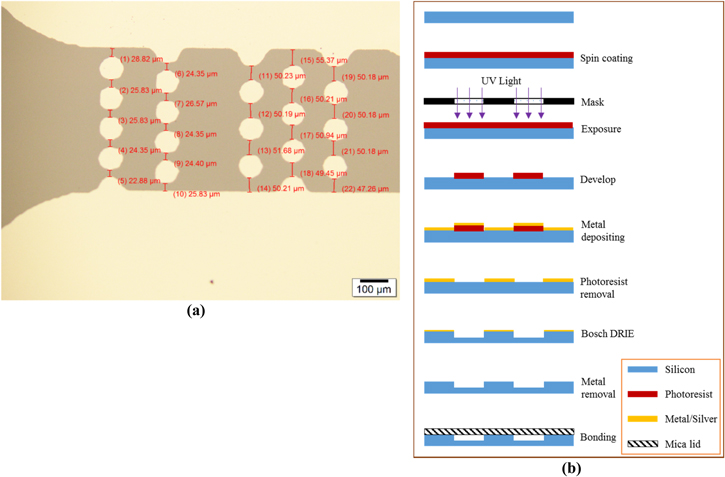
Figure 2. Patterned silver on silicon sample (a) and fabrication process flow for microfluidic chip (b).
Download figure:
Standard image High-resolution image2.4. Experiments of deep reactive ion etching (DRIE)
After lift-off step, a hard mask of silver was patterned on silicon substrate, then the sample would be anisotropically etched by DRIE system RIE 200-iPB from SAMCO, Japan. Requirements of etching step are vertical and smooth sidewall, obtained etched depth larger than 100 μm, overall good uniformity at the bottom surface of silicon channel. Based on reference [22], primary parameters of Bosch DRIE is shown in table 1. There exist some differences of parameters such as the pressure of cooling helium and the chamber pressure because of differences between DRIE systems which were used. The pressure of our chamber was controlled through the valve opening between the chamber and the vacuum pump. The percentage of valve opening was kept constant at 36%. Therefore, the chamber pressure is only influenced by the flow rate of the incoming gases. Moreover, between passivation and etching steps there is one second of delay time. These parameters were also similar with many Bosch DRIE recipes in following references [25, 28–30].
Table 1. Primary parameters of DRIE experiment [22].
| Process parameter | Passivation step | Etching step | Unit |
|---|---|---|---|
| C4F8 flow rate | 85 | 0.1 | sccm |
| SF6 flow rate | 0.1 | 130 | sccm |
| O2 flow rate | 0.1 | 13 | sccm |
| Percentage of valve opening | 36 | 36 | % |
| Inductive coupled plasma power | 600 | 600 | W |
| Bias power | 0 | 12 | W |
| He cooling | 2500 | 2500 | Pa |
| Duration | 8 | 12 | s |
| Number of cycles | 100 | 100 | cycle |
| Delay time | 1 | 1 | s |
The first experiment was performed using above primary parameters, but silicon could not be etched. It means that the flow rate of C4F8 was too high, leading to a thick passivation layer. It can be explained by the difference in DRIE equipments. Therefore, in this paper, the bias power, duration of a cycle and oxygen presence were investigated to obtain vertical and smooth sidewall, deep silicon features and good uniformity in bottom surface.
After DRIE, the silver hard mask was removed by using a piranha solution, a mixture comprising 3 parts of sulfuric acid and 1 part of hydrogen peroxide. Then, samples were soaked in HF 5% to achieve hydrophobic surface. Top view and cross-section view of the silicon samples were observed by optical microscope Olympus MX51 and SEM Jeol JSM-6480LV. The depth of the silicon features were measured by mechanical profilometry (DEKTAK 6 M).
2.5. Adhesive bonding
Two ports were created on mica top lid to connect with viton tube by laser cutting machine. After that, mica top lid and silicon substrate were bonded by using SU-8. A thin layer of SU-8 was dropped in mica top lid and silicon substrate. Viton tube was also connected with top mica lid by SU-8. After that, two parts were put together and heated to 120 °C in one hour.
2.6. Filter testing
Viton tube of microfluidic chip was connected with peristaltic pump FH 10 from Thermo Scientific to pump solution into microfluidic chip. Microfluidic chip was immobilized by using double clip. A mixture of clay and mud with various particle size was used for testing. Particle size of pre-filter solution and post-filter solution were measured by using optical microscope Olympus MX51 and SEM Jeol JSM-6480LV.
3. Results and discussion
3.1. The influences of bias power
The first experiment was performed by using the parameters in table 1, but no silicon trenches could be formed. It means that the flow rate of C4F8 was too high, leading to a thick passivation layer. The bias power at 12 W was too low to etch thick passivation layer. Therefore, in following experiments the bias power was increased from 12 W to 36 W, 48 W, 60 W and 72 W (table 2). The depth of silicon features after DRIE process is shown in table 2. The influence of bias power on the depth of silicon features is shown in figure 3. Top view image from optical microscopy and cross section image from SEM of four samples: MC-36W, MC-48W, MC-60W and MC-72W are shown in figure 4.
Table 2. Depth of silicon features for different bias power.
| Sample | Bias power (W) | Depth (μm) | Etch rate (μm min−1) | Etched depth per cycle (μm/cycle) |
|---|---|---|---|---|
| MC-12W | 12 | 0 | 0 | 0 |
| MC-36W | 36 | 80 | 2.402 | 0.8 |
| MC-48W | 48 | 167 | 5.015 | 1.67 |
| MC-60W | 60 | 176 | 5.285 | 1.76 |
| MC-72W | 72 | 166 | 4.985 | 1.66 |

Figure 3. Influence of bias power on the depth of silicon features.
Download figure:
Standard image High-resolution image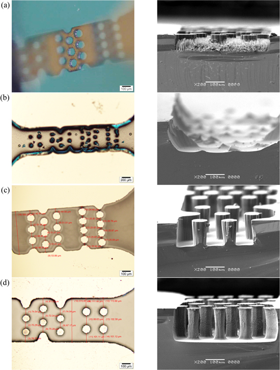
Figure 4. Top view images from optical microscopy (left) and cross section images from SEM (right) of four samples: (a) MC-36W, (b) MC-48W, (c) MC-60W and (d) MC-72W.
Download figure:
Standard image High-resolution imageGenerally, increasing bias power from 12 W to 48 W leads to a significant increase of depth of silicon features (figure 3). When bias power was increased from 48 W to 60 W or 72 W, the etched depth was not changed so much. Bias power would accelerate fluorine radicals and ions to bottom surface and increase the physical etching in Bosch DRIE process which is the combination of physical etching and chemical etching. Bias power at 48 W could be considered as high enough to accelerate radicals and ions to bottom surface, thus there was no much differences between etched depth at 48 W, 60 W and 72 W. With the goal of obtaining etched depth more than 100 μm, bias power at 48 W, 60 W and 72 W can be considered as suitable parameter.
However, etch profiles between four samples at different bias powers were significantly different. At bias power of 36 W, a lot of thin grasses were formed at the bottom surface (figure 4(a)). With bias power of 48 W, almost all microposts were etched away. While bias power was at 60 W, the microposts had a small slope, but the uniformity at the bottom surface and smoothness of sidewall could be accepted. Sidewall of microposts was rough when bias power increased to 72 W.
The goal of this work is to fabricate vertical, smooth sidewall with good uniformity at the bottom surface, thus 60 W of bias power was selected for next experiments. Microposts of sample MC-60W also had problem of small slope, but this problem could be overcome by adjusting some different parameters such as duration per cycle or oxygen presence in following experiments.
3.2. The influence of oxygen presence and duration per cycle
According to results in section 3.1, the bias power of 60 W was chosen for the next experiments. In [25], it was shown that many parameters of Bosch DRIE process can be adjusted to obtain vertical and smooth sidewall such as C4F8 flow rate, SF6, pressure, fluorine-to-carbon ratio or etch-to-deposition rate. In this work two different parameters namely duration per cycle and oxygen presence were studied. With primary parameters in table 1, duration of a cycle composed of passivation step and etching step was 20 s and the ratio of passivation duration to etching duration was 8/12. In next experiments, ratio of passivation duration to etching duration was kept invariable at 2/3, but duration per cycle was changed from 20 s to 15, 10 and 5 s. The number of cycles was also changed to keep total passivation and etching time for Bosch DRIE process invariable. Besides that, oxygen presence was also studied to explore the influence of oxygen to etch profile. There were 8 samples in following experiments which have been shown in table 3. Influence of duration per cycle and oxygen presence on etched depth and etched depth per cycle have been shown in figure 5 and SEM images of these 8 samples have been shown in figure 6.
Table 3. Etched depth for different duration per cycle and oxygen presence.
| Sample | Duration per cycle | Passivation/Etching time (s) | Number of cycles (cycles) | O2 flow rate (sccm) | Depth (μm) | Etched depth per cycle (μm/cycle) |
|---|---|---|---|---|---|---|
| MC-1 | 20 | 8/12 | 100 | 13 | 176 | 1.76 |
| MC-2 | 15 | 6/9 | 133 | 180 | 1.35 | |
| MC-3 | 10 | 4/6 | 200 | 184 | 0.92 | |
| MC-4 | 5 | 2/3 | 400 | 187 | 0.47 | |
| MC-5 | 20 | 8/12 | 100 | 0 | 173 | 1.73 |
| MC-6 | 15 | 6/9 | 133 | 166 | 1.25 | |
| MC-7 | 10 | 4/6 | 200 | 163 | 0.82 | |
| MC-8 | 5 | 2/3 | 400 | 150 | 0.38 | |
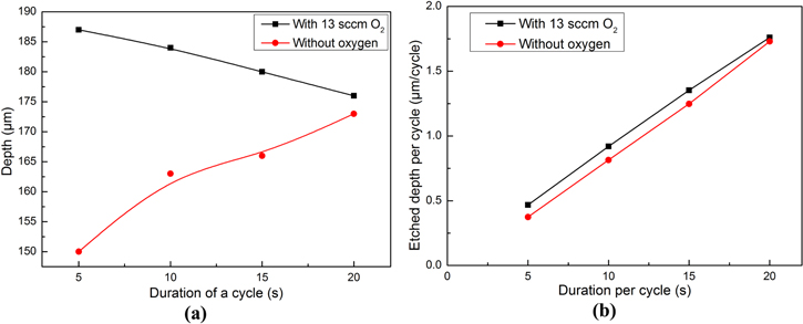
Figure 5. Influence of duration per cycle and oxygen presence on (a) the etched depth and (b) the etched depth per cycle.
Download figure:
Standard image High-resolution image
Figure 6. SEM images of eight samples: (a) MC-1, (b) MC-2, (c) MC-3, (d) MC-4, (e) MC-5, (f) MC-6, (g) MC-7 and (h) MC-8.
Download figure:
Standard image High-resolution imageIn general, the absence of oxygen in Bosch DRIE process led to the decrease of etched depth and etched depth per cycle (figure 5). This result could be explained as follows: O2 helped to create more F-atom because of the reaction between O2, O* and  SF6 [24]. Therefore, with oxygen presence, passivation layer was etched faster, leading to higher etch rate as well as damage of microposts. In fact, SEM image of four samples: MC-1, MC-2, MC-3 and MC-4 (figure 6) have shown that all microposts had been damaged in Bosch DRIE process with oxygen presence, especially almost microposts of MC-3 and MC-4 was etched away. Otherwise, SEM image of four samples: MC-5, MC-6, MC-7 and MC-8 in figure 6 showed better etch profile, almost microposts were not etched away. Therefore, these results could conclude that the oxygen presence would lead to higher passivation layer etch rate, higher etch rate and more difficulty to obtain vertical sidewall for Bosch DRIE process.
In figure 5(b), etched depth per cycle (Y) showed a linear dependence with duration per cycle (X). Linear regression was performed to understand linear dependence between etched depth per cycle and duration per cycle by software OriginPro 8.5.1


These results are shown in table 4. The coefficient of determination is good, near to a value of 1. Slope of equation (2) is larger than that of equation (3), leading to conclusion of higher etch rate when oxygen is present in Bosch DRIE process. This linear dependence was also suitable with three-stage model in reference [21]. In this model, etching step is divided into two steps of polymer removal and isotropic silicon etching, thus with the longer duration per cycle, time for passivation deposition, passivation removal and isotropic etch were also longer. Therefore, etched depth per cycle would increase linearly with duration per cycle.
Table 4. Linear regression equation between etched depth per cycle and duration per cycle.
| Equation | Condition | Coefficient of determination |
|---|---|---|
| (2) | with 13 sccm O2 | 0.9996 |
| (3) | without oxygen | 0.9987 |
Although etched depth per cycle showed a linear dependence with duration per cycle, etched depth and etch profile between sample with 100 cycles of 20 s and sample with 400 cycles of 5 s showed large differences (figures 5 and 6). Therefore it is necessary to study in detail the duration per cycle in order to understand the influence of this parameter on etching process. Moreover, there is another parameter: the switching time. Its effect on DRIE process must be also understood. In [27], switching time between etching step and passivation step had been considered as the key parameter to obtain smooth sidewall. The reason why fast switching time could help to obtain good etch profile had not been told in [27], but we thought fast switching time can be utilized to adjust etch-to-deposition ratio. In fact, after the deposition of passivation layer, etching step took place, subsequently deposition step would take place, again and again, leading to thin passivation layer and short duration of etching step. Combination with three-stage model in [21], when etching step was shorter, duration for isotropic etching step would be shorter, and thus sidewall could become smoother and more vertical. Based on this conclusion, duration per cycle can be considered as a key parameter to adjust etch-to-deposition ratio for Bosch DRIE process. When the duration per cycle decreased, etching step would become shorter and isotropic etching step would also become shorter.
Two series of experiments were performed to study in detail the influence of the oxygen presence to the etched depth. In the first series of experiments four samples MC-1, MC-2, MC-3 and MC-4 were dry etched by Bosch DRIE process with duration per cycle decreasing from 20 to 5 s in presence of oxygen. In this case the edched depth increases from 176 t0 187 μm. In the second series of experiments four samples MC-5, MC-6, MC-7 and MC-8 were dry etched by Bosch DRIE process with duration per cycle decreasing from 20 to 5 s without oxygen. In this case the edched depth decreases from 173 to 150 μm.
The difference can be explained by the presence of O2 in etching step. In Bosch DRIE process oxygen has two roles: creating higher F-atom density to etch passivation layer as well as silicon faster [24] and forming passivating layer of oxide-fluoride compound (SiOxFy) after removing passivation layer [24, 25]. First role of O2 showed the higher etch rate (figure 5) and the second role of O2 could be used to explained these results. In fact, when the duration per cycle decreased, duration for isotropic etching also decreased, so that thinner passivating layer of oxide-fluoride compound was formed. Therefore, when duration per cycle decreased, the etched depth also increased. The thinner passivating layer of oxide-fluoride compound also led to the removal of microposts (figures 6(c) and (d)).
SEM image of 8 samples in figure 6 showed that sidewall of sample MC-8 was vertical and smooth enough for microfluidic chip. The optimized parameters of Bosch DRIE were 60 W bias power, 2 s for passivation step, 3 s for etching step, 400 loops and without oxygen. These parameters would be used to fabricate complete filter microfluidic chip.
3.3. Filtration testing of microfluidic chip
Microfluidic chip was formed after adhesive bonding silicon substrate with mica lid and connecting with viton tube by SU-8 (figure 1(a)). Microfluidic chip was kept immobilized by double clip and was connected with peristaltic pump FH 10 from Thermo Scientific. A mixture of clay and mud was used for this test (figure 7(a)). Pre-filter and post-filter solutions are shown in figure 7(b), the post-filter solution was purifier. Particle size of pre-filter and post-filter solution was measured by SEM and optical microscopy (figure 8). It is obvious to see that there are many particles larger than 25 μm and smaller than 25 μm in pre-filter solution (figure 8(a)). After filtering, almost particles were smaller than 25 μm (figure 8(b)). Therefore, microfluidic chip works well in particle filtration testing.
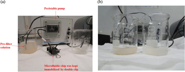
Figure 7. Testing microfluidic chip with (a) peristaltic pump, and (b) pre-filter and post-filter solution.
Download figure:
Standard image High-resolution image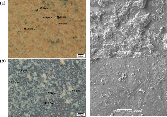
Figure 8. Optical microscopy images (left) and SEM images (right) of (a) pre-filter solution and (b) post-filter solution.
Download figure:
Standard image High-resolution image
4. Conclusion
In this paper the entire fabrication process of filter silicon microfluidic chip including photolithography, Bosch DRIE process and bonding has been presented. Many parameters such as bias power, duration of a cycle and oxygen presence were studied to obtain silicon features with good vertical sidewall and etched depth at 150 μm. The optimized parameters for Bosch DRIE process were 60 W bias power, 2 s for passivation step, 3 s for etching step, 400 loops and without oxygen. These parameters were applied to fabricate filter a silicon microfluidic chip with four arrays of microposts with various distances between microposts from 100 to 25 μm. Result of filtration testing showed that only particles smaller than 25 μm can go through thr filter microfluidic chip. This chip can be applied in many research fields such as inkjet printing technology, particle filtration, particle capturing etc.
Acknowledgments
The authors highly appreciate the financial support of the Vietnam National University in Ho Chi Minh City (VNU-HCM) under grant number HS2015-32-01.
Footnotes
- *
Invited talk at 8th International Workshop on Advanced Materials Science and Nanotechnology (IWAMSN2016), 8-12 November 2016, Ha Long City, Vietnam.