
Abstract
The quantitative assessment of the nanoscale gate stack double gate (GS-DG) MOSFET performance values are numerically calculated with different gate metal work functions (Φm = 4.52 eV, 4.6 eV, 4.7 eV). The effect of electrostatic control on dc, analog and RF figures of merit (FOMs) which includes subthreshold slope (SS), drain induced barrier lowering (DIBL), transconductance generation factor (TGF), early voltage (VEA), intrinsic gain (AV), cut off frequency (fT) and transconductance frequency product (TFP), gain frequency product (GFP) and gain transconductance frequency product (GTFP) have been investigated for the model GS-DG MOSFET. Higher TGF and AV was achieved with Φm = 4.6 eV for the device. For a better comparison among the analog/RF FOMs, the threshold voltage (Vth) is maintained at a constant value for different work function cases. To achieve a constant Vth, the channel doping (NA) and source/drain doping (ND) is tuned accordingly for all device cases. Superior fT which is due to higher transconductance (gm) and lower output conductance (gd), was observed for the device. In addition, better gain performances i.e. GFP and GTFP were achieved resulting from improved gm. Thus, the device structure modelled with Φm of 4.6 eV can be considered as a better candidate for analog and RF circuit applications.
Export citation and abstract BibTeX RIS

Original content from this work may be used under the terms of the Creative Commons Attribution 3.0 licence. Any further distribution of this work must maintain attribution to the author(s) and the title of the work, journal citation and DOI.
1. Introduction
The progress of semiconductor electronic devices has made a rapid improvement of performance and low cost application. The advancement in complexity of complementary metal-oxide-semiconductor (CMOS) design has been achieved by scaling geometric dimensions of the metal oxide semiconductor field-effect-transistor (MOSFET). The scaling of MOSFET in electronic circuits has led to an increase in the performance in electronic systems with more features and higher processing speed, while performance-to-cost ratio is also rising. This process has been successful for almost fifty years. Research is still going on to find devices that work in high frequencies, with low power consumption at nanometer dimension [1–4].
According to ITRS-2011 [5], a precisely controlled process flow for the incorporation of new technologies is becoming crucial for deep sub-micron devices. Among the possible solutions, unconventional metal-oxide-semiconductor (MOS) structures employing asymmetric structures have been proposed to overcome the short channel effects (SCEs). Also, double gate (DG) structures fabricated on silicon-on-insulator (SOI) wafers have been utilized in CMOS technology due to their excellent scaling capability, outstanding SCEs immunity, high current drivability (Ion) and transconductance (gm) and lower leakage current (Ioff) compared to the bulk MOSFETs [6–11]. Also, the body thickness is made much less, by which the centroid of the inversion charge moves from the interface to the middle. The electric field in the middle of the body combined with the volume inversion, which enhances the mobility.
Recently, the market demand has tremendously increased for ultralow power applications. MOSFETs operated in subthreshold region have created a lot of interest for such applications. MOSFETs in the subthreshold region of operation have an advantage of having significant high gain due to exponential behavior of the drain current which gives rise to higher transconductance generation factor (gm/ID) in the subthreshold regime [12–16]. Sharma et al [17] provide a detailed analysis about many analog/RF figures of merit (FOMs) for different type of structures on double gate platform. Quite a few reports [18] are available on the adjustment of metal work function for suitable applications. However, there are no such reports available to explore the impact of work function on analog and RF performances of GS-DG MOSFET.
In this paper extensive simulations have been carried out to study various important electrostatic and dynamic parameters of DG-MOSFET with high-k metal gate (HKMG) technology by varying the work function of the gate metal. To find out the proper metal for HKMG technology, the investigation is carried out for a variable metal work function by keeping in mind constant threshold voltage. Along with the introduction, section 2 describes the device description that includes all the dimensions, materials and doping concentrations of HKMG DG-MOSFET. Section 3 gives the physical principles of the device under study. It also describes the mutual dependence between the physical parameters presented in the simulation results. Section 4 analyses the physics of the device using device numerical simulations and models activated for simulation. Section 5 comprises the analog and RF performance matrices of the device. Including SCEs such as SS and DIBL, various important analog and RF figures of merit (FOMs) such as transconductance generation factor (TGF), early voltage (VEA), intrinsic gain (Av), cut off frequency (fT) and transconductance frequency product (TFP), gain frequency product (GFP) and gain transconductance frequency product (GTFP) have been closely observed by varying the gate metal work function for different configurations. Finally, the concluding remarks in section 6 substantiate the novelty of the paper.
2. Basic device dimension
A planar symmetric GS-DG MOSFET has been considered whose schematic structure is shown in figure 1. An ultrathin SOI MOSFET requires film thickness just one fourth of the channel length for better control of transistor electrostatics [6]. So the silicon film thickness (tSi) is considered as 10 nm. For a better comparison of analog/RF FOMs, the threshold voltage (Vth) is maintained at a constant value of 0.2 V while varying the work function at VDS = 0.1 V.
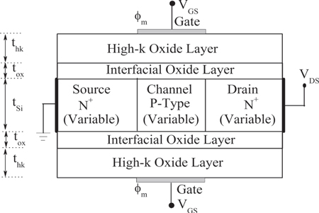
Figure 1. Schematic structure of GS-DG MOSFET.
Download figure:
Standard image High-resolution imageThe channel doping (NA) and source/drain doping (ND) are changed to maintain the constant Vth which is tabulated in table 1. Source and drain extensions are 60 nm long from the edges of the gates, with metal contacts vertically placed at their ends. The channel length of the device is fixed at 40 nm.
Table 1. Device parameters under study.
| Metal gate work function Φm or WF (eV) | Channel doping NA (cm−3) | Channel doping ND (cm−3) |
|---|---|---|
| 4.52 (Ag) | 1.5 × 10¹⁸ | 1.0 × 10²⁰ |
| 4.6 (Mo) | 1.0 × 10¹⁶ | 1.0 × 10²⁰ |
| 4.7 (Au) | 1.0 × 10¹⁵ | 9.0 × 10²¹ |
For the HKMG technology, the gate stack configuration has been considered with hafnium dioxide (HfO2) sandwiched over silicon dioxide (SiO2) layer. The interfacial layer (SiO2) thickness (tox) and above this high-k oxide layer (thk) are fixed at 0.6 nm, 0.5 nm (equivalent thickness of high-k), respectively, so to achieve equivalent oxide thickness (EOT) of 1.1 nm.
3. Physical principle of device
The threshold voltage (Vth) can be defined quantitatively as the gate voltage at which the minimum carrier charge density reaches certain value to achieve turn on condition. This definition is equivalent to the constant drain current (ID) method of Vth extraction, which is widely used in numerical simulation and experimental measurements [19].
The threshold voltage can be expressed as

where Φms is the work function difference between metal gate and semiconductor, ϕch is the potential in the channel. To achieve a constant threshold voltage with the variation of metal gate work function, the doping concentrations (NA, ND) are tuned, which change the built in potential (Vbi) of the device given as

In symmetric DG-MOSFET with Pao-Sah's gradual channel approximation, the generalized behaviour of the device for all regions of operation reported by Taur et al [20] is determined by the following equation

According to equation (3) with constant Vth, the current ID needs to be constant for all cases. However, the mobility decreases when the channel doping increases to maintain a constant Vth in case of lower metal gate work functions. Depending on the variation of current, the analog/RF performances are analysed in section 5.
4. Simulation procedure
The 2-D numerical device simulator [21], ATLAS is employed to simulate the n-channel planner DG-MOSFET with high-k metal gate. According to ITRS the drain bias has been fixed at VDD = 1.0 V [5]. To study the analog performance the simulation is carried out with drain to source voltage VDS = 0.5 V (which is half of the supply voltage i.e., VDD/2) [22] with a variable gate to source voltage VGS = 0 V to 1.0 V. Threshold voltage (Vth) is extracted using constant current (ID = 10−6 A μm−1) definition from the ID−VGS transfer characteristic at VDS = 0.1 V. The threshold voltage is used to find out the gate overdrive voltage (VGT = VGS − Vth). The gate overdrive voltage is an important property of amplifier circuit as it decides the region of operation. The increment of VGT increases drain current until saturation. Hence, in our investigation all the analog and RF analysis has been done against VGT [23, 24]. To enhance the accuracy in the results, for MOSFET simulation the inversion-layer Lombardi constant voltage and temperature mobility model has been used. The Shockley–Read–Hall generation and recombination parameters simulating the leakage currents that exist due to thermal generation are incorporated in the simulation. The model Fermi–Dirac uses a rational Chebyshev approximation that gives results close to the exact values. The Auger recombination models for minority carrier recombination have been activated. In this simulation all the junctions of the structure are assumed as abrupt and the biasing conditions are considered at room temperature. Furthermore, two numerical techniques Gummel and Newton have been chosen to obtain solutions [21].
5. Results and discussion
Figure 2(a) shows drain current (ID) in both linear and log scale as a function of gate to source voltage (VGS) for different gate work function at drain bias (VDS) of 0.5 V. The drain current is dependent on the mobility (μ) of carriers which is controlled by the doping concentrations. Here in the low work function metal gate device the channel doping (NA) is kept high which results a lower drain current (ID) then the device having higher NA, because the mobility is directly proportional to the current as shown in equation (3). We found that the drain current increases with the increase of work function.

Figure 2. (a) Drain current (ID) in both linear and log scale as a function of gate to source voltage (VGS). (b) Output conductance (gd) and drain current (ID) with respect to drain to source voltage (VDS) for different work functions.
Download figure:
Standard image High-resolution imageThe sub threshold slope (SS) is the major parameter for calculating the off state current. Furthermore, SS is calculated by the formula

The value of drain induced barrier lowering (DIBL) is calculated by using the relation:  . The DIBL calculation is performed for Vth at VDS = 0.1 V and VDS = 1.0 V. Both the extracted value of SS and calculated value of DIBL for different work functions are tabulated in table 2. From figure 2(a), the on current increases as work function of the device increases and reaches maximum at 4.7 eV. The off current is quite constant for all device cases as Vth is maintained constant. Output conductance (gd) and drain current (ID) with respect to drain to source voltage (VDS) for different work functions are plotted in figure 2(b). From the figure, output current is maximum for 4.6 eV device case and lowest for 4.7 eV device case.
Table 2. Electrostatic and analog performances for different values of work function, VD = 0.5 V.
| Work function (eV) | DIBL (mV V−1) | SS (mV decade−1) | Transconductance, gm (S) | Output conductance, gd (S) | Early voltage, VEA (V) | Gain, AV (dB) | TGF (V−1) |
|---|---|---|---|---|---|---|---|
| 4.52 | 20.43 | 62.58 | 2.56E − 03 | 3.45E − 05 | 9.71 | 37.42 | 39.395 |
| 4.6 | 19.96 | 62.06 | 3.04E − 03 | 2.12E − 05 | 17.81 | 43.12 | 41.173 |
| 4.7 | 21.48 | 63.23 | 3.28E − 03 | 2.11E − 05 | 8.46 | 43.81 | 41.186 |
As far as analog circuits are concerned, the most important parameters are the transconductance (gm), output conductance (gd), early voltage (VEA), transconductance-to-drain current ratio (gm/Id), intrinsic gain (gm/gd), terminal capacitances, i.e., gate-to-source capacitance (Cgs) and gate-to-drain capacitance (Cgd), and cutoff frequency (fT). The gm–VGT and TGF–VGT characteristics have been compared for various work functions in figure 3(a). In references [12, 15, 24] it was shown that


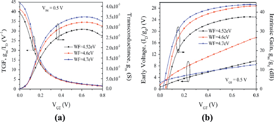
Figure 3. (a) Transconductance generation factor (TGF) and transconductance (gm) as a function of gate over drive voltage (VGT). (b) Early voltage (VEA) and intrinsic gain (AV) as a function of gate over drive voltage (VGT) for different work functions.
Download figure:
Standard image High-resolution imageThe gm/ID ratio demonstrates how efficiently the current is used to achieve a certain value of transconductance. The advantage of high transconductance-to-drain ratio is the realization of circuits operating at low supply voltage. From the analysis, the structure having work function of 4.7 eV shows high drain current. According to the above relation it is clear that both gm and TGF are directly dependent on the drain current. So, the structure having work function of 4.7 eV gives rise to higher values of transconductance and TGF when compared with others. Early voltage (VEA) and intrinsic gain (AV) as functions of gate over drive voltage (VGT) for different work functions are presented in figure 3(b). An improvement is observed in VEA for work function of 4.6 eV when compared to others. The intrinsic gain of the device, which is the ratio of transconductance and output conductance for various gate work functions is also displayed against gate over drive voltage (VGT) for VDS = 0.5 V in figure 3(b). The simulated results for subthreshold slope (SS), maximum value of transconductance and maximum value of output conductance are outlined in table 2. By comparing these values while work function varying from 4.52 eV to 4.6 eV, SS value is decreased by 0.83%, DIBL value is decreased 2.3% and gd is decreased by 62.73%. In analog/RF figures of merit transconductance (gm) is increased by 18.75%, transconductance-to-drain-current ratio gm/ID is improved by 4.51%, intrinsic gain gm/gd increases by 15.23%, and early voltage VEA is increased by 83.41% while coming from 4.52 eV to 4.6 eV device case. By comparing the device having 4.6 eV provides better values in case of VEA, gain and TGF as compared to 4.52 eV case and nearly equal values with 4.7 eV case.
Figure 4 shows the intrinsic capacitances (gate to source capacitance Cgs and gate to drain capacitance Cgd) as a function of VGT for both subthreshold or weak inversion and super threshold or strong inversion regions. As shown in figure, in the subthreshold regime, the intrinsic capacitance parameters have low values which increase slowly; however, in the super threshold region, they increase swiftly. This is because of the increase in the fringing field lines emanating from the gate edges. The device having work function 4.7 eV shows high value for Cgs and device having 4.52 eV gives high Cgd when compared to others. However, in the case of 4.6 eV, both the intrinsic capacitance values are least which in turn leads to high cutoff frequency.
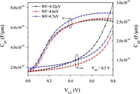
Figure 4. Gate to source capacitance (Cgs) and gate to drain capacitance (Cgd) as a function of gate over drive voltage (VGT) for different work functions.
Download figure:
Standard image High-resolution imageCutoff frequency fT is one of the most important parameters for evaluating the RF performance of the device. Generally, fT is the frequency when the current gain is unity:

From figure 5(a), the variations of cut off frequency (fT) and gain transconductance frequency product (GTFP) can be observed with respect to VGT for different values of work function. Here, the value of fT obtained for the device having high work function i.e. 4.7 eV is higher as compared to its counterparts. This is because, the gm value is high for work function of 4.7 eV and is low for the 4.52 eV case. To comprise these aspects of analog/RF circuit design, a unique figure of merit, GTFP  is analyzed. The variation of GTFP with gate over drive voltage (VGT) for different work functions is also shown in figure 5(a). It is interesting to see that as the gate work function increases, the GTFP also increases and it is highest for the device having work function of 4.7 eV. This is due to the reduction in peak electric field, lower output conductance of the device having work function of 4.7 eV.

Figure 5. (a) Cut off frequency (fT) and gain trans-conductance frequency product (GTFP). (b) Gain frequency product (GFP) and trans-conductance frequency product (TFP) as a function of gate over drive voltage (VGT) for different work functions.
Download figure:
Standard image High-resolution image
In figure 5(b) gives the gain frequency product  against gate overdrive voltage (VGT) for different values of work function. From the figure, the value of GFP increases as work function increases and reaches utmost for the device having work function of 4.7 eV. The product of gm/ID and fT represents a trade-off between power and bandwidth and is utilized in moderate to high speed designs. Transconductance frequency product (TFP) as a function of VGS for different values of work function is also plotted in figure 5(b). From the figure, it is clear that the device having higher work function gives higher TFP values than others. This is due to the high frequency values for higher work function devices.
These simulated results may be slightly higher than those of the experimental results, since, some considered parasitic parameters may be smaller than those of the real case, such as gate-to-source/drain capacitance, source/drain contact resistance. Cutoff frequency fT, transconductance frequency product  and gain transconductance frequency product
  are compared for various gate work functions.
All the extracted values for analog/RF FOMs are tabulated in table 3. Similarly, as work function increases from 4.52 eV to 4.6 eV, GFP of the device increases by 30.33%, cutoff frequency (fT) increases by 14.10%, TFP increases by 43.14% and GTFP is increased by 77.27%.
Table 3. RF performances for different values of work function.
| Work function (eV) | Cgs (fF) | Cgd (fF) | fT (GHz) | GFP (GHz) | TFP(GHz V−1) | GTFP (GHz V−1) |
|---|---|---|---|---|---|---|
| 4.52 | 0.673 | 0.297 | 547.262 | 1.98E + 04 | 5.98E + 03 | 1.32E + 05 |
| 4.6 | 0.690 | 0.222 | 624.471 | 2.58E + 04 | 8.56E + 03 | 2.34E + 05 |
| 4.7 | 0.745 | 0.240 | 674.428 | 2.87E + 04 | 9.98E + 03 | 3.08E + 05 |
6. Conclusion
A GS-DG MOSFET is explored in nanoscale regime by using device design guidelines. The impact of different gate metal work function (Φm ) on the device performance has been carried out in terms of dc, analog and RF application by keeping in mind a constant threshold voltage. Our calculated and simulated results show that the optimized value of gate work function will be 4.6 eV for the chosen device dimension. The selection of Φm was made with a trade-off between SS and DIBL in dc analysis. In connection with analog and RF application the device needs to be operated in sub-threshold regime and the performance values were optimized for gate metal work function 4.6 eV. When gate metal work function was raised from 4.52 eV to 4.6 eV, the SS and DIBL were decreased by 0.83% and 2.3%, respectively. Similarly, the output conductance (gd) is decreased by 62.73%, and AV is increased by 15.23% in 4.6 eV case. These results enhance the important FOMs of the technology, i.e. TGF by 4.51%, fT by 14.10%, TFP by 43.13%, GFP by 30.3% and GTFP by 77.27% for the 4.6 eV device case as compare to its counterpart the 4.52 eV case. The result also shows that all the discussed parameters are more sensitive to the gate metal work function of the device. Depending on the requirement of the application, the performance of nanoscale DG-MOSFET can be improved by tuning the other device parameters with the device design guideline.