
Abstract
We present a micro-electrooptical iris based on the electrochromic polymer poly(3,4-ethylenedioxythiophene). Two ring-shaped concentric polymer-segments embedded in a transparent electrochemical cell form the micro iris. The polymer layers change their absorption when an external voltage is applied. This iris device benefits from the absence of any mechanically moving part. This renders a very slim design possible, which is suited for small integrated camera systems. During operation the polymer maintains its absorbing state without power consumption. Its low driving voltage of maximum 1.5 V is beneficial for battery powered applications. The impact of the iris on the depth of focus and transmission control as well as its dynamical behavior will be addressed.
Export citation and abstract BibTeX RIS
1. Introduction
In the last decade, the global interest in high-tech consumer electronics with integrated cameras, e.g., smartphones, tablet computers, and notebooks has increased the demand for compact and advanced optical systems. One of the important components of a top grade camera is the iris aperture. In general it has two mayor functions: control of the light intensity to increase the maximum possible dynamic range of the image sensor and tuning the depth of focus (DoF) by cutting off marginal rays. Despite the desire to include these vital functions, there are still no iris apertures today available that meet all the challenging requirements set by small integrated systems.
The conventional macroscopic mechanical iris diaphragm used in cameras is made from a set of blades. They overlap to form an aperture of polygonal shape and are moved mechanically to adjust the aperture size. Miniaturization of these devices is limited because of at least two reasons: some kind of actuation is required to move the blades and they need sufficient space outside the optical path, when the iris is completely opened. In case of compact integrated cameras for e.g., smart phones this space requirement can not be satisfied. This problem has already been addressed by other groups offering several promising ideas. There are two major concepts to realize a micro-optical iris. Both rely on the motion of a strongly absorbing material into the path of light. The first approach is based on MEMS technology. Electrostatic actuators are used to deflect silicon blades [1–3] in such a way that an almost semi-circular aperture is formed. The second concept is based on a combination of an opaque and a transparent liquid that are immiscible. For transmission control several techniques were presented to move the opaque liquid to the desired area of the beam path. The most common approaches use pumps or electrostatic forces. But for now, the concepts are to space consuming to be implemented into small integrated systems. However, iris-designs based on electrowetting show promising properties but still require high voltages [4–6].
Electrochromic iris device differ from those designs because there is no motion of large amounts of absorbing material involved. Compared to the other concepts there is very limited work on them, but they have been considered for optical applications before [7–9]. The electrochromic iris consists of an electrochemical cell made of two sandwiched glass substrates each carrying a thin film electrochromic material on an underlying transparent electrode. The space between the electrodes is filled with an electrolyte. The latter provides the counter ions during the oxidation/reduction process of the EC material invoked by the application of an external voltage. The distinctive feature of electrochromic material is the dependence of the spectral absorbance from an externally applied electrochemical potential. The voltage range required to switch the aperture from the opaque to the transparent state is between  and
and  . Its worth to note that the actual electrochromic state can be maintained for hours without charge transfer. This leads to a very low power consumption suitable for battery powered applications. Exploiting these materials for an iris device reveals interesting properties for integrated systems, because of their low space- and energy requirement. The thickness of the current EC device including the active layer as well as the electrolyte is 55 μm, enabling a very slim design. The lateral space required outside the beam path comprises the area for the miniaturized electrical contact pads and sealing material.
2. Experimental details
2.1. Reagents
The monomer solution for the polymerization of poly(3,4- ethylenedioxythiophene) PEDOT is made from 0.02 M Edot (Aldrich) and 0.1 M LiCF SO
SO (Aldrich) in acetonitrile (99.99 % hplc grade). The electrolyte used in our devices is composed of 0.1 M LiCF
 SO
SO in propylene carbonate (99%, Aldrich). Glass slides (
 x
x  x
x  mm
mm ) covered with a conductive and optically transparent layer of indium tin oxide (ITO, thickness: 100 nm, resistivity: 8-12
  were purchased from Sigma-Aldrich. They were cleaned prior usage in a sequence of supersonic baths with acetone, isopropanol, and DI-water.
2.2. Design
Figure 1(a) illustrates the cross-section of our electrochromic device. Two sandwiched glass substrates are used as electrodes in the electrochemical cell, each carrying a transparent conductive ITO layer. Both electrodes additionally carry a 300 nm thin layer of the electrochromic polymer (PEDOT) [10]. As shown in figure 1(b) the polymer layers were structured into rings to establish the non-mechanical iris. The ITO layer was etched with an aqueous HCl solution to form the supporting electrode beneath the polymer as well as a thin film electrical conductor. The latter is required for the electrical contact with an external voltage supply. In the same process step, a second ITO electrode was defined on each substrate serving as counter electrode. Since this extra counter electrode is not covered with the EC-polymer, there should be no electrochemical reaction, thus the charge will be stored reversibly in the double layer.

Figure 1. (a) Cross section and (b) exploded view of the electrochromic iris.
Download figure:
Standard image High-resolution image2.3. Fabrication
In the first step a lift-off process was used to produce electrodes and alignment marks on each substrate consisting of a stack of 10 nm Cr and 90 nm Au. After that, PEDOT was electropolymerized from an EDOT monomer solution according to our recipe in [11]. The polymer layer and the underlying ITO layer were structured in another sequence of UV-lithography and wet and dry etching to form a single ring. The radii were adapted in such a way that the inner radius of the larger ring on one substrate slightly overlaps with the larger radius of the smaller ring of the other substrate if the rings are coaxially aligned. In this way we guarantee that there is no open annular area left between the two rings as was the case in a former iris device [11]. Then the substrates were bonded together in a bond aligner, forming the electrochemical cell. We used an UV-sensitive polymer-foil-resist (Ordyl SY 300, thickness: 55 μm) both as spacer and adhesive material. The foil is insulating and chemically stable after processing. UV-lithography and wet etching were used to define both the cell compartment and the necessary filling-channel. The electrolyte is loaded under vacuum conditions to minimize the enclosure of undesired ambient air inside the compartment. The filling channel is sealed with a vacuum tight epoxy resin (Torr Seal, Varian). More details on parameters and recipes were reported previously [11].
The finished device with the four possible switching states is shown in figure 2. Each of the two segments can be controlled individually. It is worth to note that the desired transmission of each segment can be precisely tuned by the amount of the applied external voltage enabling apodization of a light beam. In particular, the upper right picture shows the capability of our device to block specifically the inner ring of the beam. This is a prerequisite to use the EC iris for new applications like optical band pass Fourier filtering. This is an unique feature of individually switchable EC rings and impossible with a classic iris device. Finally, the device is framed with a metal holder (not shown in the images) to block scattered light as well as to facilitate its mechanical handling and mounting.

Figure 2. Images of the EC-iris in the four individual states. The upper right picture shows the special configuration where only the inner ring is opaque, while the outer ring is transparent.
Download figure:
Standard image High-resolution image3. Results and discussion
3.1. Intensity control
The basic application for the iris device is the control of light transmission. We measured the performance of the EC iris in the following way. The light from a cold light source (Schott KL 1500) was collimated with a lens and directed through the iris. The transmitted light was collected by a second lens, fed into an Ulbricht sphere, and measured with a spectrometer (Mikropack, plascalc 2000). The spectrum of the light passing through one iris segment is shown in figure 3(a) in the transparent and opaque state. For the measurement of transmitted light through the entire iris, the spectrometer was sensitive in the wavelength regime from 450 nm to 750 nm and the integral light intensity was measured. The EC segments of the iris were switched into the opaque state with a voltage of 1.5 V. To ensure that all segments are fully colored, the voltage was applied for two minutes. The results are shown in figure 3(b). The values are normalized and represent mean values of the measurements. The intensity was detected after consecutively switching the individual segments. Measurements revealed that the absorbed light was linearly dependent on the absorbing area of the segments. The maximum value of about 55% was observed when both rings are opaque.
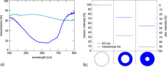
Figure 3. (a) Transmission spectra of one segment in transparent  and opaque
  state. (b) Transmitted light intensity of the EC iris for the three individual switching states. Scattering was assumed to be negligible.
Download figure:
Standard image High-resolution image3.2. Depth of Focus
For the investigation of the DoF three transparencies with laser printed text were placed at different distances to an imaging lens. The optical setup is shown in the bottom of figure 4. The distances of the transparencies were varied in such a way that one transparency was exactly in the image plane of the lens while the other two were installed in front of it and behind it, respectively. The transparencies were illuminated with a collimated beam through a color filter with 633 nm and their image was collected simultaneously with the image sensor of a commercial camera (Canon 450D) while placing the EC-iris or blade iris close to the lens. The gathered images for the EC iris and the blade iris are compiled in figure 4. With an open iris, the DoF is low, and thus only the text on the transparency in the image plane appears sharp, while the off-focus images are blurred. On closing the iris, the DoF is expected to continuously rise and thus the top and bottom text should appear more sharply. This behavior was proven for the blade iris in accordance with the theory. The EC iris behaves quite different owing to the limited absorption. Irrespective if the EC iris is completely switched on or off, the DoF is merely identical because it changes only the overall transmission. In fact, the experiment reveals that if only the outer ring is switched in the opaque state, the DoF increases (figure 4(b)) while it is reduced switching also the inner ring into the opaque state (figure 4(c)). Thus the DoF reaches a maximum for a medium aperture diameter that depends on the absorption. For a serious application of the EC iris, it is mandatory to have EC materials with improved absorption contrast available. In fact, the development of these materials is under lively development [12–14].
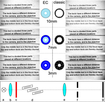
Figure 4. Images of three transparencies with consecutively raising image distance obtained for the three different states of the EC iris (left) and blade iris (right). Experimental setup (bottom): (a) light source, (b) collimation of light, (c) color filter @633 nm, (d) transparencies with 5 mm distance each, (e) lens (f = 150 mm), (f) EC-iris or blade iris, (g) image sensor.
Download figure:
Standard image High-resolution image3.3. Switching time
The transient response of the EC iris is an important feature for forthcoming applications. It is essentially determined by the electrical response of all impedances involved and the transport properties of charge carriers in the electrolyte and polymer film. It was optically investigated directing the beam of a HeNe laser (1 mW @ 632.8 nm) onto one side of the inner iris EC segment and measuring its transmission, while the electrodes were subject to a potential of 1.5 V in several configurations. From these experiments the switching time was deduced as the time necessary to rise the transmission from 10% to 90% (and vice versa).
When both the working and counter electrode are coated with a PEDOT layer—in our case the inner rings of the electrochemical cell—switching is rather fast owing to the similar reactivity of the two polymer films (figure 5(a)). The switching time for bleaching was 2 s, while coloring takes about 10 s. However, if ITO is used as counter electrode, the response time increases. This was verified (figure 5(b)) imposing the same potential to the PEDOT coated inner ring against the uncoated ITO electrode outside the optical path (see figure 1). In this configuration, bleaching takes up to 10 s and the colorization lasts almost 15 s. This behavior may indicate that the double layer forming on the ITO electrode is not sufficient enough to completely balance the charge, and emphasizes the importance of an electrochemically active counter electrode. Additionally, in each configuration bleaching is faster than the colorization process. This results presumably from the fact, that the conductivity of the PEDOT film is several orders of magnitude higher in the bleached state [15].
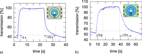
Figure 5. Transmission of the inner segment of the iris over time: (a) with PEDOT coated working and counter electrode and (b) with PEDOT coated working and bare ITO counter electrode.
Download figure:
Standard image High-resolution image3.4. Power consumption
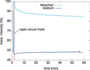
The capability of an EC material to maintain its redox state for a given electrochemical potential is referred to as memory effect. This ideal behavior is beneficial in particular for optical applications because it means that also the optical transmission state stays unaltered without additional charge transfer i.e., power consumption. In fact, experiments showed only a slight deviation from this ideal behavior. To study this in detail, we measured the intensity of the transmitted light after switching the state of the device. In each measurement the electrochemical potential was applied for 60 s to ensure that the polymer was completely switched into the proper redox state. Then the power supply was detached and the transmission was transiently measured for about one hour. The results are shown in figure 6.
Figure 6. Transient transmission of a 300 nm thin PEDOT layer after switching its redox state and detaching it from the power supply.
Download figure:
Standard image High-resolution image
The two states behaved slightly different. The opaque state of the electrochemically reduced polymer film shows very little change; the transmission increased by about 3% after one hour. The transparent state of the oxidized polymer is more prone to variations. After an initial 10% drop the transmission decreased by another 5% after one hour. This degradation of the oxidized state is presumably caused by unwanted redox reactions in the polymer matrix accompanied by the diffusion of the counter ions from the polymer into the electrolyte. Irrespective of the exact degradation process, after one hour the contrast has dropped from 55% to 37%. It therefore depends on the desired optical contrast in the application when the oxidized polymer state needs to be refreshed. The average power consumption for the refresh process can be roughly estimated. Switching of a segment takes less than 10 s and requires a current of about 20 μA at a voltage of 1.5 V. Due to the memory effect, refreshing needs to be repeated only once every hour. That leads to a power consumption of approximately 30 μW. Therefore, a conventional battery with a capacity of 1,200 mAh is sufficient to keep the iris-state for about 60,000 h.
4. Conclusion
We have presented a micro-iris designed for the application in small integrated optical system based on an electrochromic polymer film and studied its properties. The results proof that the EC iris can be utilized in principle to control the transmitted light and the DoF. However, the potential of the iris in its current state is mostly restricted by the insufficient absorption contrast and relatively long switching time of the commercially available PEDOT material. However, the synthesis of optimized EC materials is under rapid development. The exiguous power consumption of 30 μW per switching cycle at voltages as low as 1.5 V and the very low space requirements, make EC devices the ideal components for battery powered mobile applications.
Acknowledgements
We thank the German Research Foundation (DFG) for their financial support through Priority Program 1337 'Active Micro-optics'. We also thank the Nano Structuring Center (NSC) for their technical support and Carsten Kortz for his assistance with the measurements.