
Abstract
Undoped graphene is known to absorb 2.3% of visible light at a normal angle of incidence. In this paper, we theoretically demonstrate that the absorption of 10–100 GHz of an electromagnetic wave can be tuned from nearly 0 to 100% by varying the Fermi energy of graphene when the angle of incidence of the electromagnetic wave is kept within total internal reflection geometry. We calculate the absorption probability of the electromagnetic wave as a function of the Fermi energy of graphene and the angle of incidence of the wave. These results open up possibilities for the development of simple electromagnetic wave-switching devices operated by gate voltage.
Export citation and abstract BibTeX RIS
Graphene is a two-dimensional atomic layer of graphite that has various potential applications because of its unique electronic and optical properties. The linear energy dispersion relation of graphene results in effectively massless Dirac electrons and high carrier mobility.1–3) The high mobility of graphene has allowed researchers to develop ultrafast optoelectronic devices, such as field effect transistors and photodetectors, from the visible down to the near-infrared regimes.1,4)
It is well-known that undoped monolayer graphene absorbs 2.3% of visible light perpendicular to its surface, making graphene an almost perfect transparent conductor.2) Transparent graphene is useful for optical devices, such as liquid-crystal displays (LCDs) and light-emitting diodes (LEDs). However, in order to develop other optical devices, such as photodetectors, optical antennas, and solar cells, high optical absorption in graphene is required to generate a sufficiently large photocurrent. In recent years, the enhancement of the optical absorption of graphene has been extensively studied, but most research on the issue has involved the use of complicated techniques, such as using a grating coupler, or shaping the graphene into ribbons or disks.5–7) Practical optoelectronic applications of graphene thus remain challenging.
In this letter, we propose an alternative method to enhance the optical absorption of graphene for a microwave regime by simply varying the Fermi energy and the angle of incidence of an electromagnetic (EM) wave. The monolayer graphene is placed between two dielectric media to form a total internal reflection (TIR) geometry. Not only does this geometry allow us to enhance the EM wave absorption of monolayer graphene to up to 100%, it also allows us to suppress the absorption to nearly 0% by changing the Fermi energy of graphene.
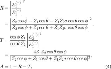
Our geometrical setup is shown schematically in Fig. 1. Graphene is modeled as a conducting interface between two dielectric media with dielectric constants ε1 and ε2. Unless otherwise defined, we assume that ε1 > ε2, which allows TIR to occur for the incident EM wave in medium 1. The absorption probability for this geometry can be calculated by utilizing the boundary conditions from Maxwell's equations. If we adopt the p-polarization of the EM wave, as shown in Fig. 1, we can obtain two boundary conditions for electric field E(i) and magnetic field H(i) ( ) as follows:


where the + (−) index denotes the right- (left-) going waves according to Fig. 1, θ is the angle of incidence and reflection, ϕ is the angle of refraction, and σ is the optical conductivity of graphene.8) The E and H fields are also related to each other in terms of the EM wave impedance in units of Ω for each medium:
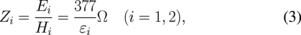
where the constant 377 Ω is the impedance of vacuum  . The quantities ϕ, θ, and Zi are related by Snell's law
  . Solving Eqs. (1)–(3), we obtain the reflectance R, the transmittance T, and the absorption probability A of the EM wave as follows:
where the values of R, T, and A can be denoted in terms of percentage (0–100%). Note that the factor Z1/Z2 in T of Eq. (4) is due to the different velocities of the EM wave in medium 1 and medium 2.
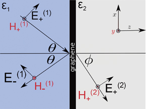
Fig. 1. Possible schematics to tune optical absorption in graphene. Graphene is placed between two dielectric media with dielectric constants ε1 and ε2. Graphene thickness is exaggerated. The incident EM wave forms an angle θ with the surface of medium 1 (left), and is refracted at angle ϕ into medium 2 (right). The EM wave is p-polarized.
Download figure:
Standard image High-resolution imageThe EM wave absorption A is determined by the optical conductivity σ, which describes the electron transition due to the optical absorption. Here, the σ for graphene is derived from the dielectric function ε using a random-phase approximation (RPA).9–11) Since the coupling between the EM wave and graphene occurs only at longer wavelengths, we focus our calculation only on the  case. At
  , the RPA dielectric function of graphene as a function of the wave vector q and the angular frequency ω of the EM wave for a given Fermi energy EF is expressed by10)
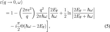
where e is the fundamental electron charge and Θ is the Heaviside step function. The relation between σ and ε is given by

and is obtained in  space.12) Using Eq. (6), σ can be written as
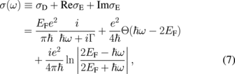
in which the q-dependence of σ has now vanished. The first term in Eq. (7) is the intraband conductivity, which is known as the Drude conductivity σD. We add spectral width Γ as a phenomenological parameter for the scattering rate. It depends on EF, as  ,13) where
  m/s is the Fermi velocity of graphene and μ = 104 cm2 V−1 s−1 is its electron mobility. The second and the third terms in Eq. (7) correspond to the real and imaginary parts, respectively, of interband conductivity σE. By inserting Eqs. (7) and (3) into Eq. (4), we get A, R, T as a function of EF and incidence angle θ. Both σD and σE affect EM wave absorption, and the contribution of each is discussed below.
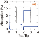
Let us see how EM wave absorption in graphene can be modified under certain conditions. In Fig. 2(a), we reproduce the 2.3% optical absorption if graphene is placed in a vacuum,2) i.e., ε1 = ε2 = 1 with EF = 0.64 eV and θ = 0°. The absorption A is associated with the real part of σ, as shown by the identical shape of both curves in Figs. 2(a) and 2(b).12) In Fig. 2(b), the conductivity of graphene [Eq. (7)] normalized by  is shown. The A value of 2.3% is obtained when
  [inset of Fig. 2(a)] because at this region, the real part of total conductivity σ is a constant σ0 [see Fig. 2(b)], which is obtained from
  (while σD is negligible). When
  [Fig. 2(a)], it can be seen that the A value becomes large (∼20%) due to Drude conductivity
  , as shown in Fig. 2(b). In this case,
  plays the major role in σ. Because of the large value of A in this region, we let the parameter
  meV (equivalent to f = 23.8 GHz, or microwave) and EF = 0.64 eV such that a large value of A is expected when the incident angle θ is changed.
Download figure:
Standard image High-resolution image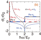
Fig. 2. (a) The absorption spectra of EM wave at EF = 0.64 eV, ε1 = ε2 = 1, and θ = 0°. Inset shows the expanded section of absorption for  . (b) The normalized optical conductivity.
Download figure:
Standard image High-resolution imageIf ε1 > ε2, the TIR of the EM wave can occur at  , where θc is the critical angle defined by
  . When TIR occurs, no EM wave can be transmitted, and thus the EM wave can either be reflected or absorbed by graphene. Here, we set ε1 = 2.25 and ε2 = 1.25, which corresponds with θc = 48.19°. In Fig. 3(a), we show A, R, and T as functions of θ. As seen in Fig. 3(a), T = 0 if θ ≥ θc. Interestingly, A becomes almost unity at an angle of approximately 85°; hence, graphene absorbs all incoming EM waves, where R = 0. The dip in the A spectrum indicates the beginning of TIR, where R reaches its maximum value. In Fig. 3(b), we show the EF-dependence of A as a function of θ for several EF values. Furthermore, from each absorption peak obtained in Fig. 3(b), we can plot the maximum value of A and the corresponding peak position θmax as a function of EF [see Fig. 3(c)]. The maximum A value rapidly increases with increasing EF, and is saturated near 100% for EF ≥ 0.4 eV. For
  eV, A is nearly 0, as we can see in Fig. 3(b) and the inset of Fig. 3(c).
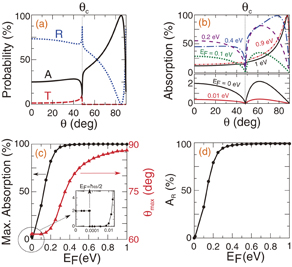
Fig. 3. (a) Absorption probability (A), reflectance (R), and transmittance (T). The A value of 0 (100%) expresses the zero (perfect) absorption of the EM wave. The graphene (EF = 0.64 eV) is sandwiched between two media with ε1 = 2.25 and ε2 = 1.25. (b) Absorption for several different EF values. (c) Maximum value of A as a function of EF and its corresponding position θmax, represented by circles and triangles, respectively. Inset shows the enlarged region of the maximum A for small EF values. (d) Absorption range (AR) as a function of EF.
Download figure:
Standard image High-resolution imageIt is expected that when EF decreases, A will monotonically decrease to zero. However, this is not the case, as we can see in Fig. 3(b) and the inset of Fig. 3(c). Even when we set EF to zero (or  ), the A value is approximately 2.2%. This is due to the vanishing intraband transition while interband transition dominates with total conductivity σ governed by constant σ0 for
  . Therefore, although EF decreases to zero, absorption is not zero. At the same time, for
  , Drude conductivity dominates, and conductivity is proportional to EF, as we can realize from Eq. (7). This is why the value of A for EF = 0.01 eV is smaller than that for EF = 0 eV. The θmax value shifts to the lower angle as the Fermi energy decreases, as shown in Fig. 3(c). This angle becomes a constant θmax = 61.16° at EF ≤ 0.1 eV. In Fig. 3(d), we define the absorption range (AR) as the difference between the A value at EF ≠ 0 and EF = 0 while keeping θmax for EF ≠ 0. We can see that AR starts to stabilize from EF = 0.4 eV at approximately 99%. This means that if we change EF from EF > 0.4 eV to zero, nearly perfect switching of the reflected EM wave can be observed, and this behavior can be useful for some applications.
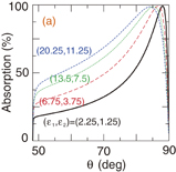
The dielectric constant of the surrounding medium can also affect the absorption of graphene, as shown in Fig. 4. In this case, we use  meV and EF = 1 eV. In Fig. 4(a), the ratio n of the dielectric constant of both media is kept constant, i.e., ε1/ε2 = n = 2.25/1.25 = 1.8, and we change both values of
  giving a constant θc = 48.19° where the plot starts. The absorption peak for all pairs of
  yields A values of almost 100%. The peak monotonically decreases from 88 to 84°, with increasing value of ε1 up to 20.25. When both ε1 and ε2 increase while keeping constant ε1/ε2 = n = 2.25/1.25 = 1.8, the peak moves to the smaller angle. The A spectrum as a function of θ becomes broader with increasing
  . In Fig. 4(b), we show the case where n is varied but ε2 = 1.25 is kept constant, i.e., ε1 = n × ε2. As the value of n increases, the maximum value of A stays almost 100%, but θmax is altered. The change in θmax is not pronounced if n < 100. In both Figs. 4(a) and 4(b), the maximum value of A does not change, even though we tune the surrounding dielectric constant. Hence, tuning the surrounding dielectric constant simply changes θmax. Figure 4(c) shows the dielectric constant-dependence of θmax. The relation between θmax and n can be expressed to contain a sinusoidal function. In Fig. 4(c),
  is plotted as a function of n for ε2 = 1.25 and ε2 = 3. It can be seen that
  depends linearly on n. The slope of the line depends on ε2, and becomes steeper when ε2 is large.
Download figure:
Standard image High-resolution image
Download figure:
Standard image High-resolution image
Fig. 4. (a) A for different dielectric constants of medium 1 and medium 2, where the ratio is kept constant. The depicted angle starts from θc = 48.19°. (b) A for different n, the ratio of the dielectric constant of medium 1 to that of medium 2. ε1 = n × ε2 and ε2 = 1.25. EF = 1 eV and  meV. (c) A peak position θmax as a function of n.
Download figure:
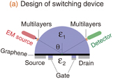
Standard image High-resolution imageTo apply all the concepts discussed so far, we show in Fig. 5(a) a possible design for an EM wave-switching device consisting of an EM wave source, a detector, a gate–voltage modulation system, and a graphene layer sandwiched between two dielectric materials  . The EM wave source is placed at a certain angle where absorption is maximum when EF ≠ 0. The detector is used to catch the reflected wave. It is necessary to insert thin, multi-layered films attached to medium 1 in front of the EM wave source and the detector in order to suppress unnecessary reflection at the surface of medium 1. The gates in the device are used to change the EF of the monolayer graphene. We may use electrochemical doping if medium 1 is an electrolyte. The top and bottom dielectric materials
  can be tuned to obtain large values of AR for perfect switching. In Fig. 5(b), for example, we used silicon as medium 1 (ε1 = 11.67 within the microwave frequency range) and vacuum as medium 2 (ε2 = 1). To obtain the EM wave switch, the EM wave with
  meV was shot at an incident angle of approximately θ = 62°. If the Fermi energy is changed from EF = 0.4 to 0 eV, we can detect the reflected EM wave with a reflectance of 0% to be nearly 100%, which corresponds with absorption from 100% to be nearly 0%, respectively.
Download figure:
Standard image High-resolution image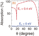
Fig. 5. (a) Possible design of an EM wave-switching device. Multi-layered films near the EM wave source and detector are intended to avoid unnecessary reflection. (b) Calculated absorption spectra as a function of the Fermi energy using ε1 = 11.67 (Si), ε2 = 1 (vacuum), and EM wave energy  meV (frequency of 23.8 GHz). It is possible to switch the EM wave at θ = 62° by changing EF = 0.4 to 0 eV.
Download figure:
Standard image High-resolution image
In conclusion, we have shown that the absorption of 10–100 GHz electromagnetic waves in graphene can be tuned from nearly 0 to 100% by simply varying the Fermi energy of graphene while keeping the EM wave within TIR geometry. We also designed a possible EM wave-switching device (with  meV, or a frequency of approximately 23.8 GHz) where switching behavior can be obtained by changing EF in the vicinity of 0–0.4 eV. Because of the simplicity of the device structure and its analytical formulation, we expect that experimental verification will be possible in the near future, which will allow us to determine how quickly the device can switch EM waves. We hope that our work also triggers further research on Fermi energy-dependence of EM wave absorption in graphene for frequency ranges beyond the 10–100 GHz regime.
Acknowledgments
M.S.U. and E.H. acknowledge the support of a MEXT scholarship. A.R.T.N. acknowledges the support of the Interdepartmental Doctoral Degree Program of Tohoku University, and R.S. acknowledges MEXT Grants Nos. 25286005 and 25107005. We are all grateful to Professor J. Kono (Rice University) for fruitful discussions which stimulated this work.