
Abstract
Nearly lattice-matched InAlN/AlxGa1−xN (x = 0.1, 0.21, and 0.34) heterostructures with a 1-nm-thick AlN interfacial layer were grown on AlN/sapphire templates by metalorganic chemical vapor deposition. Capacitance–voltage and Hall effect measurements revealed that two-dimensional electron gases (2DEGs) with high densities exceeding 2 × 10¹³/cm2 were generated at the heterointerface for all samples. It was confirmed that the generation of high-density 2DEGs can be explained as being due to internal polarization effects. The sheet resistance increased from 1,267 to 1,919 Ω/sq with the increase in Al content in the AlGaN channel, owing to the decreases in 2DEG density and mobility.
Export citation and abstract BibTeX RIS
High-electron-mobility transistors (HEMTs) based on AlGaN/GaN two-dimensional electron gas (2DEG) heterostructures are viewed as highly promising devices for high-power and/or high-frequency applications because of their excellent device features.1–4) In addition to conventional AlGaN/GaN heterostructures, advanced 2DEG heterostructures employing AlGaN channel layers5–17) or InAlN barrier layers18–25) have recently been examined with the aim of improving their electrical properties. In particular, since Nanjo et al. demonstrated ternary AlGaN-channel HEMTs with extremely high blocking capabilities,7) studies on these devices have been frequently reported.8–17) For example, Hatano and coworkers reported that AlGaN-channel HEMTs on AlN substrates showed a lower temperature dependence in DC and RF operations than conventional GaN-channel HEMTs.14,17) On the other hand, 2DEG heterostructures employing InAlN barrier layers instead of AlGaN barrier layers have also been attracting considerable attention. This is because lattice-matched InAlN/GaN heterostructures can yield a high 2DEG density of over 2.5 × 10¹³/cm2, without the generation of a high lattice strain, as a result of their large spontaneous polarization charges.18–20) This feature seems to be appropriate for high-drain-current operations. In fact, high 2DEG densities and excellent device performance have already been reported by some research groups.21–25) On the basis of the above findings, it seems natural to consider lattice-matched InAlN/AlGaN 2DEG heterostructures as candidates for future high-power electronic devices. However, no reports on InAlN/AlGaN 2DEG heterostructures have been published to date. Although Hiroki et al. have reported an InAlN/AlGaN/GaN heterostructure, its AlGaN layer was employed as a part of the barrier layer, not as a channel layer.26) In relation to InAlN/AlGaN heterostructures, we have reported the metalorganic chemical vapor deposition (MOCVD) of Al-rich AlGaN systems27) and lattice-matched InAlN/GaN heterostructures.20) In this study, we have attempted to grow lattice-matched InAlN/AlGaN heterostructures by MOCVD so as to examine their characteristics and potential. In addition to the MOCVD growth and structural and electrical characterizations, the measured 2DEG densities of the InAlN/AlGaN heterostructures have been discussed by considering their internal polarization effects.
Samples were grown in a horizontal MOCVD system (Taiyo Nippon Sanso SR2000), where trimethyl gallium, trimethyl aluminum, and trimethyl indium were used as group-III sources, and NH3 was used as a group-V source. A 2-in.-diameter AlN/sapphire template (DOWA Electronics) was used as an underlying substrate, which had a 1-µm-thick epitaxial AlN film on a c-face sapphire. The typical X-ray rocking curve (XRC) full widths at half maximum (FWHMs) of the epitaxial AlN film were approximately 100 and 1,500 s for the (0002) and  reflections, respectively. The InAlN/AlGaN heterostructures were grown to form, from bottom to top, a 2-µm-thick AlGaN channel layer, a 1-nm-thick AlN interfacial layer, and a 10-nm-thick InAlN barrier layer. The AlxGa1−xN (x = 0.1, 0.21, and 0.34) channel layers were grown directly on the AlN template without the use of any buffer layer technique. The 1-nm-thick AlN interfacial layer was employed not only for enhancing 2DEG carrier confinement in the channel but also for protecting the AlGaN surface during the growth interval.20,28) The InAlN barrier layers were grown to be lattice-matched to the underlying AlGaN channel layers, as will be described later. The layer thicknesses were estimated from the growth rate, and the compositions of the heterostructure samples were confirmed using X-ray diffraction (XRD) measurements. The depth profiling of the 2DEGs was evaluated using a capacitance–voltage (C–V) measurement system (Nanometrics ECVpro™), while the 2DEG densities and mobilities were determined by Hall effect measurement.
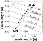
First, this study began with the characterization of the AlGaN layers for the 2DEG channel. Figure 1(a) shows the relationship between the a- and c-axis lengths of the AlGaN layers with varying Al content grown on the AlN templates. Here, the lattice strain and composition of the AlGaN layers were determined as29)

where C13 and C33 are the elastic stiffness constants, a0 and c0 are the room-temperature lattice constants of free-standing crystals, and a and c are the lattice constants of actual crystals, which were obtained by XRD measurements. In this equation, (a − a0)/a0 and (c − c0)/c0 represent the lattice strains εxx and εzz, respectively. The elastic and lattice constants of binary III–nitrides are listed in Table I.30,31) As for ternary AlGaN alloys, a0 and c0 were determined according to Vegard's law,32,33) and C13 and C33 were derived by linear interpolation.29) Consequently, perfectly relaxed AlGaN layers are plotted on the straight line between GaN and AlN in Fig. 1(a). In comparison along iso-composition lines (dashed lines) in this figure, the a-axis lengths in the actual AlGaN layers were obviously smaller than those indicated by the linear fit. It was thus confirmed that the AlGaN layers grown on the AlN template were strained in the direction of the in-plane compression. This tendency is almost consistent with previously reported results.27) As a result, the in-plane strain εxx in the AlGaN layers was estimated to be approximately −0.3% in the AlN molar fraction ranging from 0.1 to 0.7. The crystal quality of the AlGaN layers was also evaluated by XRD measurements. Figure 1(b) shows the XRC FWHM values of the (0002) and  reflections for the samples shown in Fig. 1(a). The measured results were almost consistent with previously reported findings27) and appeared to be comparable to the crystal quality of GaN channels in conventional AlGaN/GaN 2DEG heterostructures.
Download figure:
Standard image High-resolution image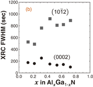
Fig. 1. (a) Lattice constants of AlGaN layers grown on AlN/sapphire templates determined by XRD measurements (solid circles). The solid line between GaN and AlN represents the lattice constants of completely relaxed AlGaN crystals following Vegard's law. Dashed lines are iso-composition lines for varying-Al-content AlGaN crystals. (b) XRC FWHM values of (0002) and  reflections for varying-Al-content AlGaN layers.
Download figure:
Standard image High-resolution imageTable I. Physical constants used in this study.30,31)
| Item | InN | GaN | AlN |
|---|---|---|---|
| Intrinsic lattice constants | |||
| a0 (Å)30) | 3.54 | 3.188 | 3.112 |
| c0 (Å)30) | 5.705 | 5.186 | 4.982 |
| Elastic stiffness constants | |||
| C13 (GPa)31) | 70 | 68 | 94 |
| C33 (GPa)31) | 205 | 354 | 377 |
| Spontaneous polarization charge | |||
| PSP (C/m2)31) | −0.042 | −0.034 | −0.09 |
| Piezoelectric constants | |||
| e31 (C/m2)31) | −0.45 | −0.37 | −0.62 |
| e33 (C/m2)31) | 0.81 | 0.67 | 1.50 |
Taking into consideration the lattice constants in the strained AlGaN layers as described above, InAlN/AlGaN heterostructures were then grown to have in-plane lattice-matched structures. Figure 2 shows typical XRD reciprocal space maps (RSMs) obtained around the  reflections for the MOCVD-grown InAlN/AlGaN heterostructures. As seen in these figures, the x-coordinates of the reflections from the InAlN layers were almost perfectly consistent with those from the underlying AlGaN layers, which confirms that the InAlN barrier layers had almost the same a-axis lengths as those in the underlying AlGaN channel layers. To verify the lattice consistency of these structures more accurately, the evaluation of the lattice strain was required. Table II shows the estimated strains in the InAlN barrier layers of the nearly lattice-matched heterostructures, which were calculated using Eq. (1) with the constants listed in Table I. As confirmed by this table, the InyAl1−yN layers with y values of 0.14, 0.12, and 0.10 were almost lattice-matched to the underlying AlxGa1−xN layers with x values of 0.1, 0.21, and 0.34, respectively, with less strain within 0.1%.
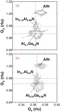
Fig. 2. XRD RSMs obtained around  reflections for (a) In0.14Al0.86N/Al0.1Ga0.9N and (b) In0.1Al0.9N/Al0.34Ga0.66N heterostructures. Qx and Qy are the reciprocal lattice vectors in the [0001] and
 ![$[10\bar{1}0]$](https://content.cld.iop.org/journals/1882-0786/8/2/021001/revision1/AP141235if005.gif) directions, respectively, with units in rlu (1 rlu = 1/d Å−1, where d represents the lattice spacing).
directions, respectively, with units in rlu (1 rlu = 1/d Å−1, where d represents the lattice spacing).
Download figure:
Standard image High-resolution imageTable II. Measured lattice constants (a- and c-axes), in-plane lattice strain (εxx), and out-of-plane lattice strain (εzz) in InyAl1−yN barrier layers with y values of 0.14, 0.12, and 0.1 grown on AlxGa1−xN layers with x values of 0.10, 0.21, and 0.34, respectively.
| x in AlxGa1−xN channel layers | Characterization results of InyAl1−yN barrier layers | ||||
|---|---|---|---|---|---|
| y | a-axis (Å) | c-axis (Å) | εxx (%) | εzz (%) | |
| 0.10 | 0.14 | 3.173 | 5.090 | 0.02 | −0.01 |
| 0.21 | 0.12 | 3.163 | 5.081 | 0.02 | −0.01 |
| 0.34 | 0.10 | 3.153 | 5.062 | −0.09 | 0.04 |
In order to characterize the 2DEG properties in the InAlN/AlGaN heterostructures, C–V and Hall effect measurements were conducted. Figure 3 shows the results of the C–V depth profiling, which indicates that the electrons were highly concentrated at a depth of approximately 10–12 nm from the surfaces, and that the electron density (Nc-v) decreased abruptly in the depth direction. This confirms that highly concentrated 2DEGs were generated at the heterointerfaces. Table III shows the results of the room-temperature Hall effect measurements, which revealed that the 2DEG densities were higher than 2 × 10¹³/cm2 for all samples. On the other hand, the 2DEG mobilities were found to be much lower than those of conventional AlGaN/GaN 2DEG heterostructures. This can be considered to be due to the strong effect of the alloy disorder scattering in the AlGaN channel. As a result, the sheet resistance increased from 1,267 to 1,919 Ω/sq with the increase in Al content in the AlGaN channel layers. To evaluate the validity of the measured 2DEG densities, we estimated the total amount of electric charge at the heterointerfaces by considering the spontaneous and piezoelectric polarization effects in the InAlN/AlGaN heterostructures, and compared the estimated amount of electrical charge with the measured one. The spontaneous polarization charge PSP in the ternary AlGaN and InAlN alloys was linearly interpolated using the constants of binary III–nitrides listed in Table I. The piezoelectric polarization charge PEP was calculated according to34)

where e31 and e33 are the piezoelectric constants, which are also listed in Table I. Here, the εxx of −0.3% in the AlGaN channel layers was taken into account, while the strain in the InAlN barrier layers was neglected because of the lower values. In this study, the effect of the surface barrier height was not considered. The calculated results are shown in Table III, which indicates that the measured 2DEG densities are in good agreement with the calculated values. It was thus confirmed that the high-density 2DEGs in the nearly lattice-matched InAlN/AlGaN heterostructures can be explained as being the result of internal polarization effects. Finally, Fig. 4 shows the relationship between the 2DEG density and mobility for the InAlN/AlGaN heterostructures. Here, the results reported for AGaN-channel heterostructures with AlGaN barriers6,8,11,15) and an AlN barrier16) are also plotted. As seen in this figure, the InAlN/AlGaN heterostructures grown in this study were found to have higher 2DEG densities than and almost the same sheet resistance as other AlGaN-channel heterostructures.
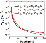
Fig. 3. Depth profiling of 2DEGs in nearly lattice-matched InAlN/AlGaN heterostructures obtained by C–V measurement.
Download figure:
Standard image High-resolution image
Fig. 4. Relationship between the measured 2DEG densities and mobilities for nearly lattice-matched InAlN/AlGaN heterostructures. The results previously reported for AGaN-channel heterostructures with AlGaN barriers6,8,11,15) and with an AlN barrier16) are also plotted. Dashed lines represent constant sheet resistance lines.
Download figure:
Standard image High-resolution image
Table III. Room-temperature 2DEG density (Ns), mobility (μ), and sheet resistance (Rsh) values of nearly lattice-matched InAlN/AlGaN heterostructures obtained by Hall effect measurements, and calculated 2DEG density (Ns,calc) values derived from the total amount of electric charge from the spontaneous (PSP) and piezoelectric polarization (PPE) charges in the respective heterostructures.
| Sample structure | Results of Hall effect measurements | Calculated results | |||||
|---|---|---|---|---|---|---|---|
| Ns (cm−2) | μ (cm2 V−1 s−1) | Rsh (Ω/sq.) | PSP (C/m2) | PPE (C/m2) | PSP + PPE (C/m2) | Ns,calc (cm−2) | |
| In0.14Al0.86N/Al0.1Ga0.9N | 3.0 × 10¹³ | 165 | 1,267 | −0.043 | −0.003 | −0.046 | 2.9 × 10¹³ |
| In0.12Al0.88N/Al0.21Ga0.79N | 2.8 × 10¹³ | 162 | 1,477 | −0.038 | −0.004 | −0.042 | 2.6 × 10¹³ |
| In0.1Al0.9N/Al0.34Ga0.66N | 2.5 × 10¹³ | 130 | 1,919 | −0.033 | −0.004 | −0.036 | 2.3 × 10¹³ |
In summary, InAlN/AlxGa1−xN (x = 0.1, 0.21, and 0.34) heterostructures with a 1-nm-thick AlN interfacial layer were grown on AlN/sapphire templates by MOCVD. XRD analyses confirmed that the InAlN barrier layers were nearly lattice-matched to the AlGaN channel layers with less strain. C–V and Hall effect measurements revealed that 2DEGs with high densities exceeding 2 × 10¹³/cm2 were generated at the heterointerface for all samples. The sheet resistance increased from 1,267 to 1,919 Ω/sq. with the increase in Al content in the AlGaN channel, owing to decreases in 2DEG density and mobility. In comparison with AlGaN-channel heterostructures ever reported, InAlN/AlGaN heterostructures showed higher 2DEG densities with almost comparable sheet resistances.
Acknowledgment
This work was partially supported by the Super Cluster Program of the Japan Science and Technology Agency (JST).