
Abstract
The "type-II" staggered band lineup at the base-collector junction of InP/GaAsSb double-heterojunction bipolar transistors (DHBTs) eliminates the current blocking effect observed in InP/GaInAs DHBTs and allows the use of a pure binary InP collector that provides a high breakdown voltage and good thermal conductivity. Improvement of the power gain cutoff frequency fMAX requires a reduction in base resistance and/or base-collector capacitance. We have decreased the base contact resistivity by in situ Ar sputtering immediately prior to the base contact deposition. The resulting DHBTs simultaneously feature fT = 429 GHz and fMAX = 715 GHz. To the best of the authors' knowledge, this is the highest reported fMAX for InP/GaAsSb-based DHBTs to date.
Export citation and abstract BibTeX RIS
InP/GaAsSb double-heterojunction bipolar transistors (DHBTs) were developed as an alternative to InP/GaInAs DHBTs for applications in high-speed electronic systems.1) The staggered band alignment at InP/GaAsSb heterojunctions enables the use of a simplified device structure with a pure InP collector layer, providing good thermal conductivity and high breakdown voltages.2–4) GaAsSb-based DHBTs have demonstrated fT × BVCEO products as high as 2.5 THz·V,2) as well as fT and fMAX in excess of 600 GHz.2,4) InP/GaAsSb DHBTs are thus promising candidates for next-generation sub-millimeter-wave integrated circuits. Further improvement of the maximum oscillation frequency requires a reduction in the base-collector junction capacitance and/or base resistance. We have decreased the base contact resistivity by in-situ Ar sputtering immediately prior to the base contact deposition. Devices with an emitter area of 0.3 × 4.4 µm2 simultaneously show the maximum oscillation frequency fMAX = 715 GHz and the current gain cutoff frequency fT = 429 GHz. To date, this is the highest reported fMAX achieved with InP/GaAsSb DHBTs.
The DHBT epitaxial layer structure was grown by metal organic chemical vapor deposition (MOCVD) on 2 in. semi-insulating InP substrates. The subcollector consists of a 300-nm-thick InP:S buffer layer doped at 2.2 × 1019 cm−3, a 20-nm-thick Ga0.40In0.60As:Si etch stop layer doped at 3.0 × 1019 cm−3, and a 50-nm-thick InP:S pedestal layer doped at 2.2 × 1019 cm−3. The purpose of the InP pedestal is to reduce the extrinsic collector capacitance by increasing the mesa height.5) The 125-nm-thick InP:S collector is nominally doped at 1.3 × 1017 cm−3. The 20-nm-thick GaAsxSb1−x base is compositionally graded from x = 0.41 on the collector side to x = 0.59 on the emitter side.6) The average base doping density is 8.4 × 1019 cm−3, resulting in Rsh = 1077 Ω/□.
The composite InP/GaInP emitter is doped at a level of 2.5 × 1016 cm−3, and consists of a 15-nm-thick GayIn1−yP:Si layer and a 5-nm-thick InP:Si layer.7–9) The first 5 nm of the ternary alloy has y = 0.22, which is followed by a grading to y = 0 over 10 nm. The composite emitter is followed by a 130-nm-thick InP:Si emitter layer doped at 1.5 × 1019 cm−3. The 35-nm-thick emitter contact layer is doped at 3.8 × 1019 cm−3 and consists of 20 nm of Ga0.47In0.53As, followed by 10 nm of Ga0.47In0.53As graded to Ga0.25In0.75As, and 5 nm of Ga0.25In0.75As. Transmission line measurements indicate emitter and collector contact resistivities of 2.0 and 1.3 Ω µm2, respectively.
The transistors were fabricated by a standard triple mesa process with 0.4-µm-wide emitter and base electrodes defined by electron beam lithography.10) The emitter mesa was formed by a combination of inductively coupled plasma (ICP) and wet etching, resulting in an emitter-base junction area of 0.3 × 4.4 µm2. The emitter and base electrodes consist of electron-beam-evaporated Ti/Pt/Au and Pd/Ni/Pt/Au metal stacks, respectively. The GaAsSb base surface was in situ sputtered with Ar ions prior to the deposition of the base metal stack. The Ar sputtering removes about 10 nm of the GaAsSb layer (including the natural oxide) in the base contact area, thereby improving the contact interface quality.11–13) TLM measurements show an improved base contact resistivity with increasing sputtering time, as shown in Fig. 1. For sufficiently long sputtering times, the contact resistivity reaches 10−9 Ω·cm2, which is a clear improvement over the standard process. Because the emitter contact acts as a mask for the Ar sputtering, the gap region between the base contact and the emitter mesa is not etched, as illustrated in Fig. 2(a). The emitter sidewall and the base surface were passivated using plasma-enhanced chemical-vapor-deposited silicon nitride. A low-temperature Teflon-based etch-back process was utilized for planarization prior to the deposition of the probe pad metal.10) Figure 2(b) shows an SEM image of the focused ion beam cross section of a finalized DHBT. The Teflon film rapidly degrades under electron and ion beam irradiation and is therefore only partially visible and indicated by the arrow in Fig. 2(a).
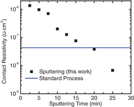
Fig. 1. Base contact resistivity vs Ar sputtering time determined from TLM measurements. The solid line indicates the contact resistivity resulting from the standard base contact formation process.
Download figure:
Standard image High-resolution image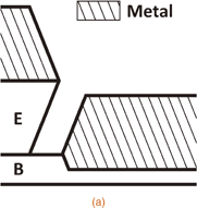
Download figure:
Standard image High-resolution image
Fig. 2. (a) Schematic representation of emitter and base contact. The emitter contact acts as a mask for the Ar sputtering and protects the base access region. (b) SEM image of FIB cross section of a representative DHBT. The arrow indicates residuals of the Teflon planarization.
Download figure:
Standard image High-resolution imageFigure 3 shows the Gummel characteristics of a device with a 0.3 × 4.4 µm2 emitter area. The base and collector current ideality factors are nB = 1.53 and nC = 1.04, respectively. The peak common-emitter current gain is β = 11 with VBC = 0 V. The common-emitter current–voltage characteristics are shown in the inset of Fig. 3. The common-emitter breakdown voltage BVCEO is more than 5 V at the collector current density JC = 1 kA/cm2.
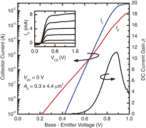
Fig. 3. Gummel characteristics of a DHBT with an emitter area of 0.3 × 4.4 µm2. Inset: Common-emitter current–voltage characteristic of the same device.
Download figure:
Standard image High-resolution imageRF performance was characterized from 0.2 to 40.2 GHz using an HP8510C vector network analyzer calibrated with the line-reflect-reflect-match technique using off-wafer standards. The probe pad parasitics were de-embedded in accordance with the method presented by Koolen et al.14) using on-wafer open/short test structures with the same layout as the device pads. Figure 4 shows the short-circuit current gain |h21|2 and Mason's unilateral power gain U for the device shown in Fig. 4 biased at VCE = 1.6 V and IC = 10.5 mA. The dependences of fT and fMAX on the collector current for VCE = 1.2 and 1.6 V are also shown in the inset of Fig. 4. Determination of the cutoff frequencies by single-pole transfer function fits over the full measurement range results in fT = 442 GHz and fMAX = 701 GHz. A higher VCE of 1.6 V yields fT = 429 GHz and fMAX = 715 GHz. The small-signal equivalent circuit model extracted from forward-active mode and open-collector S-parameter measurements is shown in Fig. 5 (top) for VCE = 1.6 V and IC = 10.5 mA.15) The simulated small-signal equivalent circuit S-parameters agree well with the measured values, as shown in Fig. 5 (bottom).

Fig. 4. Extrapolation of fMAX and fT by single-pole transfer function fits. Inset: Dependences of fT and fMAX on collector current at VCE = 1.2 and 1.6 V.
Download figure:
Standard image High-resolution image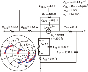
Fig. 5. Small-signal equivalent circuit (top) and Smith chart showing the measured and simulated transistor S-parameters (bottom).
Download figure:
Standard image High-resolution image
For a given current gain cutoff frequency fT, the maximum oscillation frequency fMAX is determined by the base-collector capacitance and base resistance16) as follows:

The present record fMAX > 700 GHz was achieved by decreasing the base contact resistivity. Compared with our standard process, we observe a reduction in the (CBCRB)eff time constant by a factor of two. Assuming that all other components remain unchanged, we calculate a fourfold reduction in the base contact resistance owing to the Ar sputtering, which is in general agreement with the TLM results shown in Fig. 1. The present devices show a ∼100 GHz higher fMAX than those previously reported with the same epitaxial layer structure.4)
In conclusion, we have demonstrated the first InP/GaAsSb DHBTs with an fMAX exceeding 700 GHz. Devices with a 0.3 × 4.4 µm2 emitter area have a DC gain β = 11 and a high breakdown voltage BVCEO > 5 V.
Acknowledgments
The authors would like to thank the staff of FIRST Lab at ETH Zurich, Zurich, Switzerland, for their support. This work was partially supported by ETH through ETHIIRA 16-11-1.