
Abstract
TiO2/CH3NH3PbI3-based photovoltaic devices were fabricated. The microstructures of these devices were investigated by X-ray diffraction, transmission electron microscopy, and their calculations. Structure analysis indicated phase transformation of the perovskite structure from a tetragonal to a cubic system by annealing, which resulted in the improvement of photovoltaic properties of the devices. Effects of a multiple spin-coating method using a mixture solution were also investigated. The result showed an increase in the efficiencies of the devices, due to the microstructural change of the perovskite compound layers.
Export citation and abstract BibTeX RIS
Recently, organic–inorganic hybrid solar cells with perovskite-type pigments have been heavily studied.1–5) Organic solar cells with a CH3NH3PbI3 compound that has a perovskite structure have high conversion efficiencies and stability.6–8) Since achieving a photoconversion efficiency of 15%,9) efficiencies as high as 19.3%10) have been reported for various device structures and processes.11–14) The photovoltaic properties of solar cells are strongly dependent on the fabrication process, hole transport layers, electron transport layers, nanoporous layers, interfacial microstructures, and crystal structures of the perovskite compounds. In particular, the crystal structures of the perovskite-type compounds strongly affect the electronic structures, such as energy band gaps and carrier transport, and a detailed analysis of them is imperative.
The purpose of the present work is to investigate microstructures and photovoltaic properties of photovoltaic devices with perovskite-type CH3NH3PbI3 compounds, TiO2 electron transport layers, and 2,2',7,7'-tetrakis(N,N-di-pmethoxyphenylamine)-9,9'-spirobifluorene (spiro-OMeTAD) hole-transport layers (HTL), which were prepared by a simple spin-coating technique. Effects on the microstructures and photovoltaic properties of annealing and multiple spin-coating of perovskite compounds were investigated by X-ray diffraction (XRD), transmission electron microscopy (TEM), current density–voltage (J–V) curves, and incident photon-to-current conversion efficiency (IPCE). TEM is a powerful tool for structure analysis of solar cells15) and perovskite-type structures at the atomic scale.16,17)
A schematic illustration of the fabrication of the present TiO2/CH3NH3PbI3 photovoltaic cells is shown in Fig. 1. The details of the fabrication process are described in the reported paper9,18) except for the mesoporous TiO2 layer.19) The 0.30 M TiOx precursor solution was prepared from titanium diisopropoxide bis(acetyl acetonate) (Sigma Aldrich, 0.55 µL, 0.11 mL) with 1-butanol (1 mL), then spin-coated on the F-doped tin oxide (FTO) substrate and annealed at 125 °C for 5 min. This process was performed two times, and the FTO substrate was sintered at 500 °C for 30 min to form the compact TiO2 layer. After that, mesoporous TiO2 paste was coated on the substrate by spin-coating. For the mesoporous TiO2 layer, the TiO2 paste was prepared with TiO2 powder (Aerosil P-25) with poly(ethylene glycol) (Nacalai tesque, PEG #20000) in ultrapure water. The solution was mixed with acetylacetone (10.0 µL) and triton X-100 (Sigma Aldrich, 5 µL) for 30 min. The cells were annealed at 120 °C for 5 min and at 500 °C for 30 min. CH3NH3I was synthesized by reacting 23.2 mL of methylamine (CH3NH2, Tokyo Chemical Industry) and 25.0 mL of hydroiodic acid at 0 °C for 2 h with stirring. Then dried using a rotary evaporator at 60 °C for 3 h. The obtained CH3NH3I was then dried in a vacuum. For the preparation of pigment with a perovskite structure, a solution of CH3NH3I (98.8 mg) and PbI2 (Sigma Aldrich, 289.3 mg) with a mole ratio of  in γ-butyrolactone (Nacalai Tesque, 0.5 mL) was mixed at 60 °C. The solution of CH3NH3PbI3 was then introduced into the TiO2 mesopores by a multiple spin-coating method and annealed at 100 °C for 15 min. The specimen was dried and cooled in air for a few seconds between the multiple spin-coatings to avoid the re-dissolution of the pre-coated layer. Then, the HTL was prepared by spin-coating. To create the HTLs, a solution of spiro-OMeTAD (Wako Pure Chemical Industries, 36.1 mg) in chlorobenzene (0.5 mL) was mixed with a solution of lithium bis(trifluoromethylsulfonyl) imide (Li-TFSI, Tokyo Chemical Industry, 260 mg) in acetonitrile (0.5 mL) for 12 h. The former solution with 4-tert-butylpyridine (14.4 µL) was mixed with the Li-TFSI solution (8.8 µL) for 30 min at 70 °C. All procedures were carried out in air. Finally, gold (Au) metal contacts were evaporated to form top electrodes. Layered structures of the present photovoltaic cells were denoted as FTO/TiO2/CH3NH3PbI3/spiro-OMeTAD/Au, as shown in a schematic illustration in Fig. 1.
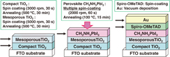
Fig. 1. Schematic illustration for the fabrication of photovoltaic cells using CH3NH3PbI3 and TiO2.
Download figure:
Standard image High-resolution imageThe J–V characteristics of the photovoltaic cells were measured under illumination at 100 mW cm−2 by using an AM 1.5 solar simulator. The solar cells were illuminated through the side of the FTO substrates, and the illuminated area was 0.16 cm2. The IPCE of the cells was also investigated (Enli Technology QE-R). The microstructures of the thin films were investigated by using an X-ray diffractometer (Bruker D2 PHASER) and a transmission electron microscope (Hitachi H-8100) operated at 200 kV.
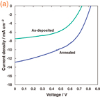
The J–V characteristics of the TiO2/CH3NH3PbI3/spiro-OMeTAD photovoltaic cells under illumination are shown in Fig. 2(a), which indicates an annealing effect of the CH3NH3PbI3 layer. The as-deposited CH3NH3PbI3 cell provided a conversion efficiency of 2.83%. The CH3NH3PbI3 cell annealed at 100 °C for 15 min provided better photovoltaic properties compared with the as-deposited one, as listed in Table I. The highest efficiency was obtained for the annealed CH3NH3PbI3 cell, which provided a power conversion efficiency (η) of 5.16%, a fill factor (FF) of 0.486, a short-circuit current density (JSC) of 12.9 mA cm−2, and an open-circuit voltage (VOC) of 0.827 V. Figure 2(b) shows results of multiple spin-coating of CH3NH3PbI3, which will be described later.
Download figure:
Standard image High-resolution image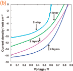
Fig. 2. J–V characteristic of TiO2/CH3NH3PbI3 photovoltaic cells. (a) As-deposited and annealed samples. (b) CH3NH3PbI3 layers prepared by multiple spin-coating.
Download figure:
Standard image High-resolution imageTable I. Measured photovoltaic parameters of TiO2/CH3NH3PbI3 cells before and after annealing.
| Sample | JSC (mA cm−2) | VOC (V) | FF | η (%) |
|---|---|---|---|---|
| As-deposited | 7.50 | 0.730 | 0.517 | 2.83 |
| Annealed | 12.9 | 0.827 | 0.486 | 5.16 |
XRD patterns of CH3NH3PbI3 thin films on the glass substrate before and after annealing are shown in Fig. 3(a). The diffraction peaks can be indexed by tetragonal and cubic crystal systems for as-deposited and annealed films, respectively. Although the as-deposited film is a single perovskite phase, broader diffraction peaks due to a PbI2 compound appeared after annealing, as shown in Fig. 3(a). Figures 3(b) and 3(c) are enlarged XRD patterns at 2θ of ∼14 and ∼28°, respectively. Split diffraction peaks of 002–110 and 004–220 for the as-deposited sample changed into diffraction peaks of 100 and 200 after annealing, which indicates the structural transformation from the tetragonal to cubic crystal system.

Fig. 3. (a) XRD patterns of CH3NH3PbI3 thin films before and after annealing. Enlarged XRD patterns at 2θ of (b) ∼14° and (c) ∼28°.
Download figure:
Standard image High-resolution imageThe CH3NH3PbI3 crystals have perovskite structures and provide structural transitions from a tetragonal to a cubic system upon heating at ∼330 K,20–22) as shown in the structure models of Figs. 4(a) and 4(b). Although the CH3NH3PbI3 perovskite crystal has a cubic symmetry for the highest temperature phase, the CH3NH3 ion is polar and has C3v symmetry, which results in a disordered cubic phase.23,24) In addition to the disordering of the CH3NH3 ion, the iodine (I) ions are also disordered in the cubic phase, as shown in Fig. 4(a). Site occupancies were set as 1/4 for I and 1/12 for C and N. The CH3NH3 ion occupies 12 equivalent orientations of the C2 axis, and hydrogen atoms have two kinds of configurations on the C2 axis.22) As the temperature decreased, the cubic phase was transformed into the tetragonal phase, and I ions became ordered, which resulted in a lower symmetry than in the cubic phase, as shown in Fig. 4(b). Site occupancies were set as 1/4 for C and N for the tetragonal CH3NH3PbI3. For the high temperature phase, unit cell volume of the cubic structure is 261.0 Å3, which is bigger than that of the tetragonal structure (245.6 Å3), as listed in Table II. This would be due to both thermal expansion of the unit cell and atomic disordering of I in the cubic phase. As the temperature lowers, the tetragonal phase is transformed into the orthorhombic systems because of the ordering of CH3NH3 ions in the unit cell.25) Calculated XRD patterns of the CH3NH3PbI3, with cubic and tetragonal structures based on the structure models of Figs. 4(a) and 4(b), are shown in Fig. 4(c), and the full width at half maximum was set as 0.10. The calculated XRD pattern indicates splitting of diffraction reflections of 100 to 002/110 by reduction of crystal symmetry from the cubic to the tetragonal phase.

Fig. 4. Structure models of CH3NH3PbI3 with (a) cubic and (b) tetragonal crystals along perspective view. (c) Calculated XRD patterns of CH3NH3PbI3 with cubic and tetragonal structures.
Download figure:
Standard image High-resolution imageTable II. Measured and reported structural parameters of CH3NH3PbI3. V: unit cell volume. Z: number of chemical units in the unit cell.
| Sample | Crystal system | Lattice constants (Å) | V (Å3) | Z | V/Z (Å3) |
|---|---|---|---|---|---|
| As-deposited | Tetragonal | a = 8.8620 | 993.10 | 4 | 248.27 |
| c = 12.6453 | |||||
| Annealed | Cubic | a = 6.2724 | 246.78 | 1 | 246.78 |
| Ref. 24 (220 K) | Tetragonal | a = 8.800 | 982.33 | 4 | 245.6 |
| c = 12.685 | |||||
| Ref. 23 (330 K) | Cubic | a = 6.391 | 261.0 | 1 | 261.0 |
The XRD results in Fig. 3 indicated phase transformation of the CH3NH3PbI3 perovskite structure from the tetragonal to the cubic system by partial separation of PbI2 from the CH3NH3PbI3 phase during annealing, which corresponds to the decrease of the unit cell volume of the perovskite phase from 248.27 to 246.78 Å3, as listed in Table II. In addition to the I atoms, Pb atoms might also be disordered, and site occupancies of Pb atoms would be less than 1. It should be noted that the structure transition from the tetragonal to the cubic structure in the present work is due to the partial separation of PbI2 from the CH3NH3PbI3 phase, which is different from the ordinary tetragonal–cubic transition at 330 K.20,21)
Figures 5(a) and 5(b) are a TEM image and an electron diffraction pattern of TiO2/CH3NH3PbI3, respectively. The TEM image shows TiO2 nanoparticles with sizes of ∼50 nm, and the polycrystalline CH3NH3PbI3 phase shows dark contrast, which is due to Pb having the largest atomic number in the present materials. The electron diffraction pattern of Fig. 5(b) shows the Debye–Scherrer rings from the nanocrystalline TiO2 particles, which are indexed as the 101, 004, and 200 spacings of the anatase TiO2. The thickness of the mesoporous TiO2 layer was measured to be ∼300 nm by using atomic force microscopy. In addition to the Debye–Scherrer rings, diffraction spots corresponding to the CH3NH3PbI3 crystal with a cubic structure23) were observed and indexed, as shown in Fig. 5(b). Other diffraction spots, except for the Debye–Scherrer rings of TiO2, are also from the CH3NH3PbI3 nanoparticles. A structure model and its calculated electron diffraction pattern of a cubic CH3NH3PbI3 phase projected along the [210] direction are shown in Figs. 5(c) and 5(d), respectively. The calculated electron diffraction pattern agrees well with the observed pattern of Fig. 5(b).
Fig. 5. (a) TEM image and (b) electron diffraction pattern of TiO2/CH3NH3PbI3. "P" indicates CH3NH3PbI3 perovskite phase. (c) Structure model and (d) its calculated electron diffraction pattern of cubic CH3NH3PbI3 projected along the [210] direction.
Download figure:
Standard image High-resolution imageThe J–V characteristics of the TiO2/CH3NH3PbI3/spiro-OMeTAD photovoltaic cells prepared by multiple spin-coating of CH3NH3PbI3 are shown in Fig. 2(b). Figure 2(b) indicates the effect of spin-coating times of CH3NH3PbI3 on the photovoltaic properties, and the detailed parameters of the best device are listed in Table III. The highest efficiency was obtained for the cell that was spin-coated for four times, which provided an η of 6.96%, an FF of 0.496, a JSC of 16.5 mA cm−2, and a VOC of 0.848 V. Further spin-coating lowered the efficiencies of the cells, as shown in Fig. 2(b). Although 2-step deposition6) (spin-coating PbI2 and dipping in the CH3NH3I solution) was also performed in air, the efficiency was lower compared with that by multiple spin-coating, as observed in Fig. 2(b) and Table III.
Table III. Measured photovoltaic parameters of TiO2/CH3NH3PbI3 cells with various numbers of CH3NH3PbI3 layers.
| Number of layers | JSC (mA cm−2) | VOC (V) | FF | η (%) |
|---|---|---|---|---|
| 1 | 13.1 | 0.793 | 0.413 | 4.29 |
| 2 | 15.8 | 0.860 | 0.400 | 5.44 |
| 4 | 16.5 | 0.848 | 0.496 | 6.96 |
| 6 | 15.7 | 0.802 | 0.500 | 6.30 |
| 10 | 16.0 | 0.721 | 0.493 | 5.69 |
| 2-step | 10.4 | 0.604 | 0.534 | 3.35 |
Figure 6(a) shows XRD patterns of TiO2/CH3NH3PbI3 cells that were spin-coated with CH3NH3PbI3 layers for one or four times. Enlarged XRD patterns of the 100 reflection of the cubic structure are shown in Fig. 6(b). The 100 reflection of 4-layers was shifted to a lower angle and broadened compared with the cell prepared by 1-time spin coating. The lattice parameters of the CH3NH3PbI3 for 1 and 4 layers are 6.3049 and 6.3222 Å, respectively, which indicates lattice expansion of the unit cell. On the other hand, the crystallite sizes for 1 and 4 layers are 52.0 and 43.3 nm, respectively. It is believed that the CH3NH3PbI3 phase was stuffed in pores inside of the mesoporous TiO2 layer during the 1- or 2-times spin-coating. After the pores inside of the mesoporous TiO2 were fully filled with the perovskite phase, the perovskite-only layer would be formed on the mesoporous TiO2 layer for 3- or 4-times spin-coating, which provided the highest efficiency. A Decrease in crystallite size due to spin-coating indicates that the grain growth of the perovskite phase might be enhanced in the mesoporous TiO2.

Download figure:
Standard image High-resolution image
Fig. 6. (a) XRD patterns of TiO2/CH3NH3PbI3 cells prepared by 4-times spin-coating. (b) Enlarged patterns of (a) at 2θ of ∼14°.
Download figure:
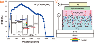
Standard image High-resolution imageThe IPCE spectrum of the photovoltaic cell with the TiO2/CH3NH3PbI3/spiro-OMeTAD structure is shown in Fig. 7(a). The measurement region is in the range of 300 to 900 nm, and the perovskite CH3NH3PbI3 structure exhibits photo-conversion efficiencies between 300 and 800 nm, which almost agrees with the reported energy gaps of 1.5125) and 1.61 eV26) (corresponding to 821 and 770 nm, respectively) for the CH3NH3PbI3 phase. This indicates that excitons and/or free charges would be effectively generated in the perovskite layers upon illumination by light.
Fig. 7. (a) IPCE spectrum and energy level diagrams of TiO2/CH3NH3PbI3 cell. (b) Model of interfacial.
Download figure:
Standard image High-resolution image
From the TEM results, size distributions of TiO2 nanoparticles were observed, indicating a microcrystalline structure, as shown in Fig. 7(b), and there seems to be no special crystallographic relation at the interface. The interface between the TiO2 and CH3NH3PbI3 phases would not be perfectly connected over the large area. The cell prepared by 4-times spin-coating provided the highest efficiency, which would have an interfacial microstructure as shown in Fig. 7(b). For the cell prepared by 10-times spin coating, layer thickness of the CH3NH3PbI3 phase was too large, which resulted in an increase in the inner electronic resistance and decrease in the efficiency, as listed in Table III.
An energy level diagram of TiO2/CH3NH3PbI3 photovoltaic cells is summarized as shown in Fig. 7(a). Previously reported values were also used for the energy levels of the figures by adjusting them to the present work.1,15) An energy barrier would exist at the semiconductor metal interface.27) The electronic charge generation is caused by light irradiation from the FTO substrate side. The TiO2 layer receives the electrons from the CH3NH3PbI3 crystal, and the electrons are transported to the FTO. The holes are transported to an Au electrode through spiro-OMeTAD. Experimental evidence for photogenerated free carriers, which would enhance the carrier transport, was reported.28) In the present work, the samples were prepared in air, which may result in the reduction of the photo- and thermal stability. Perovskite crystals with higher quality should be prepared in further works.
In conclusion, the structure analysis of TiO2/CH3NH3PbI3 indicated phase transformation of the perovskite structure from the tetragonal to the cubic system by partial separation of PbI2 from the CH3NH3PbI3 phase during annealing, which was confirmed by reduction of the unit cell volume of the perovskite phase and resulted in the improvement of photovoltaic properties of the devices. Effects of a multiple spin-coating method were also investigated, which increased the efficiency to 6.96% for the 4-times spin-coating. This improvement would be due to the perfect coverage and optimum thickness of the perovskite phase on the porous TiO2 layer. Moreover, the lattice constant and crystallite size of the CH3NH3PbI3 increased and decreased, respectively, which indicates the microstructural difference of the perovskite phase between the inside of and above the porous TiO2.