
Abstract
We demonstrate the three-dimensional imaging of threading screw dislocations (TSDs), threading edge dislocations (TEDs), and basal plane dislocations (BPDs) in 4H-SiC using two-photon-excited band-edge photoluminescence. Three-dimensional images of TSDs, TEDs, and BPDs are obtained successfully as dark contrasts on a bright background of band-edge emission. Dislocation images extending ∼200 µm from the surface are demonstrated. The tilt angles of TSDs and TEDs in 4H-SiC epilayers are also measured, and the mechanisms governing the line directions of TEDs and TSDs are discussed.
Export citation and abstract BibTeX RIS
The presence of extended defects hinders the extensive commercialization of 4H silicon carbide (SiC) power devices, which can improve the efficiency of power conversion systems for various applications. Threading screw dislocations (TSDs), threading edge dislocations (TEDs), and basal plane dislocations (BPDs) in 4H-SiC are major dislocations that can significantly impair the performance of the device.1–3) Grazing incidence X-ray topography4,5) and photoluminescence (PL) imaging6–13) are utilized to investigate these dislocations. Although these methods are useful for nondestructive defect analysis, they provide two-dimensional (2D) images with low depth resolution; thus, advanced three-dimensional (3D) imaging methods are expected to be used for investigating the formation and propagation of dislocations. In particular, very high voltage SiC power devices with a thick epilayer require defect imaging as deep as 100–200 µm. X-ray microbeam 3D topography has been successfully applied for the imaging of TSDs,14) BPDs, and TEDs,15,16) although this technique requires a large-scale synchrotron radiation facility.
We have reported that second-harmonic generation (SHG) and two-photon-excited photoluminescence (2PPL) imaging techniques, which can be performed using a multiphoton microscope in individual laboratories, are powerful tools for the 3D analysis of extended defects in 4H-SiC epilayers.17,18) The 3D imaging of 3C inclusions, 8H stacking faults, and single Shockley stacking faults (SSFs) in the epilayers has been demonstrated by the SHG or 2PPL imaging technique. However, multiphoton techniques have not been applied to the imaging of TSDs, TEDs, and BPDs. It is known that band-edge PL emission can show TSDs and TEDs as dark contrasts on a bright background, owing to the quenching of band-edge emissions near defects.11) This study demonstrates how this mechanism can be applied to the 2PPL method for the 3D imaging of TSDs, TEDs, and BPDs in 4H-SiC. Using this method, we analyze the line directions of TEDs and TSDs, and discuss their results in comparison with those previously provided by single-photon-excited photoluminescence (1PPL).12,13)
The samples examined were 8 and 4° off-cut (0001) Si-face 4H-SiC wafers with epilayer thicknesses (tepi) of 26 and 140 µm, respectively. A multiphoton excitation microscopy system (Nikon A1MP series) was used for 2PPL imaging. The excitation laser was a Ti:sapphire mode-locked laser, and the 2PPL was measured with an excitation wavelength (λ1) of 700 nm. The laser beam was focused by a ×20 [numerical aperture (NA) = 0.45] or ×50 (NA = 0.8) magnification objective lens to create an excitation volume19) in which 2PPL occurred. The scanning of the focal point yields a 3D image of 2PPL emission. A band-pass filter was used to select the emission wavelength (λ2) observed, and the intensity of emitted light was measured using a non-descanned detector.20) Owing to the high refractive index of 4H-SiC (nSiC = 2.62), the 3D images obtained were expanded depthwise with a magnification of 3.2 or 3.6 for the ×20 or ×50 objective lens, respectively. The measurement system is further described in detail elswhere.17)
The 2PPL measurement provides a number of horizontal section images stacked depthwise. For each of the targeted threading dislocations, tilt angles from the surface normal toward the step-flow ![$[11\bar{2}0]$](https://content.cld.iop.org/journals/1882-0786/7/12/121303/revision1/AP141071if001.gif) and
and ![$[\bar{1}100]$](https://content.cld.iop.org/journals/1882-0786/7/12/121303/revision1/AP141071if002.gif) directions (TX and TY angles, respectively) were investigated. We also measured TX angles of threading dislocations by cross-sectional 1PPL imaging for a
directions (TX and TY angles, respectively) were investigated. We also measured TX angles of threading dislocations by cross-sectional 1PPL imaging for a  section of a thin bar-shaped specimen cut out from a 4H-SiC wafer.12,13)
Figure 1 shows the results of 2PPL band-edge emission imaging for TSDs and TEDs in comparison with grazing incidence X-ray topography. The sample used was a 4° off-cut epitaxial wafer (tepi = 140 µm). The X-ray topography image ( ) is shown in Fig. 1(a), where TSDs and TEDs are identified by the appearance of each defect contrast5) and indicated by broken circles and small arrows, respectively. The 2PPL 3D imaging was performed using a band-pass filter at 387 ± 8 nm, and a horizontal 2PPL section image for an area identical to that in Fig. 1(a) is shown in Fig. 1(b). The band-edge emission image exhibits dark spots, which correlate perfectly with the defect contrasts of TSDs and TEDs in the X-ray topography image. The dark spots corresponding to TSDs are larger than those corresponding to the TEDs [Fig. 1(b)], showing that carrier recombination is further enhanced in TSDs than in TEDs.11) However, the difference between the sizes of the dark spots is less conspicuous than the defect contrast in the X-ray topography. The sectional 2PPL image along the cs1 cross section [Fig. 1(b)] is shown in Fig. 1(c), which clearly exhibits the propagation of a TSD from the 200-µm-deep level (substrate region) to the surface, penetrating the 140-µm-thick epilayer. The propagation of two TEDs in the epilayer is observable in the 2PPL image along the cs2 cross section [Fig. 1(b)], as shown in Fig. 1(d). We have confirmed that TEDs in a substrate region are also observable by the 2PPL imaging,21) although TED lines in the substrate are not visible in Fig. 1(d). The intensity of 2PPL band-edge emission decreases at deeper levels in the epilayer, which is possibly caused by depth-induced lens aberration.17) The substrate region yields a stronger 2PPL band-edge emission than the epilayer, as shown in the cross-sectional images. Unlike the 2PPL images, high-quality epilayers tend to show a stronger band-edge emission in normal 1PPL measurements. The 2PPL measurement is performed under a very strong excitation given by the focused laser pulse, while the nitrogen doping concentrations are on the orders of 1018 and 1014 cm−3 for the substrate and epilayer, respectively. It is further studied to clarify the relationship between two-photon excitation and band-edge emission intensities for 4H-SiC with different nitrogen doping concentrations. The intensity inversion of the band-edge emission provides the perspective image shown in Fig. 1(e), where the thick arrow indicates the TSD shown in Fig. 1(c). We can visually examine the propagation of a number of threading dislocations using the intensity inversion image, although the dark line contrast is covered by the surrounding bright emission and not visualized in the original uninverted perspective image.
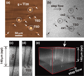
Fig. 1. Results of 3D 2PPL imaging for TSDs and TEDs in 4° off-cut wafers in comparison with grazing incidence X-ray topography. (a) X-ray topography image and (b) horizontal 2PPL section image for the identical area, (c) section image along cs1 cross section in (b), (d) section image along cs2 in (b), and (e) perspective image given by intensity inversion.
Download figure:
Standard image High-resolution imageThe results of 2PPL imaging for a BPD in comparison with X-ray topography are shown in Fig. 2, where an 8° off-cut wafer (tepi = 26 µm) was used. The dark arc of a BPD and three spots of TEDs are found in the X-ray topography image [Fig. 2(a)]. For the identical area, two 3D 2PPL images were obtained with band-pass filters at 387 ± 8 and 428 ± 13 nm. Their horizontal section images overlap in Fig. 2(b), where we can confirm an SSF as a triangle filled by the violet emission (λ2 = 420 nm) and surrounded by dark lines. The horizontal straight line corresponds to a Si-core Shockley partial, while the curved and tilted straight lines correspond to C-core Shockley partials.22) The appearance of the curved dark line matches that of the X-ray topography contrast of the BPD. This means that the Si-core partial composing the original BPD moved during the 2PPL measurement owing to the high injection of excess carriers created by the intense laser illumination, forming a triangular SSF.22) Figure 2(c) shows a sectional 2PPL image along the cs3 cross section [Fig. 2(b)], which exhibits a BPD tilting 8° from the surface and a TED propagating almost normal to the surface.
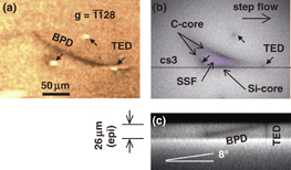
Fig. 2. Results of 2PPL imaging for a BPD in the 8° off-cut wafer in comparison with grazing incidence X-ray topography. (a) X-ray topography image, (b) horizontal 2PPL section image created by overlapping band-edge emission and SSF emission images, and (c) section image along cs3 cross section in (b).
Download figure:
Standard image High-resolution imageFigure 3(a) provides the results of tilt-angle analysis for 84 TEDs in an 8° off epilayer (tepi = 26 µm) by 2PPL and 64 TEDs in another 8° off epilayer (tepi = 140 µm) by 1PPL measurements.12) The directions of the extra half-planes of the TEDs are determined from X-ray topography images,23,24) and the angles between the extra half-planes and the step flow ![$[11\bar{2}0]$](https://content.cld.iop.org/journals/1882-0786/7/12/121303/revision1/AP141071if011.gif) direction are denoted by κ (−150, −90, −30, 30, 90, and 150° counterclockwise). The directions of the extra half-plane and Burgers vector (
direction are denoted by κ (−150, −90, −30, 30, 90, and 150° counterclockwise). The directions of the extra half-plane and Burgers vector ( type) for each type of TED are also expressed by "T" marks and red arrows, respectively, while the error bars indicate confidence intervals (95%). Excellent agreements between the tilt angles from the surface normal toward
 ![$[11\bar{2}0]$](https://content.cld.iop.org/journals/1882-0786/7/12/121303/revision1/AP141071if013.gif) are obtained between 1PPL (
are obtained between 1PPL ( ) and 2PPL (
 ), not only confirming the reliability of the measurement but also suggesting that the tilt angles of TEDs are common among different samples. As indicated by "A", "B", and "C" in Fig. 3(a), TEDs are classified into three groups with small (A: 1–3° from the surface normal), medium (B: 3–6°), and large (C: 7–9°) TX angles, respectively. Groups A, B, and C of TEDs have an extra half-plane toward κ = ±150, ±90, and ±30°, respectively. In each group, the TEDs with extra half-planes on the right side toward the step-flow direction have negative TY angles, and the others have positive TY angles on average.
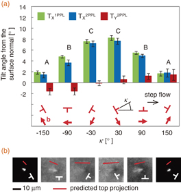
Fig. 3. (a) Tilt angles of six types of TED in 8° off-cut epilayers.  and
and  are the angles from the surface normal toward the step-flow
 ![$[11\bar{2}0]$](https://content.cld.iop.org/journals/1882-0786/7/12/121303/revision1/AP141071if007.gif) and
and ![$[\bar{1}100]$](https://content.cld.iop.org/journals/1882-0786/7/12/121303/revision1/AP141071if008.gif) directions, respectively, measured by 2PPL, and
directions, respectively, measured by 2PPL, and  is the angle toward the step-flow
 ![$[11\bar{2}0]$](https://content.cld.iop.org/journals/1882-0786/7/12/121303/revision1/AP141071if010.gif) direction measured using 1PPL side-view images. (b) Comparison between 1PPL plan views of TEDs and estimated top projection of TED lines.
direction measured using 1PPL side-view images. (b) Comparison between 1PPL plan views of TEDs and estimated top projection of TED lines.
Download figure:
Standard image High-resolution imageThe 1PPL plan-view imaging of TEDs exhibits six-type characteristic appearances depending on the direction of the extra half-plane, as shown in Fig. 3(b).13) Assuming straight dislocations, we can predict the top projection of a dislocation line for each type of TED from the epilayer thickness and the measured  and
and  values. The predicted projection lines (red line segments) are superimposed on the 1PPL TED images in Fig. 3(b). Effective correlation is confirmed in the lengths and tilt angles between the predicted lines and 1PPL images of the TEDs, revealing that the six-type characteristic appearances in 1PPL plan-view imaging are attributable to the tilts of TEDs toward different directions.
The pairs of  and
and  were converted to those of polar angles θ and φ in a crystal-base coordinate, where θ is the angle of the dislocation line from the c-axis and φ is the angle in counterclockwise between the projected dislocation line to the basal plane and the step-flow
 ![$[11\bar{2}0]$](https://content.cld.iop.org/journals/1882-0786/7/12/121303/revision1/AP141071if020.gif) direction.
direction.
The φ–θ plot of the TEDs is provided with error bars indicating confidence intervals (95%) in Fig. 4, where the "T" marks and b vectors are also included. The θ angles are distributed over 9–16° from the c-axis, and φ angles vary within the range of ±10°, showing that the dislocation lines are symmetrically projected on the basal plane with respect to the step-flow direction. Note that the "T" marks also exhibit the same symmetrical configuration, which means that the directions of the dislocation lines correlate with those of the extra half-plane.

Fig. 4. Plot of polar angles converted from  and
and  of TEDs in Fig. 3. θ is the angle from the c-axis for the dislocation line, and φ is the angle from the step-flow
 ![$[11\bar{2}0]$](https://content.cld.iop.org/journals/1882-0786/7/12/121303/revision1/AP141071if023.gif) direction in counterclockwise for the projected dislocation line to the basal plane.
direction in counterclockwise for the projected dislocation line to the basal plane.
Download figure:
Standard image High-resolution imageWe also conducted similar tilt-angle analysis for TSDs. As shown in Fig. 5, the frequency distributions (histograms) of TSD tilt angles are obtained for 40 TSDs in an 8° off-cut wafer (tepi = 140 µm) by 1PPL,12) (b) 39 TSDs in an 8° off-cut wafer (tepi = 26 µm) by 2PPL, and (c) 42 TSDs in a 4° off-cut wafer (tepi = 140 µm) by 2PPL. The tilt angles from the surface normal toward ![$[11\bar{2}0]$](https://content.cld.iop.org/journals/1882-0786/7/12/121303/revision1/AP141071if025.gif) are distributed from −2 to 9° for the 8° off-cut samples and from 1 to 10° for the 4° off-cut sample, indicating that the tilt angles of TSDs toward
are distributed from −2 to 9° for the 8° off-cut samples and from 1 to 10° for the 4° off-cut sample, indicating that the tilt angles of TSDs toward ![$[11\bar{2}0]$](https://content.cld.iop.org/journals/1882-0786/7/12/121303/revision1/AP141071if026.gif) are affected by the direction of the c-axis. Note that these angle distributions exhibit similar two-peak shapes.
are affected by the direction of the c-axis. Note that these angle distributions exhibit similar two-peak shapes.

Fig. 5. Histogram showing the distributions of tilt angles of TSDs from the surface normal toward the step-flow ![$[11\bar{2}0]$](https://content.cld.iop.org/journals/1882-0786/7/12/121303/revision1/AP141071if024.gif) direction. (a) 1PPL-measured angles for an 8° off-cut wafer, (b) 2PPL-measured angles for an 8° off-cut wafer, and (c) 2PPL-measured angles for a 4° off-cut wafer.
direction. (a) 1PPL-measured angles for an 8° off-cut wafer, (b) 2PPL-measured angles for an 8° off-cut wafer, and (c) 2PPL-measured angles for a 4° off-cut wafer.
Download figure:
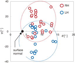
Standard image High-resolution imageFigure 6 shows the polar (φ–θ) plot provided by the 2PPL analysis for the 42 TSDs in the 4° off-cut sample (tepi = 140 µm). The θ angles vary over 5–15° from the c-axis, while the φ angles spread within ±40°. In this figure, "LH" and "RH" denote left- and right-handed TSDs, respectively, which have been determined by the appearance of each TSD in X-ray topography.25) The LH and RH regions clearly differ, parts of which overlap for the φ angle range of ±10°, while right- and left-handed TSDs tend to have positive and negative φ angles in the counterclockwise direction, respectively.
Fig. 6. Polar plot for 42 of TSDs in a 4° off-cut wafer (tepi = 140 µm). LH and RH denote left- and right-handed TSDs, respectively.
Download figure:
Standard image High-resolution image
A dislocation tends to be parallel, not only to the surface normal to minimize length, but also to the b vector because a pure screw dislocation has minimum elastic energy. The elasticity model explains that a dislocation line prefers to lie between the surface normal and the line parallel to the b vector. However, this simple model cannot explain the φ–θ plot for TEDs shown in Fig. 4. For example, the cases of κ = −90 and 90° yield negative (∼−6°) and positive (∼5°) φ values, respectively, although φ = 0 is expected from the elasticity model. We consider that the tilt angles of TEDs are governed not only by energetic stability in the bulk but also by kinetic interactions between advancing steps and the dislocations on a growing surface.
For the TSDs shown in Fig. 6, θ angles exceeding 5° are observed, and φ values vary within ±40°. For pure screw 1c dislocations, 0 < θ < 4° (off angle) and φ = 0 are expected from the elasticity model, although θ angles can be enhanced by the interactions of advancing off-steps.26) Recently, several groups have confirmed the existence of c + a dislocations in 4H-SiC crystals.3,27,28) For c + a dislocations, widespread θ values can be expected, and nonzero φ angles are possible depending on the directions of the a component vectors. The two-peak-shaped distributions of TX angles (Fig. 5) also support the existence of different types of TSD. The confirmation of the correlation between the line directions and Burgers vectors of TSDs (c or c + a dislocations) is a future subject. Moreover, the elasticity model cannot explain the difference between the LH and RH regions in the polar plot. This difference seems to originate from the interaction between surface spiral and advancing steps.
In conclusion, 2PPL band-edge emission enables the 3D imaging of TEDs, TSDs, and BPDs in 4H-SiC wafers for the first time in PL-based methods. The 3D imaging is possible to a depth of more than 200 µm from the epilayer surface. We measured the tilt angles of threading dislocations from the surface normal toward the ![$[11\bar{2}0]$](https://content.cld.iop.org/journals/1882-0786/7/12/121303/revision1/AP141071if027.gif) and
and ![$[\bar{1}100]$](https://content.cld.iop.org/journals/1882-0786/7/12/121303/revision1/AP141071if028.gif) directions and converted them to the polar angles θ and φ in a crystal-base coordinate. The polar angles of TEDs are found to correlate with the direction of the extra half-plane. For TSDs, the histograms of tilt angles toward the step-flow direction exhibit characteristic two-peak shapes. The φ–θ regions of left- and right-handed TSDs are found to differ, suggesting that the line directions of TSDs are affected by the interaction between the surface spiral and advancing steps. The 2PPL dislocation 3D-imaging technique provides a new methodology, which is also applicable to other semiconductor crystals, to investigate the propagation of dislocations during crystal growth.
directions and converted them to the polar angles θ and φ in a crystal-base coordinate. The polar angles of TEDs are found to correlate with the direction of the extra half-plane. For TSDs, the histograms of tilt angles toward the step-flow direction exhibit characteristic two-peak shapes. The φ–θ regions of left- and right-handed TSDs are found to differ, suggesting that the line directions of TSDs are affected by the interaction between the surface spiral and advancing steps. The 2PPL dislocation 3D-imaging technique provides a new methodology, which is also applicable to other semiconductor crystals, to investigate the propagation of dislocations during crystal growth.
Acknowledgments
This research was partly supported by the Japan Society for the Promotion of Science (JSPS) through its "Funding Program for World-Leading Innovative R&D on Science and Technology" (FIRST Program). We would like to thank Ms. Masako Ino of Nikon Corporation and Mr. Ken Shiya of Nikon Instech Co., Ltd. for operating the multiphoton microscopy system.