
Abstract
Two-step growth was employed to grow GaN quantum barriers (QBs) in InGaN green LD structures. A cap layer was grown at the same temperature as an InGaN quantum well (QW), and the temperature was then raised by around 130 °C to grow GaN QBs. The effects of low-temperature-grown cap (LT-cap) layers on the optical properties and microstructures of green LD structures were investigated. It was found that the LT-cap layer with an optimal thickness can improve the luminescence homogeneity and suppress the thermal decomposition of InGaN QWs. C-plane ridge waveguide laser diodes lasing above 500 nm were realized.
Export citation and abstract BibTeX RIS
InGaN green laser diodes (LDs) have attracted great attention over the past few years owing to their potential application in laser display. Several research groups have realized InGaN green LDs on either polar or semipolar GaN substrates.1–8) No matter which orientation is used, improving the crystalline quality of In-rich InGaN active layers is the key to realizing green LDs. However, growth details and microstructures of the InGaN active region in green LD structures have not yet been reported. The large difference in optimal growth temperature required for InGaN quantum wells (QWs) and GaN quantum barriers (QBs) is one of the difficulties in growing LD structures with high quality. To overcome this difficulty, two-step growth was employed to grow GaN QB layers in InGaN green LD structures in this work. We report the growth optimization of the InGaN/GaN active region with the aim to improve the luminescence homogeneity and suppress the thermal decomposition of InGaN QWs of green LD structures. Moreover, we report lasing above 500 nm, which is realized by the optimized growth of the InGaN/GaN active region.
Green LD structures were grown in a low-pressure metalorganic chemical vapor deposition (MOCVD) reactor. LD structures have the same layer structures except for the InGaN/GaN active region, consisting of a GaN/AlGaN:Si (2.5/2.5 nm) superlattice (SL) n-cladding layer, an InGaN:Si n-waveguiding layer, an InGaN/GaN MQW active region, an InGaN:Mg p-waveguiding layer, an AlGaN:Mg electron-blocking layer, a GaN/AlGaN:Mg (2.5/2.5 nm) SL p-cladding layer, and an InGaN:Mg p-contact layer. Conventional c-plane GaN/sapphire templates were used for growth optimization. Optimized green LD structures were then grown on free-standing GaN substrates, since smooth facets can be obtained by cleaving along the m-plane using free-standing GaN substrates. In order to obtain green emission, the growth temperature of InGaN QWs was set to be in the range from 690 to 700 °C. Our study showed that the crystalline quality of GaN layers grown in this temperature range was very poor, while it was much improved by increasing the growth temperature to 830 °C. Therefore, a two-temperature growth process for GaN QB layers was employed. A thin GaN cap (LT-cap) layer was grown at a rate of 0.016 nm/s at the same temperature as an InGaN QW without interruption, and then the temperature was raised by 130 °C at a ramped rate of 1.4 °C/s to grow another GaN barrier (HT-cap) layer. Our study showed that the LT-cap layer protects the InGaN QW layer during temperature ramping, and its crystalline quality is improved by the temperature ramping process. Therefore, it is expected that the thickness of this LT-cap layer will have a critical role because the protection of the InGaN QW layer will be inadequate if it is very thin, while its quality will be degraded if it is very thick. The growth optimization in this work was focused on the thickness of the LT-cap layer. Three groups of green LD structures with different nominal thicknesses of 1.2, 1.8, and 2.5 nm for the LT-cap layer were investigated, which are referred to as LD-12, LD-18, and LD-25 in the following. The optical properties of green LD structures were characterized by electroluminescence (EL) and micro-photoluminescence (micro-PL) measurements. Microstructures of InGaN active layers were investigated by high-angle annular dark field scanning transmission electron microscopy (HAADF-STEM).
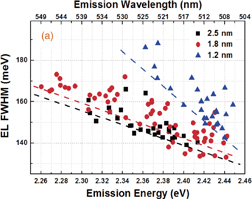
Pronounced broadening of spontaneous emission spectra is often observed for green LD structures owing to the reduced crystalline quality of the InGaN active region.9) Since maximum gain decreases significantly owing to inhomogeneous broadening, it is essential to suppress inhomogeneous broadening to realize green laser diodes and to improve their performance.10) EL full width at half maximum (FWHM) is an indication of the extent of inhomogeneous broadening and potential homogeneity in the active region. EL FWHMs of LD structures with different LT-cap layer thicknesses are plotted as a function of EL wavelength, as shown in Fig. 1(a). Each data point represents an LD structure, while the dashed lines plotted along the lower limit of the EL FWHMs are guides for the eyes. Each data point also shows that the EL FWHM of each group of samples tends to increase with emission wavelength, which is an indication of enhanced potential inhomogeneity as the indium composition in the InGaN QWs increases.9) However, note that the EL FWHM of LD-12 is larger than those of LD-18 and LD-25, which show a more pronounced increase with increasing wavelength. As mentioned previously, the LT-cap layers protect the InGaN QW layers from decomposition during temperature ramping. Therefore, we believe that the LT-cap layers with a nominal thickness of 1.2 nm in LD-12 may not be thick enough to protect the InGaN QW layers, which induces additional fluctuations of InGaN QW layer thickness and indium composition caused by indium desorption. It is considered that this effect increases as the indium composition of the InGaN QW layers further increases. As a result, the EL FWHM of LD-12 markedly increases with wavelength. On the other hand, the guide lines for the EL FWHM lower limits of LD-18 and LD-25 have similar slopes, which suggests that LT-cap layers with nominal thicknesses of 1.8 nm and higher can fully protect the InGaN QW layers from temperature ramping.
Download figure:
Standard image High-resolution image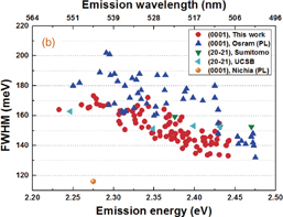
Fig. 1. (a) Wavelength-dependent FWHMs of green LD structures with various LT-cap layer thicknesses. The dashed lines are guides to the eyes. (b) Shows the FWHMs of green LD structures from this and other works. Note that the measured conditions are different for data from different groups. The current density of our measurements is 10 A/cm2 under the DC condition, while it is reported to be 14 A/cm2 for semipolar green LEDs by UCSB11,12) and 150 A/cm2 for semipolar green LD structures by Sumitomo Electric Industries.13) PL data are used for c-plane green LD structures manufactured by Osram14) and Nichia.15)
Download figure:
Standard image High-resolution imageAs shown in Fig. 1(b), we compare the EL FWHMs of our optimized LD structures with the FWHMs reported in other works. Note that the measured conditions are different for data from different groups since only limited data are available in the literature. The current density of our measurements is 10 A/cm2 under the DC condition, while it is reported to be 14 A/cm2 for semipolar green LEDs by UCSB11,12) and 150 A/cm2 for semipolar green LD structures by Sumitomo Electric Industries.13) PL data are used for c-plane green LD structures manufactured by Osram14) and Nichia.15) These data show that our FWHM for an emission wavelength of 530 nm (2.34 eV) is roughly comparable to those from the other works except for that recently reported by Kyoto University and Nichia for a c-plane green LD structure,15) which is remarkably narrower than those from all other works, although it is a PL FWHM for undoped LD structures. This result indicates that the potential inhomogeneity of Nichia's LD structure is significantly suppressed. We believe that the capping technique used in our LD structures suppresses the potential inhomogeneity more related to well thickness fluctuation. However, the potential inhomogeneity caused by In composition fluctuation must be further reduced. In composition fluctuation may be more related to InGaN QW growth conditions such as growth rate and temperature.
In order to study the effect of LT-cap layer thickness on the microstructures of the InGaN/GaN active region, HAADF-STEM measurements were carried out. The STEM images of InGaN/GaN active layers with LT-cap layer thicknesses of 2.5 and 1.2 nm are shown in Fig. 2. For InGaN QW layers covered by a 2.5 nm LT-cap layer prior to temperature ramping, continuous InGaN QWs are observed, as shown in Figs. 2(a) and 2(c). The thickness of the InGaN QWs is determined to be 2.5 nm. As shown in Figs. 2(b) and 2(d), for the LD structure with an LT-cap layer thickness of 1.2 nm, InGaN QWs turn out to be broken, and separated InGaN islands can be observed clearly. The height of these InGaN islands is about 2.5 nm, the same as the intended thickness of InGaN QW layers. This result indicates that the 1.2-nm-thick LT-cap layer is insufficient for protecting InGaN QWs from temperature ramping. These island structures may form when the temperature is ramped from 700 to 830 °C and growth is interrupted owing to the absence of triethylgallium (TEGa) or trimethylindium (TMIn) in the chamber. During this stage, LT-cap layers may locally decompose owing to thermal annealing. For the LD structures with 1.2 nm LT-cap layers, the decomposition of LT-cap layers may have exposed InGaN QWs partially, resulting in the desorption of indium from InGaN QWs and the fluctuation of InGaN QW thickness. In contrast, for the LD structures with 2.5 nm LT-cap layers, the LT-cap layers were thick enough to protect the InGaN QWs from temperature ramping, forming homogeneous InGaN QWs. Composition analysis indicates that the indium composition is highest at the center of the islands and decreases towards the peripheral regions. As a result, EL emission broadens owing to fluctuations of both InGaN layer thickness and indium composition.

Fig. 2. STEM images of InGaN/GaN active region of green LD structures with various LT-cap layer thicknesses: (a) 2.5 and (b) 1.2 nm LT-cap layers. (c) and (d) are magnifications of the circled areas in (a) and (b), respectively.
Download figure:
Standard image High-resolution imageThe thermal degradation of the InGaN/GaN active region is another main obstacle in realizing green LDs. A GaN:Mg/AlGaN:Mg p-cladding layer with a thickness of around 500 nm or larger must be grown for an LD structure, and the growth temperature of this p-cladding layer cannot be lowered too much to maintain sufficient electrical conductivity. Therefore, the thermal budget, which is proportional to the growth temperature and duration of the p-cladding layer, in the InGaN/GaN active region is much higher than that in LED structures. Thermal degradation has been observed in both polar and semipolar green LD structures.16–18) We have reported the microstructures of degraded InGaN/GaN active regions where the thermal decomposition of InGaN QWs occurs and metallic indium forms.16) The degraded regions appear as dark spots in micro-PL images owing to nonradiative recombination. Actually, we observe a correlation between the LT-cap layer thickness and the appearance of dark spot defects in green LD structures. The micro-PL images of LD structures with 1.2-, 1.8-, and 2.5-nm-thick LT-cap layers are shown in Fig. 3. It can be seen that dark spots appear only in the LD structure with the 2.5-nm-thick LT-cap layer. We believe that both the thermal budget and crystalline quality of the InGaN/GaN active region are critical factors impacting the InGaN decomposition. Here, the thermal budget is the driving force, while defects within or surrounding InGaN QWs are diffusion paths for the formation of metallic indium precipitates. The appearance of dark spots only in the LD structure with the 2.5-nm-thick LT-cap layer indicates that there are more defects in the 2.5-nm-thick LT-cap layer, which facilitate the diffusion and aggregation of indium atoms, and therefore results in the formation of metallic indium precipitates.

Fig. 3. Micro-PL images of green LD structures with various nominal LT-cap layer thicknesses of (a) 1.2, (b) 1.8, and (c) 2.5 nm.
Download figure:
Standard image High-resolution imageIt is reasonable to assume that more defects exist in the 2.5-nm-thick LT-cap layer because although the temperature ramping following the LT-cap layer growth improves the crystalline quality, its impact decreases as the LT-cap layer thickness increases. In order to study this aspect, three single InGaN QW samples covered by an LT-cap layer and then an HT-cap layer were grown. The LT-cap layer thicknesses are 1.2, 1.8, and 2.5 nm, while the HT-cap layer thickness is 8 nm. Figure 4 shows the PL spectra of these samples. It can be seen that the InGaN QW samples with the 1.2 and 1.8 nm LT-cap layers have almost the same PL intensity, while the InGaN QW sample with the 2.5 nm LT-cap layer has a much lower PL intensity. We believe that thermal annealing is not adequate for the 2.5-nm-thick LT-cap layer. Therefore, there are more defects in the LT-cap layer, which result in a higher nonradiative recombination.

Fig. 4. PL spectra of single InGaN QW samples with various LT-cap layer thicknesses.
Download figure:
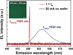
Standard image High-resolution imageAfter the luminescence homogeneity of green LD structures was improved and the thermal degradation was eliminated, a green LD structure was then grown on a bulk GaN substrate and fabricated into ridge waveguide LD chips. Micro-PL measurements of the LD structure indicate the absence of dark spots, as shown in the inset of Fig. 5. The spontaneous emission peak and lasing wavelengths of the LD structure are 532 and 503 nm, respectively. The threshold current at room temperature is 400 mA under pulse operation with a 300 ns pulse width and a 10 kHz repetition frequency for the LD chips with a ridge width of 4 µm and a cavity length of 400 µm, and the threshold current density is 25 kA/cm2, which is relatively high partially owing to the small cavity length. Note that the blue shift from spontaneous emission to lasing is as large as 29 nm, which may be attributed to the high threshold current density.
Fig. 5. EL spectra of green LD below and above threshold current. The inset shows the micro-PL image of the green LD structure.
Download figure:
Standard image High-resolution image
In summary, two-step growth with a thin LT-cap layer followed by an HT-cap layer was employed to grow GaN QB layers in green InGaN LD structures. Our results show that the LT-cap layer with an optimal thickness can improve the luminescence homogeneity and suppress the thermal decomposition of the InGaN active layer. C-plane ridge waveguide laser diodes lasing above 500 nm were realized.
Acknowledgments
This work is supported by the Natural Science Foundation of China (Grant Nos. 61334005 and 61076119), the National High Technology Research and Development Program of China (863 Program) (Grant Nos. 2013AA030502 and 2013AA031901), the Science and Technology Support Project of Jiangsu Province (Grant No. BE2013007), and the Strategic Priority Research Program of the Chinese Academy of Sciences (Grant No. XDA09020401).