


Abstract
Ferromagnetic shape memory alloys are characterized by strong magneto-mechanical coupling occurring at the atomic scale causing large magnetically inducible strains at the macroscopic level. Employing combined atomic and magnetic force microscopy studies at variable temperature, we systematically explore the relation between the magnetic domain pattern and the underlying structure for as-deposited and freestanding single-crystalline Fe7Pd3 thin films across the martensite–austenite transition. We find experimental evidence that magnetic domain appearance is strongly affected by the presence and absence of nanotwinning. While the martensite–austenite transition upon temperature variation of as-deposited films is clearly reflected in topography by the presence and absence of a characteristic surface corrugation pattern, the magnetic domain pattern is hardly affected. These findings are discussed considering the impact of significant thermal stresses arising in the austenite phase. Freestanding martensitic films reveal a hierarchical structure of micro- and nanotwinning. The associated domain organization appears more complex, since the dominance of magnetic energy contributors alters within this length scale regime.
Export citation and abstract BibTeX RIS

Content from this work may be used under the terms of the Creative Commons Attribution-NonCommercial-ShareAlike 3.0 licence. Any further distribution of this work must maintain attribution to the author(s) and the title of the work, journal citation and DOI.
Changes were made to this article on 24 July 2013. Reference links were corrected.
1. Introduction
Ferromagnetic shape memory alloys constitute a highly promising class of materials for miniaturized actuation and sensing applications. Besides Ni–Mn–Ga, where the ferromagnetic shape memory effect was first discovered [1], Fe–Pd-based alloys with compositions close to Fe7Pd3 [2] have more recently attracted significant interest for complementary applications, where low brittleness, high ductility [3] and biocompatibility [4] are required. Concerning the latter property, it is a highly promising candidate for actuators and sensors in biomedical environments.
Based on magnetically induced reorientation of martensite variants, a single crystal of the correct disordered face-centered tetragonal (fct) martensite phase constitutes an essential prerequisite for magnetic actuation, as it reveals sufficiently high twin boundary mobility and pronounced magnetocrystalline anisotropy [3], with the easy axes aligned to the longer a-axes. Since fully operational fct martensite is characterized by strong magneto-elastic coupling, which in turn enables twin boundary motion in an external magnetic field, the interplay of structure and magnetic configuration especially at small scales as well as perturbations due to constraints such as stresses are of particular interest. A combined study based on atomic force microscopy (AFM) as well as magnetic force microscopy (MFM) observations can thus be expected to be suitable to gain a deeper understanding.
So far, MFM measurements have only been performed on polycrystalline Fe7Pd3 ferromagnetic shape memory alloys [5, 6] and on polycrystalline L10-type Fe5Pd5 [7, 8], which has attracted increased interest in the field of perpendicular magnetic recording, but does not show the magnetic shape memory effect. This work focuses on single-crystalline fct martensitic Fe7Pd3 thin films that are a precondition for miniaturized magnetic actuators and allow for novel insights due to the coupling of structure and magnetism, as we demonstrate in this study.
2. Experimental details
Single-crystalline Fe7Pd3 thin films were grown on MgO (001) single crystals by molecular beam epitaxy from two independent rate-controlled electron beam evaporators with a total deposition rate of approximately 0.15 nm s−1 and a substrate temperature of 900 °C at ultra-high vacuum conditions (base pressure lower than 10−9 mbar)—as described in detail before [9]. Upon cooling, these films traverse the austenite–martensite transition slightly above room temperature (deviations of a few kelvins may appear due to off-stoichiometry and stresses) [10]. Several films were subsequently released by dissolving the MgO substrate using sodium bicarbonate, as proposed earlier [11]. Prior to AFM/MFM investigations, samples were routinely characterized with respect to their phase appearance at room temperature by means of x-ray diffraction (XRD) using CuKα radiation in Θ/2Θ geometry. For twinned martensite samples, phase identification was complementarily performed in real space by the unique degree of tetragonality, based on the c/a ratio of the short c- and long a-axis. Ratio determination was taken from surface reliefs obtained using AFM (figure 1). This was done by averaging over ten independent profiles and employing the relation  [12].
[12].

Figure 1. (a) Scheme of a martensitic sample consisting of a twinned two-variant configuration. (b) Detailed sketch of the twinning planes. The surface corrugation angle α is related to the c/a ratio of a unit cell. The phase can thus be determined via AFM surface relief analysis.
Download figure:
Standard image High-resolution imageThe specimens used for experiments in this paper consist of 28.2–29.8 at.% Pd. Their average thickness amounts to 500 nm. Due to a distinct island growth with deep descents—correlated to high deposition temperatures—the thickness at smooth plateaus of sample M1 amounts to 640–670 nm. Martensitic (M) specimens M1–M3 exhibit the martensitic phase and were examined as-deposited, while the freestanding martensitic samples are denoted FS1 and FS2. The austenitic sample (A) was partially lifted off to investigate the influence of substrate constraints as discussed later. All phase appearances mentioned here refer to room temperature.
To obtain information on the interior structure, scanning electron microscopy (SEM) images were acquired from specimen cross sections prepared using a focused ion beam (FIB)4. Combined AFM/MFM experiments were performed with commercial systems5. An oscillating tip with a magnetic Cr/Co coating6 first scans the sample surface in intermediate (AC/tapping) mode to acquire topography and subsequently returns in lift mode with an offset to the surface profile of typically several tens of nanometers. The phase shift between excitation- and cantilever frequency is recorded, yielding magnetic information. The tip was magnetized parallel to the oscillation direction, i.e. normal to the sample surface, and is consequently sensitive to the normal magnetic stray field component Hz. The characteristic twinning periods and domain stripe widths are determined by employing the azimuthally averaged autocorrelation function C(R) [13] of height map z (x,y) and magnetic image φ (x,y), respectively.
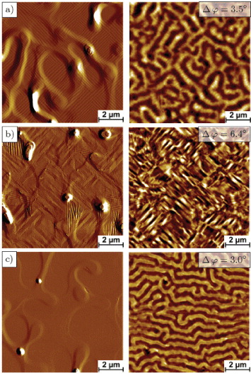
Figure 2. Amplitude error images of topography (left) and MFM phase contrast maps (right) of (a) as-deposited sample M1. The color-coded MFM contrast reveals magnetic stripe domains that are predominantly aligned normal to the martensite twin boundaries, which are visible due to the corresponding regular surface corrugation pattern. (b) Specimen M2 with topography predominantly free of the regular surface corrugation pattern, but a weaker stripe morphology. In this sample in-plane twinning occurs. Magnetic domains, located within these twin variants, show a more pronounced magnetic contrast than in regions with a regular twinned surface such as specimen M1. (c) As-deposited austenitic sample A. The magnetic domain patterns are very similar to the martensitic sample. Due to lower film corrugations, magnetic domains with one preferential orientation can be observed.
Download figure:
Standard image High-resolution image3. Experimental results
3.1. As-deposited films at room temperature
As illustrated in figure 2(a), a surface corrugation pattern correlated to nanotwinning is readily resolved for sample M1. An exemplary XRD spectrum to confirm the fct phase of sample M1 is presented in figure 3. AFM measurements reveal c/a ≈ 0.92 ± 0.03, which additionally corroborates the presence of the fct phase.
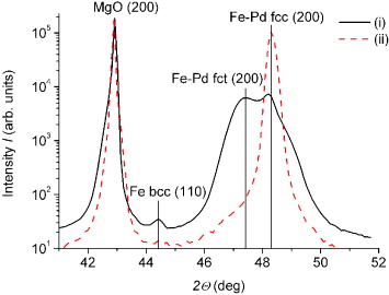
Figure 3. XRD measurements of epitaxially grown single-crystalline Fe7Pd3 thin films on MgO: (i) at the martensite–austenite phase transition with fcc austenite and different martensite variants (sample M1); (ii) a prevalent austenite film (sample A). The Fe bcc (110) peak originates from iron precipitations between substrate and Fe7Pd3 thin film, as discussed before [9].
Download figure:
Standard image High-resolution imageAn area of 10 × 10 μm2 was investigated using MFM and AFM. Instead of topographies, the amplitude error images are shown in figure 2, since they yield a better contrast especially for weak features such as a twin variant corrugation pattern. As for sample M1, bright and dark magnetic domain stripes can be observed, indicating moments that point in opposite directions (see figure 2(a)). Correlations between magnetic domains and martensite structure are readily identified: while smooth plateaus exhibit stripe domains oriented normal to the twin variant pattern, angular deviations are observed at steep descents. The domain stripe width amounts to λ = 400 ± 30 nm. The average twin variant width is found to be 95 ± 15 nm.
In figure 2(b), combined AFM/MFM measurements of sample M2 can be seen. They exhibit microscopic regions, where the regular surface corrugation pattern is absent. Instead, a much weaker surface corrugation with a twice greater periodicity is present. The MFM micrograph reveals magnetic domains located only within these stripe areas separated by the corrugation lines. Moreover, the phase shift between these domains is more pronounced than in regular corrugated areas, indicating a larger out-of-plane magnetization. A closer insight into structural features occurring beneath the surface is given in the cross-sectional SEM images depicted in figure 4. While regions with the regular twinned surface corrugation pattern reveal a 45° angle between twin boundary orientation and the film normal (in accordance with the scheme in figure 1(a)), areas exhibiting weak corrugation stripes are characterized by variant twinning in the surface plane, meaning that crystal orientation is rotated by 90° with respect to the usual structure and one of the two easy a-axes is always aligned normal to the surface plane.

Figure 4. Cross-sectional SEM images of sample M2 cut with FIB parallel to the substrate edge and to the (100)A plane respectively, in different sample regions. (a) The typical corrugation pattern is characterized by twin boundaries aligned parallel to the MgO substrate edges and under 45° to the substrate surface (parallel to the (101)A plane). (b) The twin boundaries in the weak corrugated areas of M2 align under 45° to the MgO substrate edges and normal to the surface plane (parallel to the (110)A plane). For better visualization, the contrast of the SEM images was increased.
Download figure:
Standard image High-resolution imageAlthough martensitic samples are of central relevance for magnetically induced actuation or sensing, it is, however, instructive to address micromagnetic characteristics of the parental austenitic phase (see figure 2(c)). It is surprising, at first glance, that a well-ordered domain stripe pattern with significant out-of-plane magnetization and λ = 360 ± 10 nm can be observed, which will be discussed in section 4.
3.2. Freestanding films at room temperature
By applying a lift-off approach as suggested earlier [10, 11], structurally intact freestanding films are prepared. As visible in the topography signal of figure 5, a hierarchical martensite structure occurs. It is dominated by a micrometer-sized stripe variant pattern of 1400–2000 nm periodicity. Elevated microvariants (EM) show no morphological subfeatures at the surface but the FIB cut (not shown here) reveals twin boundaries oriented normal to the substrate plane in some areas. In contrast, lower microvariants (LM) yield regions of regular nanotwinning. A well-pronounced magnetic domain stripe pattern can be seen in EM, whereas almost no out-of-plane magnetization is observed in LM. Only within nanotwinned regions, a weak magnetic domain stripe contrast forms. Taking a closer look at the connection between different microvariants (figure 5(c)), those of EM coincide with the domain walls in LM.

Figure 5. (a) Amplitude error image of topography (left) and MFM phase contrast map (right) of the freestanding specimen FS1. The amplitude error image reveals a line-shaped hierarchical twin structure. Lower microvariants (LM)—containing nanotwins and exhibiting poor out-of-plane magnetization—alternate with elevated untwinned microvariants (EM) yielding strong Mz component. (b) Height profile along the line marked in the amplitude error image and in the MFM phase contrast map; scheme of hierarchical variant morphology with only partially twinned microvariants. (c) Magnified view highlighting coinciding magnetic domain walls of neighboring microvariants (circle).
Download figure:
Standard image High-resolution imageSimilar micromagnetic characteristics can be obtained at the sample's back side (formerly attached to the substrate) as depicted in figure 6. The topography furthermore contains a residual island pattern originating from early stage growth mechanisms at elevated temperatures [14]. A microvariant superstructure—similar to that of the front side—is, however, absent.

Figure 6. Height (left) and MFM phase (right) image of the substrate side of specimen FS2. No stripe-shaped microvariant structure can be observed anymore, but the height difference between twinned and untwinned areas as well as between regions with low and high magnetic contrast is much more pronounced.
Download figure:
Standard image High-resolution imageReferring back to specimen A, appearing in the austenite phase at room temperature, we performed a partial lift-off to examine its domain structure in detail. It turns out that as-deposited regions remain unchanged, but the magnetic domain pattern illustrated in figure 2(c) is absent in freestanding regions (not shown here).
3.3. Structure and micromagnetism across the martensite–austenite transformation
Temperature-dependent AFM/MFM measurements across the austenite–martensite transition on as-deposited sample M3 and lift-off specimen FS1 are described in the following.
Figures 7(a)–(f) show the results for M3 at five temperatures between 293 and 370 K. At room temperature, the regular surface corrugation structure (AFM) and corresponding stripe domain pattern (MFM) can be observed again.

Figure 7. Amplitude error images of topography (left) and MFM phase contrast maps (right) of as-deposited sample M3 measured at five different temperatures between 293 and 370 K and after cooling down to room temperature.
Download figure:
Standard image High-resolution imageA gradual austenite transition already occurs at 325 K (figure 7(b)) where a major fraction of the twin variant corrugation pattern disappears and the maximum MFM contrast Δφ drops slightly. At 370 K the surface is free from any features related to variant twinning and the austenite phase established completely. The contrast of the magnetic stripe domain pattern steadily decreases with higher temperatures, but does not disappear even at 370 K. During the heating process, some minor regions exhibit domain stripe alignment tendencies. The structural phase transition extends over a temperature range of a few tens of kelvins. Noteworthy is the fact that the domain stripe width λ remains unaffected. Comparing the initial surface morphology with the one at room temperature after a heating cycle, minor changes concerning the twin orientation can be seen. A domain reconfiguration to its initial state could not be observed during cooling.
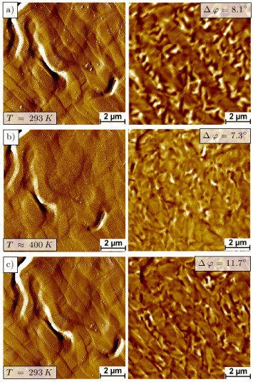
Analogous investigations on the freestanding specimen FS1 (figures 8(a)–(c)) reveal different behavior. During the heating process, a minor fraction of nanotwins vanished. It could, however, not be verified whether the film traverses a phase change locally or whether vanishing of surface corrugation is only artificial due to thermally induced noise by the sample heater. At higher temperatures, the magnetic contrast in EM decreases and the magnetic domain pattern gets blurry and the domains are not strictly limited to one type of microvariant anymore. Due to limited heating power of the Peltier element used, only temperatures up to 400 K could be achieved. On cooling down to room temperature, the magnetic contrast in EM increases again.
Figure 8. Amplitude error images of topography (left) and MFM phase contrast maps (right) of sample FS1 measured at room temperature and T ≈ 400 K as well as after cooling back down to room temperature. The given temperatures refer to the Peltier element.
Download figure:
Standard image High-resolution image
4. Discussion
4.1. As-deposited and freestanding thin films at room temperature
The experimental results given in the previous section can be summarized as follows. (i) A magnetic stripe domain pattern with detectable out-of plane magnetization occurs in regularly twinned martensite Fe–Pd thin films and is aligned predominantly perpendicular to the twin corrugation pattern. (ii) In several martensitic samples—as exemplarily shown on M2—regions without this regular corrugation pattern also occur. They contain an in-plane twinning with larger variant width and the corresponding magnetic domain pattern is characterized by stronger z magnetization Mz. These domains are furthermore confined within variants rather than forming a pattern similar to regular twinned areas. (iii) As-deposited austenite reveals a distinct out-of-plane magnetic domain stripe pattern, which vanishes after lift-off. (iv) A hierarchical stripe morphology emerges in freestanding martensite films. It is characterized by varying EM and LM, where the latter partially contain a corrugation pattern due to regular twinning. Despite the fact that EM do not yield any similar surface features detectable by AFM, cross-sectional SEM micrographs reveal the partial presence of in-plane variant twinning as schematically drawn in figure 5(b). Magnetic domains with strong out-of-plane components can be readily resolved in EM, whereby domain walls are mainly visible in LM.
In general, the occurrence of magnetic domains in ferromagnets originates from the long-range dipole–dipole interaction occurring between atomic magnetic moments. By introducing such domains of different magnetic orientation, a loop closure of magnetic flux lines is achieved and stray fields effectively reduce. The overall magnetostatic energy—correlated to this interaction—can in turn be minimized at the macroscopic level. As a consequence, this contributor to the overall magnetic energy of a ferromagnet forces magnetic moments into the surface plane if they are located close to open boundaries. The long-range character of the underlying magnetic dipole interaction makes it moreover sensitive to a specimen's geometry ('shape anisotropy energy'). This energy term therefore heavily impacts on domain characteristics in systems such as thin films, where the surface-to-volume ratio attains extremal values. As already frequently observed, a domain stripe pattern with altering in-plane magnetization often occurs in such films. This highly ordered configuration further reduces stray fields appearing at the film sides.
Once significant (but not too high) uniaxial magnetocrystalline anisotropy arises in the surface plane, the domain stripe pattern aligns along the easy axis. If the easy axis is oriented normal to the surface, magnetization slightly rotates out-of-plane and is detectable by MFM. Once the amount of this magnetocrystalline anisotropy increases, not only moment Mz components and domain stripe widths/wall widths are affected [15] but also the order of the stripe pattern may transform to a maze structure or even toward unordered island-like domain configurations in the case of a dominating magnetocrystalline energy contribution [16]. This explanation leads to the discussion of finding (i). A nanostructural influence in the form of regular twinning—as a predominant structural feature in as-deposited thin films—causes an angular alternation of one easy a-axis. Variants having both easy axes in-plane clearly prefer moments to lie in-plane as well since this state is additionally supported by the strong magnetostatic energy fraction. Neighboring variants with one a-axis normal to the film surface, however, allow for a significant Mz component. The low lateral variant extension of about 100 nm additionally promotes magnetic coupling [17]. The occurrence of variant twinning at small scales may therefore be associated with a reduced average out-of-plane magnetocrystalline easy axis causing an ordered stripe pattern with lower out-of-plane magnetization. This is in accordance with comparable low MFM phase shifts compared to those observed in microvariants of lift-off films (see figure 2(a) versus figure 5(a)) as well as irregular twinned areas (figure 2(a) versus figure 2(b)).
This leads us to the consideration of finding (ii). As mentioned before, smooth areas with a weak irregular surface corrugation pattern are characterized by in-plane twinning (twin boundaries parallel to the (100) and (010) planes, respectively). A similar irregular corrugation pattern has been reported for Ni–Mn–Ga, and an explanation was given in terms of tilted modulated variants [18, 19]. The origin in Fe–Pd has not been discovered yet but intrinsic stresses as well as a phase reconfiguration close to the substrate interface are reasonable causes.
However, the occurrence of variant twinning within a surface plane is connected to a shift in energetic balance with respect to the regular type addressed in (i). The magnetocrystalline influence benefits from the fact that one easy a-axis permanently aligns to the surface normal and the angular alternation of the magnetically hard c-axis within the surface partially weakens the influence of shape anisotropy. Moreover, variant widths are approximately twice as large as in regular twinned regions, leading to a less pronounced magnetic coupling via stray fields. As a consequence, magnetic domain extension is predominantly limited within a variant type and yields significantly stronger Mz components causing higher MFM phase shifts.
As mentioned in finding (iii), an austenite specimen should exhibit cubic magnetocrystalline anisotropy. Indeed, Cui et al reported on magnetocrystalline anisotropy with the easy axes aligned to the 〈111〉 directions for single-crystalline austenite bulk Fe7Pd3. However, this anisotropy constant amounts to Kcubic = (− 5 ± 2) × 102 J m−3 [3] and is two orders of magnitude lower compared to the uniaxial counterpart measured in the martensite phase. Obviously, the magnitude of Kcubic as well as the symmetry of cubic magnetocrystalline anisotropy are not sufficient to face the magnetostatic anisotropy term.
We demonstrated that films grow virtually stress free during deposition at high temperatures [9]. Major stresses arise during sample cooling due to different thermal expansions of both substrate and thin film. Many studies examined the invar properties of Fe7Pd3 [10, 20, 21], and Matsui et al determined the linear thermal expansion coefficient as αFe−Pd ≈ 9 × 10⁻⁶ K−1 for Fe68Pd32 at room temperature. Considering a value of αMgO = 10.8 × 10⁻⁶ K−1 for the MgO substrate [22], this results in a biaxial compressive stress acting on Fe7Pd3 during cooling [10]. Due to volume conservation, the austenite fcc cell should be tetragonally distorted and the unit cell vector normal to the film plane slightly extends. Since Fe7Pd3 prefers a long axis to be the magnetically easy one, a stripe domain pattern with detectable Mz may occur once the thermally induced uniaxial Kstress is large enough. The disappearance of magnetic domains in lifted austenitic films confirms the suggestion of a stress-induced magnetocrystalline anisotropy as a reasonable origin.
According to Kittel's theory [15], a modified model system of partial flux closure [17] was utilized to estimate Kstress in our austenite Fe7Pd3 thin film A. The total magnetic energy per unit area—consisting of the sum of magnetostatic energy, stress-induced anisotropy energy and a wall energy—is therefore calculated analytically. Material-specific exchange constant A (≈ 2 × 10⁻¹¹ J m−1), saturation magnetization Ms and film thickness t have to be considered as well. The total energy is minimized with respect to the domain width and to a parameter η, which determines the amount of flux closure [17]. In the case of the austenite specimen A with a domain width of λ = 360 nm, we estimate a stress-induced uniaxial second-order anisotropy constant of Kstress ≈ (3.8 ± 0.4) × 104 J m−3 that is basically sufficient to explain the presence of the domain stripe pattern observed by MFM.
The formation of a hierarchical variant pattern and correlated magnetic features as addressed in finding (iv) and illustrated in figures 5(a) and 6 is clarified in the following. As is generally known, the introduction of lattice misfit dislocations at substrate interfaces is the preferred mechanism to reduce film stresses beyond a critical thickness of several nanometers. In the case of epitaxially grown Fe–Pd films presented here, such dislocations can also be found as stated in [9]. After film lift-off, some of these defects relax toward the surface, but others remain within the film. As pinning centers, they affect the phase transitions probably occurring after lift-off as well as the formation of hierarchical structures as a mechanism of stress relaxation [11]. Further intrinsic stresses may arise due to the formation of Fe precipitates. They can be observed at the film's substrate side and occur during the deposition to minimize lattice misfits [9]. Iron precipitates may therefore be a reason for a more distinct roughness at the sample back side and the absence of an ordered microvariant surface morphology (see figure 6). In general, a hierarchical twin structure indicates the compensation of shear stress fields arising in the specimen [23]. Currently, transmission electron microscopy measurements are in progress to investigate in more detail which mechanism is the major origin.
However, EM—characterized by a strong magnetic contrast—can be treated like those discussed in point (ii), where one long magnetically easy a-axis permanently points normal to the film plane. Crystal orientation in LM is rotated by 90° with respect to that observed in EM. Both easy axes are aligned in the surface plane, resulting in poor MFM contrast. Only in subregions of regular twinning—partially occurring therein—the formation of a weak stripe domain pattern can be observed again. The distinct height difference between both microvariant types originates from the tetragonality of martensite unit cells. The coincidence of domain walls at neighboring microvariants implies an interplay between their demagnetization fields.
4.2. Temperature-dependent MFM
In as-deposited martensite films M1 and M2, the twin structure completely recovers after a heating–cooling cycle across the structural transition with only minor changes. These changes can be explained considering dislocations (e.g. Fe precipitates, etc) located at the substrate side of the thin film. During thermally induced structural phase transitions, local relaxation processes due to generation and relaxation of biaxial in-plane stresses are most probably correlated to a change in defect configuration. The surface roughness of the substrate and associated local stress gradients may also generate varying twin nucleation seeds. Furthermore, the temperature interval of the phase transition of a few tens of kelvins can be at least partially attributed to stress gradients correlated to substrate constraints, defects and roughness.
As we know from a comparison of freestanding and as-deposited austenitic films, the formation of magnetic domains can be traced back to magnetocrystalline anisotropy due to thermal stresses. Considering the thermally induced austenite transition, an interesting point is the fact that only minor changes in the magnetic stripe domain pattern occur. These minor alignment tendencies are probably connected to local stress relaxations during heating. After cooling across the martensite transition, the slightly modified domain configuration remains, which is probably due to the non-elastic nature of local stress relaxations. Furthermore, a wider hysteresis—associated with this first-order phase transition—may have an additional influence. Further cooling would thus be necessary to obtain a (partial) recovery. However, in the case of as-deposited twinned Ni–Mn–Ga thin films, a well-pronounced drop in MFM phase contrast as well as a significant change in domain stripe width are reported at the phase transition [17]. The comparably low MFM phase drop and the absence of a similar domain width reduction in our Fe–Pd films might be associated with a simultaneous change of several competing material properties. For instance, the effectively reduced average easy axis normal to the surface plane—associated with regular twinned fct martensite (one easy a-axis alternates directions and the other easy axis always lies in-plane as addressed in finding (i))—could be close to the estimated value of stress-induced uniaxial anisotropy in as-deposited austenite. Moreover, the saturation magnetization in austenite of Ms,fcc ≈ 0.89Ms,fct [3] leads to a lower influence of the shape anisotropy energy contribution in the parental phase and promotes a more pronounced Mz component of the domain stripe pattern. These assumptions are strengthened by temperature-dependent MFM measurements on freestanding films. Magnetic domains become blurred and less pronounced in the MFM phase shift, as it would be expected for transition to a magnetocrystalline cubic phase.
It is, however, questionable whether the microvariant structure and domain pattern would vanish completely at even higher temperatures. On the one hand, observed microvariant superstructures do not yield a twin structure in the common sense, but a plateau-like topography as schematically shown in figure 5(b). It is not yet clear whether the hierarchical structure is completely decoupled from typical martensitic twinning. On the other hand, the existence of lattice dislocations at the film back side could be the cause for a partial austenite transition during heating. They may induce the hierarchical structure by pinning and hinder the phase transition as well. Furthermore, a change in crystalline structure, due to the lift-off process, might be a reason for this phenomenon. Measuring the c/a ratio of the surface corrugation pattern, partially occurring in LM (see figure 5(a)), does not only yield a clear identification of fct structure but also between fct and bct martensite. The latter is thermally stable [3, 24] and could hinder the complete martensite–austenite transition.
5. Conclusions
Temperature-dependent AFM and MFM measurements were performed across the structural phase transition of as-deposited and lift-off Fe7Pd3 thin films appearing in the fct martensite and austenite phases at room temperature, respectively. This non-destructive tool allowed a qualitative explanation of the correlation between crystallographic features and the corresponding magnetic domain pattern in as-deposited fct martensite thin films.
Fcc austenite films also reveal a pronounced magnetic domain stripe pattern as long as they are still attached to the substrate. We attribute this finding to bi-axial in-plane stresses due to the low linear thermal expansion coefficient of Fe7Pd3, which is known for its invar anomalies [20]. A stress-induced uniaxial anisotropy Kstress—correlated to a tetragonally distorted austenite unit cell with a long easy out-of-plane axis—is estimated utilizing an analytical model of partial flux closure.
AFM measurements on freestanding martensite films reveal the disappearance of a major fraction of nanotwinned variants, which is correlated to the absence of thermal stresses after lift-off. A minor fraction of nanotwinned regions still residing might be either due to the presence of lattice misfit dislocations on the substrate side of the thin film (twin boundary pinning) or due to the presence of a stable bct martensite phase therein. Furthermore, the occurrence of a periodic variant-like superstructure at the microscale might originate from shear stress relaxation during the lift off process. These shear stresses can be traced back to dislocations in the film, local iron enrichments due to the compositional disordered system, twins resulting from lattice misfits, etc.
Temperature-dependent AFM/MFM measurements demonstrate the structural changes during the martensite–austenite transition. The regular surface corrugation pattern, correlated to twinning, vanishes during heating across the martensite–austenite phase transition. Besides slight alignment tendencies and a low drop in MFM phase shift, the magnetic domain stripe pattern remains nearly unaffected. This is in contrast to observations on as-deposited Ni–Mn–Ga thin films and was interpreted considering the interplay of several unique magneto-structural coupling mechanisms occurring in Fe7Pd3. Further studies are necessary to address this topic more thoroughly. The structural transition extends over a few tens of kelvins, which we attribute to the disordered phase of Fe7Pd3 and stress gradients due to surface roughness of film and substrate or iron enrichments. Additionally, thermal stress contributes to this feature.
During heating of freestanding films, we could not observe any morphological changes at sample surfaces. Possible reasons are dislocations and precipitates that act as pinning centers as well as a partial phase transition to the bct or bcc phases during the lift-off, which hinders the transition to austenite. In contrast, MFM micrographs reveal a pronounced drop of out-of-plane magnetization in EM, which can be correlated to a change of magnetocrystalline anisotropy toward a cubic one.
Acknowledgments
We acknowledge M Hennes for useful discussions, Dr F Frost for the MFM measurement shown in figure 2(a), A Mill for FIB cutting and Professor B Rauschenbach for general support. This work was funded by the German Science Foundation (DFG), Project MICROPUMP and was partially performed within the Leipzig Graduate School of Natural Sciences (BuildMoNa), established by the DFG within the German Excellence Initiative.
Footnotes
- 4
Using the AURIGA 3912 Cross Beam (SEM-FIB) Workstation from Carl Zeiss Microscopy GmbH with 30 keV Ga+ ions.
- 5
- 6
Microetched silicon probe (MESP) batch tip with a coercivity of ≈0.04 T from Bruker.