
Abstract
For a better understanding of the mechanisms of dye-sensitized solar cells (DSSCs), based on carbon nano-tube (CNT) electrodes, a phenomenological model is proposed. For modelling purposes, the meso-scopic porous CNT electrode is considered as a homogeneous nano-crystalline structure with thickness L. The CNT electrode is covered with light-absorbing dye molecules, and interpenetrated by the tri-iodide (I−/I3−) redox couple. A simulation platform, designed to study coupled charge transport in such cells, is presented here. The work aims at formulating a mathematical model that describes charge transfer and charge transport within the porous CNT window electrode. The model is based on a pseudo-homogeneous active layer using drift–diffusion transport equations for free electron and ion transport. Based on solving the continuity equation for electrons, the model uses the numerical finite difference method. The numerical solution of the continuity equation produces current–voltage curves that fit the diode equation with an ideality factor of unity. The calculated current–voltage (J–V) characteristics of the illuminated idealized DSSCs (100 mW cm−2, AM1.5), and the different series resistances of the transparent conductor oxide (TCO) layer were introduced into the idealized simulated photo J–V characteristics. The results obtained are presented and discussed in this paper. Thus, for a series resistance of 4 Ω of the TCO layer, the conversion efficiency (η) was 7.49% for the CNT-based cell, compared with 6.11% for the TiO2-based cell. Two recombination kinetic models are used, the electron transport kinetics within the nano-structured CNT film, or the electron transfer rate across the CNT–electrolyte interface. The simulations indicate that both electron and ion transport properties should be considered when modelling CNT-based DSSCs and other similar systems. Unlike conventional polycrystalline solar cells which exhibit carrier recombination, which limits their efficiency, the CNT matrix (in CNT-based cells) serves as the conductor for majority carriers and prevents recombination. This is because of special conductivity and visible–near-infrared transparency of the CNT. Charge transfer mechanisms within the porous CNT matrix and at the semiconductor–dye–electrolyte interfaces are described in this paper.
Export citation and abstract BibTeX RIS
1. Introduction
The dye-sensitized solar cell (DSSC) is a third-generation photovoltaic device, with high prospects for use in low-cost photo-conversion technology in the future. DSSCs are photo-electrochemical cells involving photoactive electrodes based on meso-porous nano-structured metal oxide (typically TiO2 or ZnO) films [1–2].
Numerical modelling of solar cells helps us to understand the principles of the photo-conversion process and to design devices with higher efficiencies. Since their advent in 1991 [3], DSSCs based on sensitized nano-structured meso-porous metal oxides are among the most promising third-generation devices. Such DSSCs have very high photo-conversion efficiencies, with values of up to 11.1% under 1 sun, AM1.5G illumination [4]. In particular, the DSSC using TiN–CCB (1:1, mass ratio)/Ti electrode presents an energy conversion efficiency of 7.92%, which is higher than that (6.59%) of the device using the Pt/FTO (fluorine-doped tin oxide) electrode measured under the same test conditions [5].
The performance of a DSSC is based on the combination of good visible light harvesting, efficient charge separation, relatively fast transport and low recombination rate. An efficient combination is achieved by interpenetrating an electron-conducting material with a 'hole-conducting' medium at the nano-scale. In a typical DSSC [6] the electron-conducting material is a meso-porous semiconductor oxide such as TiO2 or ZnO, whereas the ion transport occurs in the electrolyte solution.
The dynamic competition between electron transport and recombination determines the electron diffusion length [4, 7–9]. To achieve high quantum efficiencies under short-circuit conditions, the electron diffusion length should be larger than the thickness of the metal oxide film. Electron transport in meso-porous oxide films, impregnated with high electrolyte concentrations, is believed to occur mainly by diffusion [10, 11]. Diffusion exhibits anomalous features, such as extremely slow transport, as compared with mono-crystalline electrodes with diffusion coefficients depending on light intensity [12, 13].
Carbon nano-tube (CNT)-based photovoltaic devices are based on window CNT electrodes. The carriers are transported inside the conduction band of the stable semiconductor to the charge collector at the interface. On the other hand, titania nano-tube array-based DSSCs degrade under illumination, which limits their lifetime and stability. This shows the CNT's future prospects to function as very stable photo-electrodes [14]. In addition to their stability [14, 15], CNT films exhibit excellent conductivity and good transparency in both the visible and near-infrared regions. Thus, CNT-based solar cells deserve more theoretical and experimental investigations.
For a better understanding of the basic working mechanisms of DSSCs, a phenomenological model was proposed. For modelling purposes, the mesoscopic porous structure, consisting of TiO2 nano-particles, covered with light-absorbing dye molecules and interpenetrated by the I−/I3− redox mediator was considered to be a homogeneous nanocrystalline structure of uniform thickness [16].
In this work, we investigate, for the first time, charge transport processes in dye-sensitized CNT-based solar cells. The study is based on solving the continuity equation. Numerical solution involves two steps. (i) spatial and temporal discretization of equations describing the transfer processes for ion and electron transfer. As a result of discretization, the initial set of differential equations, with the corresponding boundary conditions, is reduced to a set of generally nonlinear difference equations. (ii) Solving a set of difference equations using the finite difference method (FDM). An approximate solution can thus be reached.
In the first part of our approach, we have presented the development of equations and procedure. We have taken into account the time-dependent parameters. Thereafter, in the second stage, our calculation was performed under steady-state conditions in order to provide guidance on transient performance, such as the current–voltage characteristic, where we can determine the performance parameters of the cell as: the short-circuit current (JSC), open-circuit potential (VOC) and fill factor (FF). Nevertheless, more detailed properties cannot be extracted from steady-state measurements and so dynamic techniques should be considered. These techniques allow the interpretation of the kinetics, mainly characterized by diffusion coefficients and lifetime of the different carriers. One of the most powerful characterization techniques of DSSCs involving transient probing is electrochemical impedance spectroscopy [16]. That task is the subject of our future activity.
2. Development and simulation of the DSSC model
A solar cell is largely governed by the relative rates of several charge transfer steps. It is assumed that the active layer, as described below, is electrically modelled as a one-dimensional pseudo-homogeneous layer, along the x-direction. The majority carriers are photo-generated free electrons, injected in nano-porous CNT, iodide and tri-iodide ions in the electrolyte. The structure of the DSSC is first divided into two different regions: the active layer and the bulk electrolyte layer.
It is necessary to understand all the electronic processes taking place at the CNT nano-particle level [17]. Models were proposed for the internal structure of the DSSC, where electrons flow from an Ru complex (N3) dye to the nano-porous CNT electrode, and then to the transparent conduction oxide (TCO) electrode [16, 18]. One model [16] proposed the following sequence of charge-transport processes: (i) electron excitation, (ii) electron injection from the dye lowest unoccupied molecular orbital (LUMO) to the CNT conduction band, (iii) regeneration of the dye, (iv) tri-iodide reduction to iodide at the counter-electrode, (v) excited-state decay to the ground state, (vi) recombination of the injected electrons with the oxidized dye and (vii) recombination of the injected electrons with tri-iodide ions. The cell open-circuit photo-voltage (VOC) corresponds to the difference between the CNT Fermi level (EF) and the electrolyte redox potential (Eredox).
In addition to the forward electron transfer and transport processes, the model also illustrates several competing electron loss pathways, including [16]


where S is the dye sensitizer; S* is the electronically excited dye sensitizer; S+ is the oxidized dye sensitizer; and O/R is the redox couple (e.g. I3−/I−).
In order to capture as much solar radiation as possible, the dye must have a wider absorption spectrum. The dye LUMO must energetically lie above the conduction band edge of the semiconductor to allow electron injection into the nano-porous CNT, before it can fall back to its ground state (reaction (5)) [17, 19]. On the other hand, the dye HOMO must have a more positive (lower) potential than Eredox. To prevent recombination of the injected electrons with the oxidized dye (reaction (6)), hole transfer to the redox couple must be extremely fast. The electrolyte in turn conducts the holes to the counter-electrode, where the redox couple itself is regenerated. As VOC corresponds to the difference between the Eredox and the CNT Fermi level, the former must be as positive as possible to guarantee higher photo-voltages. The over-voltage for reduction of the species in the counter-electrode must be small, since it represents a loss in the photo-voltage of the cell. To enhance charge-transfer at the counter-electrode, a charge-transfer catalyst, such as platinum particles, is commonly used [16]. The over-voltage at the semiconductor–dye interface must be high, since the dark current caused by electron back transfer to the electrolyte lowers the number of electrons available for the photocurrent (reaction (7)).
2.1. Electrical model for charge transport
2.1.1. Charge transport in nanocrystalline CNT films (continuity equation for electrons).
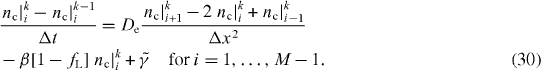
The electron diffusion through the nano-structured CNT film, with variable generation and recombination terms using appropriate boundary conditions, is evaluated. By illuminating the working electrode, electrons are injected in the system, resulting in an electron density build-up in the film that is a function of position and time. Electrons are allowed to diffuse towards the working electrode, which in turn behaves as a collecting interface. The continuity equation is finally solved by linear geometry, i.e. only the x-coordinate is considered [20]. The x denotes the location within the cell, where x = 0 indicates the TCO–CNT interface at the front electrode. The x = d indicates the interface between the electrolyte and Pt-TCO where d represents the thickness of the simulated cell; and nc is the density of free electrons in the conduction band. Hence, the following differential equation is solved:

where De is diffusion coefficient for electrons (m2 s−1); and G(x) is the generation rate at distance x, ne(x,t) is the total density of electrons (cm−3) as a function of time (t) and distance (x) from the working electrode [16], and neq is the carrier density of electrons at equilibrium in the dark.
Equation (8) is solved by FDM using the lax scheme [20, 21] and with the following two boundary conditions:
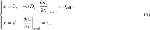
where q is elementary charge of the electron (1.6 × 10⁻¹⁹ C), and Jcell is short-circuit current density of the cell.
Considering that for t = 0 the cell is in the dark at equilibrium:

where t is exposure time in seconds.
The generations could be simplified in integral form (equation (11)), where α(λ) denotes the absorption coefficient, ninj is the electron injection efficiency, φ (λ ) the incident photon flux, and λ the wavelength:

Generation rates are integrated in the wavelength range from 300 (λmin) to 800 nm (λmax), where the DSSC is active [22], while on the other hand, they could also be a result of the optical simulator. At open circuit only recombination currents flow inside the cell. Electrons recombine with tri-iodide ions in the electrolyte, or enter the front TCO layer and recombine from there [23]. The electron transportation (recombination) to the tri-iodide species follows first-order kinetics as [16, 22]

where Re(x) is the rate of electron combination as a function of x, and τe is electron lifetime (s) determined by back reaction with redox couple I−/I3−.
The dark equilibrium carrier density neq corresponds to the matching between the Fermi level in the CNT and the Eredox. When the Fermi level is aligned with electrolyte potential (i.e. kept constant, because electrolyte concentrations are almost constant and their potential is nearly constant) this indicates that the carrier density is constant. Fermi level is affected by majority carrier density.
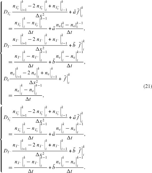
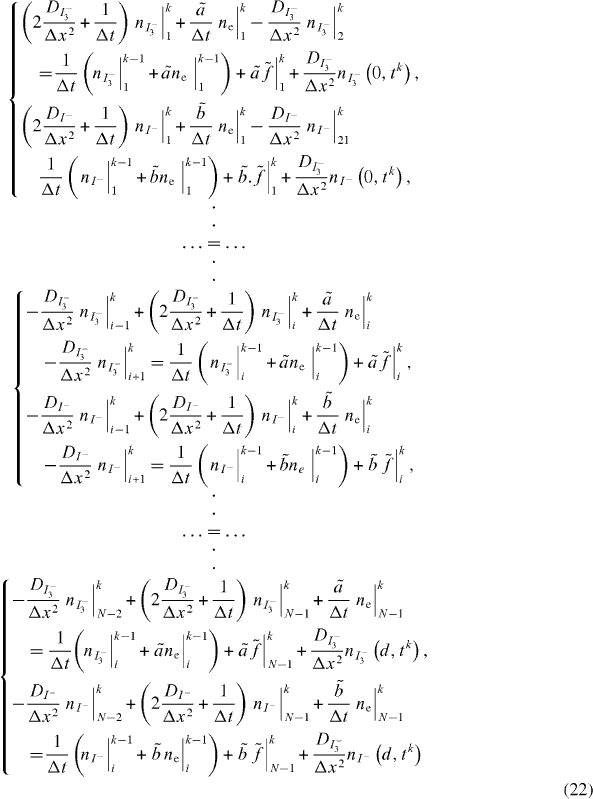
2.1.2. Charge transport in redox species (continuity equation for redox species).
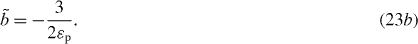
The oxidation of iodide ions and the reduction of tri-iodide occur inside the electrolyte species present in the interstitial space within the CNT nano-particles. Taking into account the stoichiometry of reactions (3) and (4), the terms of generation and recombination of tri-iodide and iodide species must be affected by the corresponding coefficients (1/2) and (−3/2), respectively:
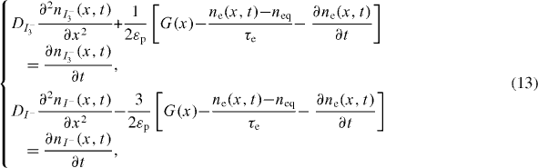
where DI3− and DI− are diffusion coefficients for ions I3− and I−, respectively; nI3− and nI− are concentrations for I− and I− ions, respectively (m−3); and εp is CNT film porosity.
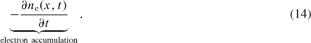
In a non-steady state, the accumulated electrons do not participate in the redox reactions and must thus be discounted from the ion generation term [16]
At time t = 0, initial concentrations of the electrolyte species are assumed:

At the TCO–CNT interface only the photo-injected electrons flow. The net flux of I− and I3− ions is zero, thus

The total amount of the redox species contained in the CNT nano-pores remains constant during the DSSC operation. This may be described as [24]

In this study, the approximate equations of nI3− (x,t), nI3− (x,t) and ne (x,t) are estimated using the FDM.
3. Numerical solutions of difference equations for various types of boundary conditions
3.1. Numerical solutions for electron transport in the CNT electrode
The platform, the so-called slice here, involves a number of sub-models. The sub-models describe the structure of the electrode, the generation of electrons and the contacts. They also describe the electron and ion mass transport processes, and the electron transfer reactions between the redox couple (I−/I3−) and the oxidized dye molecules [25].
In addition to transporting charge between respective interfaces, the electrolyte also influences electron transport within the nano-porous CNT [25–28]. The electrolyte has both redox and screening properties. Screening is directly coupled to the ionic ability to charge-compensate electrons in the nano-structured semiconductor.
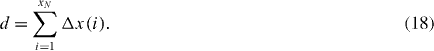
The cell is treated as a one-dimensional effective medium whose thickness, d, is divided into a number of slices, xN. The length of an individual slice is expressed as Δ xi = xi - xi - 1 = Δ x. The relation is expressed as
A sequence of slices is referred to as a region. A slice includes a generation region, an electron transport region and an electrolyte transport region. Figure 1 shows a schematic slice structure model corresponding to a DSSC. In the multiple trapping (MT) models, electron transport is assumed to occur via an extended state Ec. Furthermore, in the present numerical model, the recombination processes of electrons with tri-iodide ions and dye cations may occur in the cell under operation.

Figure 1. Description of the DSSC by the slice model, and illustration of the multiple-trapping model of transport (left) and the geometry used for solving the continuity equation (right). The cell is assumed to be a one-dimensional medium whose thickness, d, is divided into a number of slices, xN, where the length of each slice is Δ xi = xi - xi - 1 = Δ x.
Download figure:
Standard imageIn solving equation (8), for charge transport, the FDM will be used. For the sake of simplicity, it is assumed that the mesh with nodes in points 1,..., i, ..., N is homogeneous. Thus, Δ xi = xi - xi - 1 = Δ x = constant . The node with subscript 1 is located at the electrode surface, and the node with subscript N is located at the outer boundary of the diffusion layer.

with

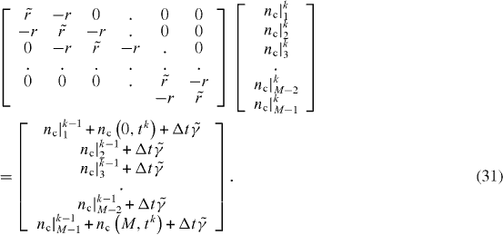
In the inner nodes of the mesh, for the spatial discretization of equations (19a) and (19b) of CNT electrode transfer, the central differences are used. Therefore
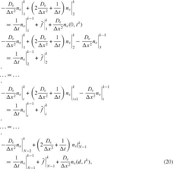
k designates the point order of the node in the mesh, and should not be confused with the Boltzmann constant which is denoted as kB elsewhere.
3.2. Numerical solutions for ion transport in the electrolyte

4. Numerical model for electron conductivity in nano-structured CNT semiconductors
The measured capacitance, which is believed to be a chemical type in nature as shown below, is affected by a number of parameters, as shown in figure 1 [29, 30]. Process (B) indicates polarization at the transparent conducting substrate (TCS)–electrolyte interface, and (C) indicates the Helmholtz layer at the oxide–electrolyte interface. The former effect is important when the electron density in the semiconductor is low [31] and the latter when the density is very high with semiconductor band unpinning. Both contributions can be thought of as ordinary electrostatic capacitors, where the charges in two highly conducting plates sustain an electrical field in between.
In the intermediate range of Fermi level variation, a different kind of capacitive effect is found, as shown in section (A) of figure 2. The semiconductor bands are pinned, and the charge accumulation is related to the displacement of the Fermi level position with respect to the conduction band edge. This means variation of the chemical potential of electrons as  . Hence, the increment of charge (both electronic and ionic) occurs inside the nano-structured electrode with no concomitant electrical field variation therein. This is because the electrical field is shielded near the TCS [31]. Therefore, free energy storage in the capacitor is due to chemical rather than electrostatic energy. Therefore, it is a chemical capacitor rather than an electrostatic one. The chemical capacitance ((A) in figure 2) is a major feature in CNT nano-structured electrodes. Besides, the chemical capacitance is a concept of crucial significance for solar cell applications, because it properly describes the splitting of Fermi levels caused by excitation of carriers in the light absorber material [30, 32, 33]. Considering the variation of the electron density upon a change in local chemical potential in a DSSC, the chemical capacitance occurs. Two components in equation (24) may be distinguished [34]. The first is related to the free conduction band electrons.

where Cch(cb) is the chemical capacitance in the conduction band; nc is the conduction band electron density; kB is the Boltzmann constant and T is the temperature (K).
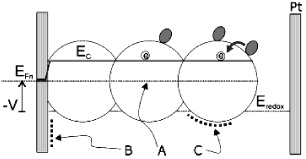
Figure 2. Schematics of the capacitive contributions in a DSSC: (A) Chemical capacitance due to increasing chemical potential (concentration) of electrons in the CNT phase, obtained when the electrode potential, V, displaces the electron Fermi level, EFn, with respect to the lower edge of the conduction band, Ec, in the semiconductor nanoparticles. (B) Electrostatic capacitance of the Helmholtz layer (and semiconductor band-bending) at the interface between the exposed surface of the transparent conducting oxide substrate and the electrolyte. (C) Electrostatic capacitance at the Helmholtz layer at the oxide–electrolyte interface.
Download figure:
Standard imageTo analyse these questions a relatively simple kinetic model is outlined for diffusion, trapping and interfacial charge transfer of electron carriers in a nano-structured semiconductor permeated with a redox electrolyte. We will use the MT model for transport and charge transfer illustrated earlier [16–18]. This model is adapted to nano-structured semiconductors from a wide experience on disordered semiconductors.
In the context of the MT model, the electron transport is carried out by a single kind of state, the extended states of the conduction band. Carriers trapped in localized states do not contribute to the dc conductivity until they are released again. The kinetic transport equations are stated in the MT model for a single kind of trap, involving the equations of conservation for free and trapped electrons [30]:

where Je is the electron flux and fL is the fractional occupancy (nL = NLfL, where NL is the density of traps); β is the symmetry coefficient; and γ is the rate constant for electron thermal release from the trap to the conduction band.
As explained before, diffusive transport of electrons within the CNT film towards the TCO is considered. Equation (26) relates the electron flux, Je, at any position x to the gradient of electron concentration across the CNT layer, ne, by means of the electron diffusion coefficient, De in Fick's law [22, 30]

The rate constant for electron capture is determined by the thermal velocity of free electrons, ν, the electron capture cross section of the trap, sn, and the overall density of traps, NL, as

where NL is the total density of localized sites.
The rate constant for electron thermal release from the trap to the conduction band, γ, is described by the Shockley–Read–Hall statistics

where Ec is the lower band edge energy, EL is the energy of the localized state in the band gap and Nc is the effective density of conduction band states. The occupancies, fL, in the two kinds of states are given explicitly by

Note that, in equation (29), the Fermi level  can be maintained at a value different from the redox potential in solution, Eredox [30].
In the one-dimensional case, considering the approximation of the theory of equations, electron conductivity transfer in dimensionless form can be written as follows:
In the inner nodes of the mesh, for the spatial discretization of equations (30) of electronic conductivity CNT transfer, the central differences are used. Therefore
Another important quantity for many applications is the electron conductivity, which can be simulated in the steady state as reported elsewhere. Using equation (24), the conductivity related to the electron diffusion process, σn, can be obtained from the generalized Einstein relation where μn is the chemical potential of electrons [30, 34] as

where D0 is the constant diffusion coefficient for free electrons.
5. Results and discussion
In order to validate the present numerical model, the simulation results are compared with the numerical results in the literature, particularly with TiO2-based DSSC performance results reported by Andrade et al [16]. All input parameters used in the simulation are shown in table 1.
Table 1. Simulator input parameters.
| Parameter | Value | Reference |
|---|---|---|
| AC | 0.158 cm2 | [16] |
| τe− | 23.6 ms | [16] |
| De− (electrode TiO2) | 1.10×10⁻⁴ cm2 s−1 | [16] |
| μe (electrode CNT) | 108 cm2 V−1 s−1 | [14] |
| De− (electrode CNT) |  |
[14] |
| DI− | 8.5×10⁻⁶ cm2 s−1 | [23] |
| DI3 − | 8.5×10⁻⁶ cm2 s−1 | [23] |
| NCB | 1.0×1021 cm−3 | [16] |
| ηinj | 0.90 | [16] |
| α (λ ) | 1000 cm−1 | [16] |
| εp | 5% | [37] |
| ϕ (λ ) | 1.0×1017 cm−2 s−1 | [38] |
| me* | 5.6×me | [23] |
| Resistivity (CNT) (300 K) | 0.1 Ω cm | [14] |
| T | 298 K | – |
| ECB−Eredox | 0.93 eV | [16] |
| nI3−0 | 2.71×020 cm−3 | [23] |
| nI3−0 | 3.01×1019 cm−3 | [23] |
| ne0 | 10×1010 cm−3 | [23] |
Figure 3 compares the evolution of the transient electron density profile obtained from the present simulation with the numerical results of the FDM. The plot shows that as the electron density distribution increases, the diffusion of the tri-iodide towards the electrode becomes more limiting. This is primarily due to their low initial concentration, with the limited density of 4.6 × 1017 cm−2 obtained for this case. The plot shows very good agreement with the numerical results obtained from FDM which forms the basis of the present model. Parametric studies based on the validated model are discussed here. Figure 3 shows the evolution of the electron density profiles under short-circuit conditions before reaching the steady-state condition.
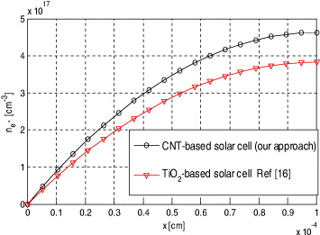
Figure 3. The distribution of the electrons within the simulated 1 × 10⁻⁴ cm thick active layer in CNT- and TiO2-based DSSCs.
Download figure:
Standard imageThe electron density profiles during the first micrometers of the TiO2 and CNT film steadily increase, becoming more flat afterwards. The active layer, presented by the finite difference method, is electrically modelled as a one-dimensional pseudo-homogeneous layer. The electro-active charge carriers included in the model are photo-generated free electrons (injected in nano-porous CNT), iodide and tri-iodide ions in the electrolyte. The structure of the DSSC is first divided into two different regions: the active layer (a mixture of electrolyte and nano-pores covered with dye which is treated as the pseudo-homogeneous layer) and the bulk electrolyte layer. Figures 3–5 show the distribution of the electrons, iodide and tri-iodide ions within the simulated 1 × 10⁻⁴ cm-thick active layer of DSSC under the short-circuit operation conditions. Figure 3 shows that the electron concentration distribution is much smaller under short-circuit conditions, since most of electrons reach the front contact. The first few micrometres of the CNT contribute most to the total JSC, while electrons generated deeper in the active layer partly recombine with tri-iodide ions. Therefore under short-circuit conditions, the electron concentration almost equals zero at the front contact and monotonically increases along the positive x-direction. I− ions are normally generated at the counter-electrode. Therefore, the concentration of I− ions monotonically decreases with decreasing x, figure 4. The role of iodide is to restore the positively charged photo-excited dye into its ground state. Consequently, under short-circuit conditions, the concentration of I− ions is smallest near the working electrode.
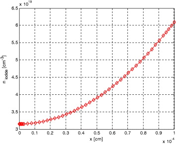
Figure 4. The distribution of the iodide ions within the simulated 1 × 10⁻⁴ cm thick active layer of the DSSC.
Download figure:
Standard image
Figure 5. The distribution of the tri-iodide ions within the simulated 1 × 10⁻⁴ cm thick active layer of the DSSC.
Download figure:
Standard imageOn the other hand, iodide could also be formed by a recombination process, especially under open-circuit conditions. Therefore, the concentration of I− ions becomes higher near the counter-electrode. The opposite is true for tri-iodide ions, which are formed at the working electrode and then diffuse towards the counter-electrode, as shown in figure 5. At the counter-electrode interface, the tri-iodide ions may recombine with free electrons. Therefore the concentration of tri-iodide ions monotonically decreases with increasing x.
The conductivity distribution profiles for CNT and TiO2 electrodes were studied. Conductivity profile results for CNT and TiO2 electrodes are shown in figures 6 and 7, respectively. The conductivity values were calculated by equations (31) and (32), using the finite-difference method simulation of the standard DSSC configuration. For the CNT case, figure 6 indicates that the conductivity of the semiconductor film varies over more than eight orders of magnitude, up to a maximum of 4.4 × 10⁻⁴ (Ω−1 cm−1) due to electron accumulation. As the electron concentration accumulates, at voltages less positive than the open-circuit voltage, an increase in conductivity is observed.
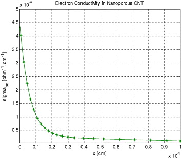
Figure 6. Evolution of electron conductivity in nano-porous CNT.
Download figure:
Standard image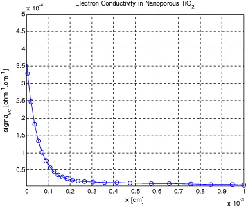
Figure 7. Evolution of electron conductivity in nano-porous TiO2.
Download figure:
Standard imageIt can be concluded that Ohmic contributions to the total current resulting from internal resistances, conductivity and diffusion affect the current in regions of larger positive or negative voltages. No significant similar influence appears under short-circuit current conditions. Interfacial reactions, dye coverage and total dye concentration do affect the short-circuit current. In the case of the interfacial rate constants, it appears that the total current is more influenced by the injection rate and electron returning rate than by any other interfacial reaction.
The distribution of the current–voltage (J–V) characteristics for DSSC having different series resistances (AC is the cell area, see table 1) can now be discussed. Under short-circuit conditions, the (total) electron density, at the working electrode (x = 0) and at zero time, is considered to be equal to the electron density at zero photovoltage, n0 = n(x = 0, V = 0, t = 0) = n(x = 0, V = 0,t). Under short-circuit conditions, electrons are easily extracted as a photocurrent and none of them is drawn to the counter-electrode directly. Therefore, the boundary conditions are

and
The short-circuit current density JSC can thus be obtained as
where q is the charge of an electron; L is the electron diffusion length that equals  ; and d is the thin film thickness [35, 36].
Cells with an external resistive load can be modelled if an appropriate functionality for the electron density at the working electrode is taken into account. In the presence of an applied voltage or under higher illumination intensity, the electron density in the film increases. Here, we compute the electron density as a function of voltage at x = 0, ne(V), as follows:

where  is a parameter that reflects the average depth of the distribution of the trap state energy below the conduction band.
For each defined external current density the cell voltage is calculated using equation (37), where V denotes the cell's voltage and ER(d) the redox potential at the counter-electrode. The EnF(0) is the Fermi level of the CNT at the TCO–CNT interface (x = 0), which is determined from the concentration of free electrons at the TCO–CNT interface, ne(0), equation (38). The NCB is the effective density of states in the CNT conduction band (equation (39)), where m*e is the effective electron mass and h is Planck's constant [22, 23]:


The presented model, which was implemented in a thin film solar cell simulator [1, 23], permits the steady-state simulation of the complete J–V characteristics, depth-dependent concentration of electro-active spices and their current densities in a DSSC. The numerical solution of the continuity equation (equation (8)), in combination with equations (36) and (37), and the boundary conditions, produces current–voltage curves that fit the diode equation with an ideality factor of unity. Thus, the solar cell behaves as an ideal diode at different series resistances. The calculated J–V characteristics of illuminated TiO2-DSSC [16] and CNT-DSSC-based solar cells (100 mW cm2, AM1.5) for different series resistances of TCO layer were introduced into the idealized simulated photo J–V characteristics. The results are presented in figures 8 and 9.
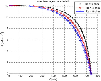
Figure 8. Calculated photo J–V characteristics for TiO2-DSSC-based solar cells with different series resistances of the TCO layer using the input parameters of [16].
Download figure:
Standard image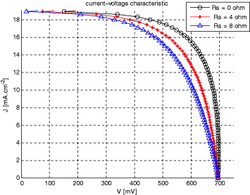
Figure 9. Calculated photo J–V characteristics for CNT-DSSC-based solar cell having different series resistances (our approach).
Download figure:
Standard imageBased on simulation results in a simple electrical model the calculated short-circuit current density (JSC) is 18.8 mA cm2 for CNT-based DSSC, compared with the values for TiO2-based based DSSC which are generally about 12.2 mA cm2. The calculated open-circuit voltage (VOC) is 700 mV for CNT-based DSSC, which is less than the VOC for TiO2-based DSSC. The FF was 69.30% for CNT-based DSSC, when the idealized cell without TCO resistance was simulated (RS = 0 Ω). The conversion efficiency of simulation results in a CNT-based solar cell without additional series resistance was 8.29%, compared with 7.02% for the TiO2-based counterpart. The difference is in agreement with expectations since the material parameters used in simulation are not optimized yet. Performance parameters for the two cell types are summarized in table 2 (entry 1). Unlike polycrystalline-based solar cells which exhibit carrier electron–hole recombination, which limits their efficiency, the CNT matrix (in CNT-based cells) serves as the conductor for majority carriers and prevents such a recombination. That is because of special conductivity and visible-near infrared transparency of the CNT.
Table 2. Performance parameters of simulated DSSC having different series resistances for CNT- and TiO2-based systems.
| JSC (mA cm−2) | VOC (mV) | FF (%) | η (%) | |||||
|---|---|---|---|---|---|---|---|---|
| RS (Ω) | CNT-based DSSC (our approach) | TiO2-based DSSC ([16]) | CNT-based DSSC (our approach) | TiO2-based DSSC ([16]) | CNT-based DSSC (our approach) | TiO2-based DSC ([16]) | CNT-based DSSC (our approach) | TiO2-based DSSC ([16]) |
| 0 | 18.8 | 12.2 | 700 | 740 | 69.30 | 68.91 | 8.29 | 7.02 |
| 4 | 18.8 | 12.2 | 700 | 740 | 62.68 | 62.95 | 7.49 | 6.11 |
| 8 | 18.8 | 12.2 | 700 | 740 | 54.25 | 60.16 | 6.49 | 5.70 |
Different series resistances were then introduced into the idealized simulated photo J–V characteristics for CNT-based DSSC. The results are again shown in figures 8 and 9 and are summarized in table 2 (entries 2–3). As expected, the JSC and VOC values did not change for either cell. In the CNT-based cell, the FF decreased from 69.30 to 62.68% when RS = 4 Ω was added, and to 54.25% when RS = 8 Ω was added. Consequently, the initial conversion efficiency was reduced from 8.29% to 7.49 and 6.49% when RS = 4 and 8 Ω were added, respectively. The TiO2-based cell also exhibited lowering in values of FF and conversion efficiency by adding series resistances, as shown in table 2.
6. Conclusion
A mathematical model for a new type of photovoltaic solar cell based on dye-sensitized CT electrodes is discussed. In contrast to conventional solar cells, where light absorption is due to band gap excitation of the semiconductor itself, the CNT with its wide band gap is transparent in the visible spectrum. While the efficiency of conventional polycrystalline solar cells is limited by charge carrier recombination at grain boundaries, bulk defects and impurities, the CNT serves only as the conductor for majority carriers (injected electrons), so that electron–hole recombination in the semiconductor is absent. The unique characteristics of carbon films as window electrodes are due to their excellent conductivity and good transparency in both visible and near-infrared regions.
The model describes charge transfer and charge transport within the porous CNT electrode of the DSSC.
Charge transfer at the semiconductor–dye–electrolyte interface within a DSSC is also described. The model is based on solving the continuity equation for electrons, using the numerical finite difference method. The equations were used to describe the charge transport within the electrolyte filled pores and the porous semiconductor.
Acknowledgments
YG and AC acknowledge Université Amar Telidji de Laghouat, Algérie, for financial support. HSH acknowledges the Al-Maqdisi Project for help.