


Abstract
We have clarified that a topological insulator, Bi2Te2Se, shows two surface states with gigantic Rashba-type spin-splitting located at a binding energy deeper than the topological surface state. The magnitude of the Rashba parameter, as well as the momentum splitting, is found to be large enough to realize a number of nanometer-sized spintronic devices. This novel finding paves the way to studies of gigantic Rashba systems that are suitable for future spintronic applications.
Export citation and abstract BibTeX RIS

Content from this work may be used under the terms of the Creative Commons Attribution 3.0 licence. Any further distribution of this work must maintain attribution to the author(s) and the title of the work, journal citation and DOI.
1. Introduction
Topological insulators and Rashba systems have attracted a great deal of attention as key materials to revolutionize spin current devices without external magnetic fields [1–4]. In these nonmagnetic materials, the spin degeneracy is lifted by spin-orbit interactions in combination with broken space inversion symmetry. These systems have been extensively studied in recent years by angle-resolved photoemission spectroscopy (ARPES), spin- and angle-resolved photoemission spectroscopy (spin-ARPES) and first-principles calculations [5–37]. In particular, the spin characteristics of the surface states have been discussed in detail. In ideal topological insulators and Rashba systems, the spins are completely oriented in-plane and normal to the electron momenta, forming a helical spin texture.
The ideal two-dimensional Rashba effect is explained by the Rashba Hamiltonian ( ) [6].

From the Hamiltonian, the Rashba effect leads to a spin-splitting of the parabolic band dispersion, as described below [6]

where,  and
and  are the effective mass and Rashba parameter. Here,
  and
and  are defined as
  and
and  . In many cases, the Rashba parameter
  is thought to be the most important for highly efficient spintronic devices such as spin-field-effect transistors (spin-FETs). Since the source–drain distance (L) of spin-FETs is required to be larger than the characteristic half-wavelength
  [2], and
  is directly linked to the stability of the device operated at elevated temperatures, one should also pay more attention to
  and
and  . In fact, the spin-splitting size needs to be more than
  = 0.1
= 0.1  and
and  = 200 meV in order to downsize the channel length to a few nanometers and to realize stable device operation at room temperature. However, the spin-splitting size is currently insufficient in the Rashba systems discovered so far, including the (111) surfaces of Au, Bi and Sb [6–13], as well as Bi/Ag(111)[14, 15] and bulk BiTeI, etc [16–20]. Therefore, as a first approach we need to discover Rashba systems with larger spin-splitting. In this context, topological insulators or similar compounds might have the potential to show a larger Rashba effect due to the much stronger spin-orbit interaction than in well-known Rashba systems.
Here, we present a deeper-lying surface state with gigantic Rashba spin-splitting in the topological insulator 
 Se, studied using state-of-the-art spin-ARPES. Previously, we clarified that the highly spin-polarized natures of topological surface states (TSSs) are persistent above and below the Dirac point in this material [23, 40]. These findings can be a platform for future studies on gigantic Rashba systems that are suitable for spintronic devices.
2. Experimental
The ARPES experiment was performed at the bending-magnet beam line (BL-7) with a hemispherical analyzer (VG Scienta SES 2002) at the Hiroshima Synchrotron Radiation Center (HSRC). The spin-ARPES experiment was done at the APPLE-II type variable polarization undulator beam line (BL-9B) at HSRC. Our spin-ARPES system is equipped with a hemispherical electron analyzer (VG Scienta R-4000) combined with a pair of very low energy electron diffraction (VLEED)-type spin detectors, and achieves much higher efficiency ( ) than conventional Mott-type spin detectors (
 ) [41]. The spin-ARPES system can resolve both out-of-plane (
 ) and in-plane (
 and
and  ) spin polarization components with high angular and energy resolutions, as schematically shown in figure 1(a). The signs of the polar (θ) and tilt angles (θt) of the sample are defined as positive, in the case of anticlockwise rotation about the x axis and clockwise rotation about the y axis, respectively. The overall energy and angular resolutions for ARPES (ARPES and spin-ARPES) were set to 40 meV (20 meV) and 0.3
 (0.75
(0.75 ) at BL-7 (BL-9B), and all measurements were performed at a sample temperature of 70 K. The samples were cleaved in-situ under an ultra-high vacuum below
  . ARPES at BL-7 was conducted using synchrotron radiation with photon energies (
 ) ranging from 21 to 60 eV. Spin-ARPES and ARPES at BL-9B were performed with a high-flux He-discharge lamp (
 = 21.22 eV).

Figure 1. (a) Schematic of our efficient, spin-resolved spectroscopy machine, and the experimental geometry. (b)–(e) The energy-band dispersion curves along  taken by a p-polarized synchrotron radiation light of
  = 21, 25, 30 and 46 eV.
Download figure:
Standard image High-resolution image3. Results and Discussion
Figures 1(b)–(e) show the selected ARPES results obtained by several photon energies along the  line. The energy dispersion curve taken at 21 eV shows two upward-convex parabolic states (dashed line), as well as another upward-convex arc, with the energy maximum at a binding energy (
 ) of 1.75 eV, at the
  point. In particular, two characteristic parabolic bands (
 ) with an energy maximum of
  = 0.75 eV and a wavenumber of
  are clearly observed, with a crossing at
  = 1.25 eV at the
  point. In figures 1(c)–(e), the results for
  = 25, 35 and 46 eV present one TSS near the Fermi energy, as already reported by several groups [23, 24] and the parabolic band structure (
 ) without changing band shape. The weak broad, bulk band structure (B) is also observed close to the
  state below 1.25 eV. Note that the particular parabolic band
  can be observed with all photon energies in our study as keeping the energy maxima, the crossing point at the same energy, and the same k-position, which confirms its two-dimensional nature. More interestingly, the surface state
  is likely to show extremely large Rashba-type spin-splitting.
The two-dimensional slices in the k space for TSS and  at several constant energies are shown in figure 2. Figure 2(b) demonstrates a typical hexagonal deformation of TSS, which evolves into a circular shape on approaching the crossing point. We find that the band dispersion along the
  line gradually becomes steeper toward
  , while it is almost straight along the
  line, which actually reflects the deformation of constant energy contours (CECs). Near the crossing point, the bulk valence band forms a six-fold petal-like pattern. These results are in agreement with a previous report for TSS [24]. The
  in figure 2(d) is also visible as the hexagonal-shaped CECs at
  = 0.75 eV. The CEC for the inner part of
  evolves into a circular shape upon approaching the crossing point (
 ), and again into a hexagonal-shape in going further to deeper
  , but the shape is rotated by 90
 with respect to the CEC above the crossing point. On the other hand, the outer part of
  exhibits a snowflake-like pattern down to 1 eV and disappears below 1 eV. Here, we find that the characteristic deformation is abnormal for
  at the band top, and is rotated by 90° with respect to the TSS.
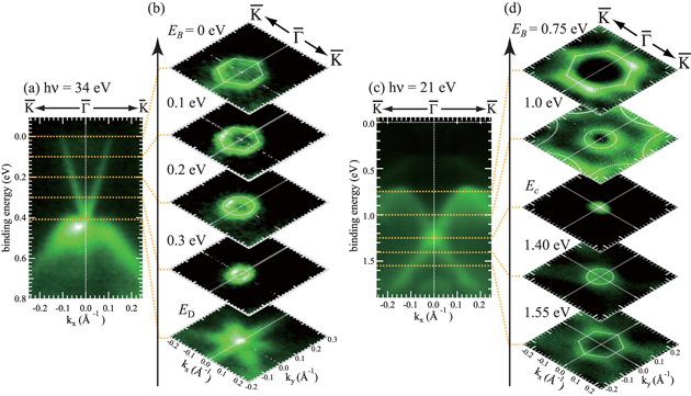
Figure 2. (a), (c) ARPES results taken by p-polarized light of two photon energies ( ) suitable for the observation of TSS and
  along
along  . (b), (d) The constant energy contours for two different surface states at several binding energies from 0 to 0.41 eV and from 0.75 to 1.55 eV.
Download figure:
Standard image High-resolution imageTo unravel the spin characteristics of  , we performed the spin-ARPES measurement excited with unpolarized He
  light (
 = 21.223 eV). Figure 3(a) shows the spin-resolved energy distribution curves (EDCs) for
  = 0-2.3 eV for several emission angles along the
  line. Here, spin-up and spin-down spectra are plotted with upright and inverted triangles, respectively. In the EDC for normal emission, two features are observed at
  = 1.75 and 1.25 eV in both spin channels. The peak around 1.75 eV shifts to higher
  as
as  increases. Since these features are almost spin degenerate and the band shape also changes as a function of
  , as shown in figures 1(b)–(e), this can be assigned to the bulk-derived state. For the prominent
  state, the spin-up peak shifts to higher
  with increasing θ from 0 to 2.3°, and splits into two branches from 3.8
 . We also notice that one spin-down branch shifts to lower
  and another branch moves to lower
  up to 0.7
 and higher
  above 0.7
 . For negative θ, we observe the same
  dispersion but with opposite spin polarization signs. This result clearly shows that the
  band is spin-split and the spin orientation is antisymmetric with respect to the
  point. We also find that the lower-
 branch of
  is followed by weak features of the opposite spin spectra in the limited range of theta (−5.3
  θ
θ
 −1.3, 2.3
  θ
θ  5.3), as indicated by the open circles. The intensities of these peaks do not exceed those for the opposite spin channel at the same
  , even if the photon energy is changed (not shown here). Moreover, we can observe a shoulder structure for the opposite spin channel at the same
  as the weak peak indicated by the circles at θ =
  . This result implies that these peaks have no spin polarization. We believe that the lower-
 branch of
  stems from a bulk state corresponding to the weak broad structure (B) shown in figures 1(b)–(e). In figures 3(b), we assigned spin characters to the dominant spectral features in the contour plot using upright and inverted triangles. It is identified that there is another spin-split band (
 ). This
  state is not clearly noticed from the ARPES results in figure 1, because it overlaps considerably with the
  band in a wide momentum range, and the relevant spectral weight is weak. The
  state also shows a spin-splitting with an antisymmetric spin orientation with respect to the
  point.
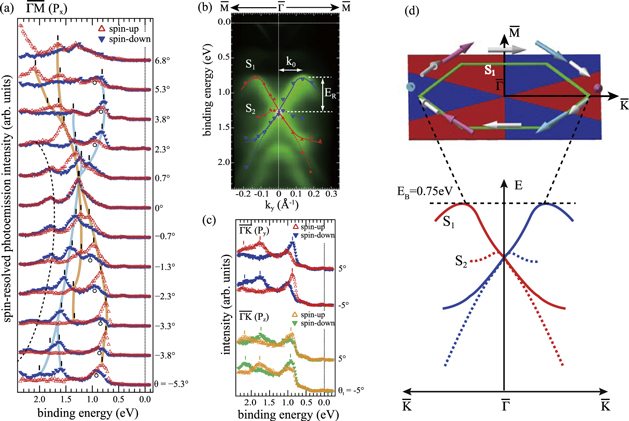
Figure 3. (a) Spin-resolved energy distribution curves (EDCs) of 
 Se along
  obtained by unpolarized He-Iα radiation. (b) The spin characters derived from the spin-resolved spectra in figure 3(a) are superimposed in E-k mapping by ARPES measurements with a He discharge lamp. (c) Spin-resolved EDCs along
  by unpolarized He-Iα radiation for spin components of
  and
and  . The schematic diagrams of (d) show band dispersion along
  (bottom part), and a two-dimensional map (top part) for the
  band and its spin orientations. The arrows indicate the spin orientation for the
  state, and the red (blue) and white colors show the positive (negative) and zero values of the out-of-plane spin polarization, respectively.
Download figure:
Standard image High-resolution imageAs the most important experimental finding, the spin polarized band  is found to show gigantic Rashba spin-splitting. Now, we try to get more insight into this particular band. Generally, the Rashba Hamiltonian without considering crystal symmetry is given by equation (1). In many cases, the Rashba parameter representing the magnitude of Rashba spin-splitting is experimentally estimated by
  from the ARPES results. In the present material,
  and
and  are 0.5 eV and
  , respectively. Using these values, we can estimate
  , which is more than twice as large as the reported value for the 'giant Rashba system' [14, 18, 19]. Moreover, the more important parameters
  and
and  show sufficient magnitudes to realize a few nanometer-sized spin current devices operated at room temperature. The Rashba spin-split band with such large
  and
and  has thus been discovered for the first time, and we call this the 'gigantic Rashba effect'.
Next, we perform the spin-ARPES measurement of the Rashba spin-split band along  to explore its spin texture, as shown in figure 3(c). Here, the effective Hamiltonian of the spin-orbit interaction with a combination of three-fold symmetry is expressed by [36]

Here,  and
and  correspond to the wave vectors along the
  and
and  directions, and
  . When the warping parameter
  is non-zero, a deformation of CECs takes place and the out-of-plane spin component emerges in the spin-split band along
  at the same time. Figure 3(c) shows that the spin-ARPES results resolve the in-plane (
 ) and out-of-plane (
 ) spin components at θ =
  , corresponding to the wavenumber near the top of the
  band along
  . The in-plane spin-resolved EDC at θ = 5° in figure 3(c) shows the spin-up and spin-down peaks at 1.75 and 0.85 eV, respectively, both of which correspond to the spin-split
  band, while the spin-up peak at 2.2 eV comes from the
  state. It is also noted that the spin-up and spin-down peaks of the
  state show a distinct out-of-plane spin component. This result implies that the observed deformation of CECs is explained by a hexagonal warping effect, as represented by equation (3). Figure 3(d) schematically shows the experimentally observed spin texture. Here, the arrows exhibit spin vectors determined from our spin-ARPES result by taking the
  crystal symmetry into account. The red (blue) and white colors show the positive (negative) and zero values of the out-of-plane spin polarization, respectively. The out-of-plane spin component takes a maximum at the
  direction and the in-plane spin component shows a helical spin texture. The spin features and CECs for each surface state resemble Bi/Ag(111), which is well known to show the giant Rashba effect. A strong in-plane potential gradient related to the warping parameter
  might also be a trigger of the gigantic Rashba effect in this system, as theoretically explained for Bi/Ag(111) [14, 36, 42]. Moreover, the sign of the in-plane spin component for the
  state at 1.75 eV is identical to that for the
  state located at 2.2 eV. Nevertheless, each out-of-plane spin component becomes the opposite. The difference in the out-of-plane spin component for
  and
and  implies that the sign of
  for
for  is reversed in comparison with that of
  . The origin of the observed sign reversal in the out-of-plane spin polarizations is unknown at present. However, if we assume that the charge densities of
  and
and  residing at the topmost and bottom Te (Bi) layers in one quintuple layer on the surface or vice versa are rotated 180
 to each other, then the out-of-spin polarization could change its sign. Different orbital symmetries could also explain the observed sign reversal.
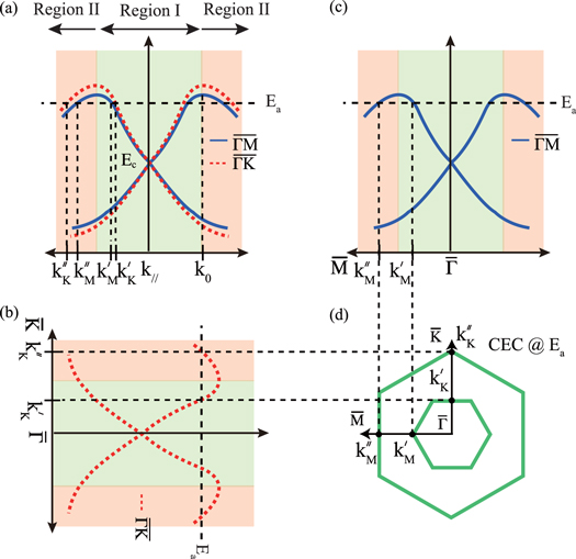
Finally, we discuss the hexagonal deformation in CECs of  , which is rotated by 90
 with respect to that for TSS. At one constant energy (
 ) above the crossing point, as shown in figure 4(a)–(c), the band dispersion along the
  line (
 line) crosses two points,
  and
and  (
( and
and  ). In figure 4(a), the band dispersion along the
  line is steeper than that along the
  for
for  (Region I), and thus
  becomes longer than
  . On the other hand, for
  (Region II),
  becomes smaller than
  . Consequently, the observed CECs are different in two regions. (1) In the region of
  , the CEC shows a hexagonal shape with vertices in the
  line, as is typically found for TSS. (2) For
  , the hexagonal shape or snowflake-like pattern of CEC is rotated by 90
 . The resulting constant energy contours at
  are drawn in figure 4(d). As one can see from figure 4(b)–(d), the outer CEC (Region II) shows a hexagonal shape that is rotated by 90
 with respect to the inner one (Region I) and also to the TSS (see figure 2(a)). The two CECs are merged into one around the top of the band. By considering the fact that the outer CEC shows a stronger spectral weight than that of the inner one, which is probably due to the photoemission matrix element effect, we can understand that the anisotropic constant energy contour at 0.75 eV for
  is rotated by 90
 with respect to those of TSS and
  at 1.55 eV, as shown in figure 2.
Figure 4. (a)–(c) Schematic figure for the Rashba spin-split band along  (dashed line) and
  (solid line). (d) The anisotropic constant energy contours (CECs) at
  .
.
Download figure:
Standard image High-resolution image
4. Summary
Gigantic Rashba spin-split bands have been observed in the topological insulator 
 Se by the ARPES and spin-ARPES experiments. The two-dimensional constant energy contours, as well as their spin textures, clearly show the peculiarity in the warping effect. Importantly, the magnitude of the Rashba parameter is found to be large enough to realize a few nanometer-sized spin current electronic devices. Moreover, two different spin-split
  and
and  states possess warping parameters with the opposite sign, even in the same crystal. This novel finding opens a pathway to studies of exotic electrical and optical phenomena driven by the gigantic Rashba effect.
Acknowledgments
The ARPES and spin-ARPES experiments were performed with the approval of the Proposal Assessing Committee of HSRC (proposal nos. 12-A-28, 12-B-16 and 13-A-23). A portion of this work has been done under the Japan–Russia Bilateral Joint Research Project (JSPS). This work was financially supported by KAKENHI (grant nos. 23340105, 23244066, 25800179), Grant-in-Aid for Scientific Research (A), (B) and for Young Scientists (B) of JSPS. KAK and OET acknowledge financial support by the RFBR (grant nos. 13-02-92105 and 12-02-00226), and by the Ministry of Education and Science of the Russian Federation.