


Abstract
Transport of plasmons in graphene has been investigated by time-resolved electrical measurements. We demonstrate that the velocity v (or the refractive index  ) and the characteristic impedance Z of the plasmon mode can be tuned through the carrier density. By exploiting the Z tunability, we present a gate-defined plasmonic waveguide. An important advantage of the gate-defined waveguide is dynamical switching of guiding characteristics with the gate voltages. One can tailor the patterns of gate electrodes to define two output waveguides branching off from a source waveguide, and the output waveguide can be switched by changing the gate voltages. Indeed, we show the routing in a Y-shaped channel: the path for the plasmon transmission can be selected by tuning Z of each path. These results can be well reproduced by simulation, encouraging the design of graphene-based plasmonic devices.
Export citation and abstract BibTeX RIS

Content from this work may be used under the terms of the Creative Commons Attribution 3.0 licence. Any further distribution of this work must maintain attribution to the author(s) and the title of the work, journal citation and DOI.
1. Introduction
When fluctuations appear in the density of charge carriers in metals and semiconductors, Coulomb restoring force leads to collective charge oscillations, i.e., plasmons. Recently, plasmons in graphene [1, 2] have attracted interest, particularly because of the tunability of plasmon properties by means of electric-field doping. The plasma frequency depends on the carrier (electron or hole) density n as  [3], as has been confirmed by the tunable resonant frequency in micro-ribbon structures [4] and optical nano-imaging [5, 6]. Theory predicts that plasmons can be guided along patterned gate electrodes with appropriate voltages: Vakil and Engheta pointed out that plasmon waveguide can be formed by changing the sign of the imaginary part of conductivity at terahertz frequencies [7], while Mischenko et al suggested the existence of plasmon modes along a p-n junction [8]. The guiding is also possible by using edge magnetoplasmons, which travel along the graphene edge in a perpendicular magnetic field B. By exploiting one-dimensional chiral transport and the long decay length of edge magnetoplasmons, a plasmonic circulator and gyrator have been proposed [9]. Experimentally, although the one-dimensional transport of edge magnetoplasmons have been observed [10–12], plasmon guiding in the absence of B has not been demonstrated yet.
Here, we propose and demonstrate that a plasmonic waveguide can be formed by spatially modulating n at B = 0. The refractive characteristics are determined by the velocity v and impedance Z of plasmon mode in graphene, which can be tuned through n. We carried out time-resolved charge-transport measurements to investigate the transport properties of plasmons. Fundamental characteristics of v and Z are tested using a graphene device with a uniform gate. To demonstrate the plasmonic waveguide, a gate-patterned device is used. The waveguide characteristics are confirmed with an enhanced signal at the output of the channel, but suppressed signals pass through the side regions. The guiding effect is supported by numerical simulations. Taking advantage of the electrical tuning of the waveguide, we also demonstrate a Y-shaped routing device, in which an incident wave is selectively routed to one of the two output waveguides. A waveguide that does not require an electric or plasmonic bandgap is attractive for developing graphene-based plasmonic devices.
2. Experimental setup
The devices were fabricated from graphene grown on SiC [13]. We prepared a graphene wafer by thermal decomposition of a 6 H-SiC(0001) substrate. SiC substrates were annealed at around  in Ar at a pressure of less than 100 Torr. For the fabrication of devices, graphene was patterned into multi-terminal geometry by etching in an
  atmosphere. After the etching, Cr/Au electrodes were deposited for Ohmic contacts. Then the surface was covered with 100 nm thick hydrogen silsesquioxane and 60 nm thick
  insulating layers. For gates, Cr/Au was deposited on the insulating layers. Dc transport measurement in the magnetic field shows well-developed
  , 6, and 10 quantum Hall states for
  T (see section 1 of the supplementary information, available from stacks.iop.org/njp/16/063055/mmedia), demonstrating the high quality of the SiC graphene. In our SiC graphene devices, n changes with the gate bias as
 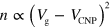 because of the large quantum capacitance of the interface state [17, 18], where
  V is the gate bias at the charge neutrality point (CNP). Hereafter we represent the gate bias as the bias measured from the CNP (
 ). The range of n in this experiment is between
 of electrons and
 of holes. As shown in the inset of figure 1(a), the uniform gate device consists of a
  patterned graphene (gray region), five Ohmic contact (orange regions), a top gate (green regions), and a gate to inject plasmons (pink region). Waveguide and routing devices have different gate or graphene structures, as shown in figures 2(a), 4(a) and 4(e).
Figure 1. (a)  for
for  (red) and 40 V (black). The sharp peak at zero time delay is due to direct crosstalk. The broad peak that appears with a time delay is due to plasmons. The inset shows a schematic illustration of the graphene device with a uniform gate. The graphene is roughly
  square. Plasmons are excited by applying a voltage step to the injection gate and detected through three of the five contacts (D1, D2, and D3); the two other contacts (D1' and D3') are grounded. (b) The propagation velocity (red trace) of the plasmon wave packet as a function of
  . The vertical bar represents the typical error for the determination of the velocity. The black dashed and solid traces are the result of the calculation using the distributed circuit model with and without the R component. The blue trace represents R obtained by standard Dc transport measurement.
Download figure:
Standard image High-resolution image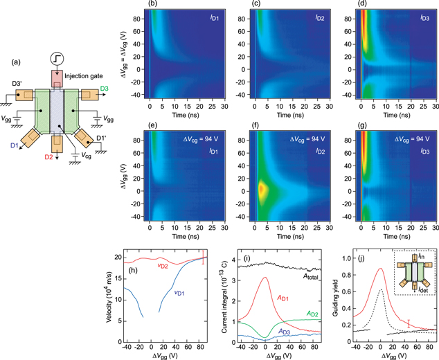
Figure 2. (a) Schematic illustration of the waveguide device with side guiding gates (green) and a center channel gate (blue). The width of the channel gate is 50  . (b)–(d) I as a function of time and the gate bias (
 ) detected through D1–D3, respectively. (e)–(g) I as a function of time and
  at a fixed
  V detected through D1–D3, respectively. (h) Propagation velocity of the plasmon wave packet obtained from
  (
( : blue trace) and
  (
( : red trace) as a function of
  . The channel gate bias is fixed at
  V. (i) Current integral
  and (j) guiding yield at
  V as a function of
  (red trace). As a reference,
  for
for  obtained from (b)–(d) is plotted (black solid trace). Because of the long time of flight and the limitation of the integration time rage, reliable
  cannot be obtained around
  V. The dashed trace in (j) represents the guiding yield obtained by a Dc measurement using the sample illustrated in the inset. The error for the guiding yield comes from the error in
  .
.
Download figure:
Standard image High-resolution image
Figure 4. (a) Schematic illustration of the routing device consisting of the Y-shaped channel, a channel gate (blue), and two routing gates (yellow). The width of the channel is  . (b), (c) A as a function of
  and
and  , respectively.
  and the other routing gate bias (
 for (b) and
  for (c)) are fixed at 71 V. (d) Routing yield obtained from the data in (c). (e) Sample structure for the routing in gate-defined channels. The sample has three guiding gates (green), one channel gate (blue), and two routing gates (yellow). (f) A as a function of
  .
.  ,
,  and
and  are fixed at 74 V. (g) A as a function of
  .
.  and
and  are fixed at 94 V, while
  is fixed at 0 V. (h) Routing yield obtained from the data in (g). To calculate the routing yield, we assumed
  C.
C.
Download figure:
Standard image High-resolution imageTime-resolved charge-transport measurements have been developed to estimate the drift velocity in silicon [14, 15], as well as the velocity of edge magnetoplasmons in GaAs [16] and graphene [10, 11]. We applied such a cryogenic high-speed electrical measurement to investigate plasmon transport in guided graphene devices. We performed the measurement in a GHz frequency range. Excess charge is induced by applying a voltage step with the height of 2 V to the injection gate. The temporal width of the charge is expected to be several hundred picoseconds. The pulsed charge travels in the graphene sheet dispersively as a plasmon mode. Then the pulsed charge flowing to the Ohmic contacts is measured by a sampling oscilloscope as the time-dependent current I(t) [10]. The effective path lengths from the injector to detectors are  for D1 and D1',
  for D2, and
  for D3 and D3', neglecting the length in ungated regions with much higher plasmon velocity. Experiments were performed at 1.5 K.
3. Results
3.1. Electrical control of plasmon velocity
To start, we show results for the plasmon transport in the uniform gate device. Figure 1(a) shows the current through the D2 detector  for
for  and 40 V (
 and
and  are presented in section 2 of the supplementary information). The sharp peak at zero time delay is due to direct crosstalk between high-frequency lines. The plasmon signal appears as a broad peak with a time delay. The slowly decaying tail is due to the time constant of the detection and, as will be discussed below, nonlinear plasmon dispersion induced by the resistance R of graphene. The time delay, which roughly corresponds to the time of flight of the plasmon pulse (section 3 of the supplementary information), increases with decreasing
  . The red trace in figure 1(b) shows the propagation velocity of the plasmon wave packet obtained from the time of flight and the path length as a function of
  . When
  is large, the velocity is of the order of
  . The velocity decreases with decreasing
  and varies almost symmetrically with respect to the CNP (
 ).
).
The  dependence of the plasmon velocity can be explained by a distributed constant circuit model. The response of charge carriers in graphene to the high-frequency electric field is characterized by the impedance
  , where L is the kinetic inductance arising from the inertia of charge carriers [19]. Since the carrier dynamics depends on n, L can be modified by changing n as
  with the effective mass
  in graphene. Including the capacitive coupling to the metal gate (inset of figure 1(b)), the wave equation for the propagation along the x axis becomes

where C is the capacitance to the metal gate and V is the potential induced by excess carriers in graphene. This gives the plasmon dispersion,

Using equation (2), we simulate a propagation of a plasmon wave packet (details of the simulation are given in section 4 of the supplementary information). For the simulation, we assumed a Gaussian wave packet with the full width at half maximum of 666 ps. We used 
 and
and  ; R is obtained by a phenomenological Lorenzian fitting to the measured resistance (blue trace in figure 1(b)), while C is determined by the geometry. Then, by setting
  , the calculated velocity reproduces the experimental result well (black line in figure 1(b)). When
  is large,
  at a typical wave number of our experimental condition
 (section 5 of the supplementary information). In this regime, the dispersion is almost linear
  and
and  depends on n as
  (dashed trace in figure 1(b)), consistent with [3, 20]. For
  V, on the other hand, the main component of k in the initial wave packet satisfies
  . In such a regime, charge excitations propagate diffusively rather than as traveling waves and thus the charge velocity is strongly reduced. It should be noted that the value of L used in the simulation is about 100 times larger than the value expected by
  , where
  is the Fermi velocity and e is the electron charge. We suggest that the enlargement of L, or correspondingly the suppression of
  , is due to the screening of the electron charge by the interface state between the graphene and SiC substrate. By the strong but not perfect screening, the effective charge
  for plasmons is reduced by a factor
  , where
  is the quantum capacitance of the interface state. Using
  deduced in [18],
  is estimated to be one order of magnitude smaller than e [21]. This is consistent with the enhancement of
  .
.
An important implication of the distributed RLC circuit model is that the Z obtained from equation (1) also depends on L and thus n as

Z increases with decreasing n: when R is small, it varies as  . Since the reflection coefficient between two media increases with the difference in Z of the media, the tunability of Z suggests that it is possible to form a plasmonic waveguide by tailoring n.
3.2. Plasmon guiding
Next, we show results for a sample with three parallel top gates (figure 2(a)). The two side gates (guiding gates) and the center gate (channel gate) serve to define the channel for the plasmon transport and change the properties of guided plasmons, respectively. By changing the guiding gate bias  and the channel gate bias
  independently, spatial distribution of n can be tuned. The gap between the gates is
  , in which n is fixed at the value for
  . Before demonstrating the guiding effect, we evaluate how the gap between the gates affects the plasmon transport. This can be done by measuring the current at the three detectors while applying the same gate bias to the guiding and channel gates (
 ). The results are shown in figures 2(b)–(d). At a constant bias,
  is largest, while
  and
and  are almost the same, consistent with the difference in the path length between the injector and each detector. As the bias is decreased, the time position of the current peak for all the detectors shifts to larger delays and the current pulse becomes broad, similar to the behavior observed in the sample with the uniform gate. These results indicate that the gap between the gates hardly affects the plasmon transport. This is reasonable because the gap is much smaller than the typical plasmon wavelength of
  .
.
When the spatial modulation is induced by applying different biases to the guiding and channel gates, the behavior becomes qualitatively different. Figures 2(e)–(g) show the current at the three detectors as a function of  at a fixed channel gate bias
  . When the guiding-gate region is tuned closer to the CNP, the plasmon signal in
  becomes larger, while that in
  and
and  almost disappears. This indicates that plasmons are guided in the channel defined by gates from the injector to detector D2. Figure 2(h) shows the plasmon velocity in the channel derived from
  (
( ) and in the guiding-gate region derived from
  (
( ) as a function of
  .
.  is about
  and depends on
  only weakly. On the other hand,
  decreases with decreasing
  , reflecting the n dependence of the velocity in the guiding-gate region. These results demonstrate that Z is modulated spatially and a plasmonic waveguide can be formed by applying different voltages to local gates.
To evaluate the yield of the guiding quantitatively, we calculated the current integral  , which represents the amount of plasmon charge arriving at each detector (figure 2(i)). Then the guiding yield is defined as
  , where
  is the total injected charge; since the sample has bilateral symmetry,
  [
[ ] is expected to be the same as
  [
[ ] and thus
  . In a uniform system (
 ), the guiding effect is absent and
  is almost constant at
  (black solid line in figure 2(j)). When the spatial modulation is induced, on the other hand,
  monotonically increases with decreasing
  and reaches the maximum value of 0.87 at
  V (red solid line in figure 2(j)). It is important to note that, although the guiding effect is partially due to the modulation of R through n in the guiding-gate region, the value
  is larger than the guiding yield for Dc current [22]. The dashed line in figure 2(j) represents the ratio of the injected and detected currents
  obtained by a Dc measurement using a sample with the same gate structure (section 1 of the supplementary information).
  is smaller than
  , indicating that the modulation of Z plays an essential role in the plasmon guiding.
We carried out similar measurements for several values of  (figure 3).
  is maximized by setting the guiding-gate region at the CNP and the maximum value increases with
  . The data are almost symmetric with respect to
  V and
V and  V, indicating that the guiding effect does not depend (or at least depends only weakly) on the carrier type. The velocity of guided plasmons, that is,
  at
at  V, increases with
  . The variation of
  at
at  V indicates that the velocity of guided plasmons is controllable. Note that, in principle, it is possible to guide plasmons by setting n in the channel smaller than that in the guiding-gate region. However, in such density distribution, R in the channel is large and thus plasmon damping is strong.
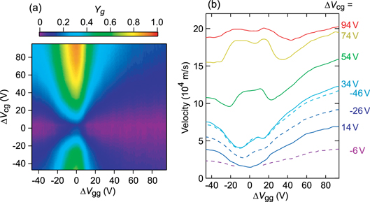
Figure 3. (a)  as a function of
  and
and  . (b)
. (b)  as a function of
  for several values of
  .
.
Download figure:
Standard image High-resolution image3.3. Plasmon routing
An important advantage of the gate-tunable guiding is that it is possible to change the route of the guiding channel simply by changing local gate biases. We demonstrate the plasmon routing using a sample consisting of a Y-shaped channel defined by etching, a channel gate, and two routing gates covering the branches of the channel (figure 4(a)). The routing gates serve to select the branch for the plasmon transport. In figure 4(b),  and
and  are plotted as a function of the D2 routing gate bias
  . During the measurement, biases of the channel gate and the other routing gate are fixed at
  . When
  too,
too,  and
and  are almost the same. As
  is decreased,
  decreases and, at the same time,
  increases. This demonstrates the plasmon routing to detector D1. The routing to detector D2 is also possible by changing
  (figure 4(c)). The routing yield, defined as

reaches 0.94 (figure 4(d)). The plasmon routing is also possible in a square-shaped device using guiding gates (figure 4(e)). By setting  V, the Y-shaped channel is defined (figure 4(f)). Then, by sweeping one of the routing gates, the routing is achieved (figures 4(g) and (h)). These results indicate that plasmons can be guided in a bent channel (section 6 of the supplementary information). As the ratio of
  to
to  can be tuned, the system can also work as a plasmonic switch, splitter, and intensity modulator.
4. Discussion
To investigate the guiding mechanism quantitatively, we simulated the time evolution of the plasmon potential using equation (1) (section 4 of the supplementary information). Figures 5(a) and (b) show snapshots of the plasmon potential at a time delay of 1 ns. In a uniform system at  , plasmons spread isotropically. When the guiding channel is formed by setting
  and
and  , plasmons are transmitted in the channel preferentially, and prevented from leaving it. The plasmon potential in the channel is much larger than that in a uniform system, manifesting the guiding effect. Figure 5(c) shows the plasmon potential for
  V at a point
  from the injection point as a function of
  and time. As expected, the amplitude of the signal increases with decreasing
  . The guiding yield obtained by the simulation is
  (figure 5(d)), which is very similar to the experimental result
  . The propagation velocity obtained from the peak position of the plasmon pulse also agrees well with the measured velocity (figure 5(e)). The
  dependence of the velocity comes from the fact that Z and thus the reflection coefficient between the channel and guiding-gate regions depend on k (equation (3)). This fact together with the nonlinear dispersion leads to the variation of the velocity.
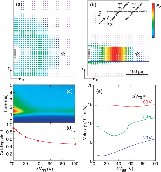
Figure 5. Results of simulation of plasmon guiding. (a), (b) Snap shot of the plasmon transport in a system for  and
and  , respectively, at a time delay of 1 ns. The size and the color of the dots represent the potential at each node of the distributed constant circuit (inset of (b)). The distance between the nodes is
  . The RLC component in the
  unit is
  for
for  and
and  for
for  . Plasmons are injected from the leftmost five points (black open dots). The waveform of the injected plasmons is a Gaussian with the full width at half maximum of 666 ps. Blue lines in (b) indicate boundaries between the channel and guiding-gate regions. (c) Plasmon potential at a point
  from the injector (open stars in (a) and (b)) for
  V as a function of
  and time. (d) Guiding yield for
  as a function of
  . (e) Propagation velocity of the plasmon wave packet in the channel for
  , 50, and 20 V as a function of
  .
.
Download figure:
Standard image High-resolution image
Acknowledgments
The authors are grateful to M Notomi and H Irie for fruitful discussion and M Ueki for experimental support. This work was supported in part by Grants-in-Aid for Scientific Research (21000004) and (21246006).