


Abstract
Phosphorene, a honeycomb structure of black phosphorus, was isolated recently. The band structure is highly anisotropic, where the kx direction is Dirac-like and the ky direction is Schrödinger-like. A prominent feature is the presence of a quasi-flat edge band entirely detached from the bulk band in phosphorene nanoribbons. We explore the mechanism of the emergence of the quasi-flat band by employing the topological argument invented to explain successfully the flat band familiar in graphene. The quasi-flat band can be controlled by applying in-plane electric field perpendicular to the ribbon direction. The conductance is switched off above a critical electric field, which acts as a field-effect transistor.
Export citation and abstract BibTeX RIS

Content from this work may be used under the terms of the Creative Commons Attribution 3.0 licence. Any further distribution of this work must maintain attribution to the author(s) and the title of the work, journal citation and DOI.
1. Introduction
Graphene is one of the most fascinating materials found in this decade [1, 2]. The low-energy theory is described by massless Dirac fermions, which leads to various remarkable electrical properties. In practical applications to current semiconductor technology, however, we need a finite band gap in which electrons cannot exist freely. For instance, armchair graphene nanoribbons have a finite gap depending on their width [3–5], while bilayer graphene under a perpendicular electric field also has a gap [6]. It is desirable to find an atomic monolayer bulk sample that has a finite gap. Silicene is a promising candidate for post graphene materials, which is predicted to be a quantum spin-Hall insulator [7]. Nevertheless, silicene has so far been synthesized only on metallic surfaces [8–10]. Another promising candidate is a transition metal dichalcogenides such as molybdenite [11–13].
A newcomer challenges the race of the post-graphene materials. That is phosphorene, a honeycomb structure of black phosphorus. It has been successfully generated in the laboratory [14–18] and has revealed a great potential in applications to electronics. Black phosphorus is a layered material where individual atomic layers are stacked together by Van der Waals interactions. Just as graphene can be isolated by peeling graphite, phosphorene can be similarly isolated from black phosphorus by the mechanical exfoliation method. As a key structure it is not planer but puckered due to the sp3 hybridization, as shown in figure 1. There are already several works based on first-principle calculations on phosphorene [19–22] and its nanoribbon [23–27]. The edge states detouched from the bulk band have been found in pristine zigzag phosphorene nanoribbons [24–27]. The tight-binding model was proposed [28] very recently by including the transfer energy ti over the five neighbor hopping sites ( ), as illustrated in figure 1.

Figure 1. Illustration of the structure and the transfer energy ti of phosphorene. (a) Bird eyeʼs view. (b) Side view. (c) Top view. The left edge is zigzag while the right edge is beard as a nanoribbon. Red (blue) balls represent phosphorus atoms in the upper (lower) layer. A dotted (solid) rectangular denote the unit cell of the four-band (two-band) model. The parameters of the unit cell length and angles of bonds are taken from [17].
Download figure:
Standard image High-resolution imageA striking property of phosphorene nanoribbon is the presence of a quasi-flat edge band [24–27] that is entirely detached from the bulk band. We explore the band structure of phosphorene nanoribbon analytically and numerically as a continuous deformation of the honeycomb lattice by changing the transfer energy parameters ti. The graphene is well explained in terms of electron hopping between the first neighbor sites with  and
and  , where the origin of the flat band has been argued to be topological [29]. We are able to employ the same argument to show the topological origin of the quasi-flat edge band in phosphorene. The essential roles are played by the ratio
  and t4: The flat bands are detached from the bulk band when the ratio is 2, while the flat bands are bent due to the transfer energy t4.
2. Model hamiltonian
The tight-binding model is given by

where summation runs over the lattice sites, tij is the transfer energy between ith and jth sites, and  (cj) is the creation (annihilation) operator of electrons at site i (j). It has been shown [28] that it is enough to take five hopping links to describe phosphorene, as illustrated in figure 1. The transfer energy explicitly reads as
  eV,
eV,  eV,
eV,  eV,
eV,  eV,
eV,  eV for these links.
2.1. Four-band tight-binding model
The unit cell of phosphorene contains four phosphorus atoms, where two phosphorus atoms exist in the upper layer and the other two phosphorus atoms exist in the lower layer. In the momentum representation we obtain the four-band Hamiltonian  with
with

where

where ax and ay are the length of the unit cell into the x and  directions. We show the Brillouin zone and the energy spectrum of the tight-binding model in figures 2(a) and (c), respectively.
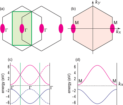
Figure 2. Brillouin zones and energy spectra of the four-band and two-band models of phosphorene. (a) The Brillouin zone is a rectangular in the four-band model, which is constructed from two copies of the hexagonal Brillouin zone of the two-band model. A magenta oval denotes a Dirac cone present at the  point. (b) The Brillouin zone is a hexagonal in the two-band model. A magenta oval denotes a Dirac cone present at the M point. (c) The band structure of the four-band model, which is constructed from two copies of that of the two-band model. (d) The band structure of the two-band model.
Download figure:
Standard image High-resolution image2.2. Two-band tight-binding model
We are able to reduce the four-band model to the two-band model due to the  point group invariance. We focus on a blue point (atom in upper layer) and view other lattice points in the crystal structure (figure 1). We also focus on a red point (atom in lower layer) and view other lattice points. As far as the transfer energy is concerned, the two views are identical. Namely, we may ignore the color of each point. Hence, instead of the unit cell containing four points, it is enough to consider the unit cell containing only two points. This reduction makes our analytical study considerably simple.
The two-band model is given by  with
with

The rectangular Brillouin zone of the four-band model is constructed by folding the hexagonal Brillouin zone of the two-band model, as illustrated in figure 2(a).
The equivalence between the two models (2) and (4) is verified as follows. We have explicitly shown the energy spectra of the four-band model (2) and the two-band model (4) in figures 2(c) and (d), respectively. It is demonstrated that the energy spectrum of the four-band model is constructed from that of the two-band model: The two bands are precisely common between the two models, while the extra two bands in the four-band model are obtained simply by shifting the two bands of the two-band model, as dictated by the folding of the Brillouin zone.
By diagonalizing the Hamiltonian, the energy spectrum reads

The band gap is given by

The asymmetry between the positive and negative energies arises from the  term.
term.
2.3. Low-energy theory
In the vicinity of the  point, we make a Tayler expansion of fi in (3) and obtain


The Hamiltonian (4) reads

with the Pauli matrices  , where

Hence, the dispersion is linear in the ky direction, but parabolic in the ky direction. The energy spectrum is given by

with

The low-energy Hamiltonian agrees with the previous result [30] with a rotation of the Pauli matrices  and
and  .
.
3. Phosphorene nanoribbons
We investigate the band structure of a phosphorene nanoribbon placed along the y direction (figure 1). There are two ways of cutting a honeycomb lattice along the y direction, yielding a zigzag edge and a beard edge. Accordingly, there are three types of nanoribbons, whose edges are (a) both zigzag, (b) zigzag and beard, (c) both beard. We show their band structures in figures 3(a), (b) and (c), respectively.

Figure 3. Band structure of phosphorene nanoribbons when the transfer energy t4 is nonzero and zero. (a, d) Both edges are zigzag. (b, e) One edge is zigzag and the other edge is beard. (c, f) Both edges are beard. The quasi-flat edge mode emerges for (a) and (b). When we set  , the quasi-flat band becomes perfectly the flat band. Flat and quasi-flat edge states are marked in magenta.
Download figure:
Standard image High-resolution image3.1. Quasi-flat bands
A prominent feature of a phosphorene nanoribbon is the presence of the quasi-flat edge modes isolated from the bulk modes found in figures 3(a) and (b). They are doubly degenerate for a zigzag–zigzag nanoribbon, and nondegenerate for a zigzag-beard nanoribbon, while they are absent in a beard–beard nanoribbon [figure 3(c)].
We explore the mechanism of how such an isolated quasi-flat band emerges in phosphorene. As far as the energy spectrum is concerned, instead of  as defined by (4), it is enough to analyze the two-band Hamiltonian

The term  only shifts the energy spectrum. The energy spectrum of
  is symmetric between the positive and negative energy spectra, as we have noticed in (5). We show the band structures of the three types of nanoribbons in figures 3(d), (e) and (f) for the Hamiltonian
  , where the quasi-flat edge modes are found to become perfectly flat.
It is a good approximation to set  , since the transfer energies t1 and t2 are much larger than the others. Indeed, we have checked numerically that almost no difference is induced by this approximation. The two-band model
  is well approximated by the anisotropic honeycomb model,

This Hamiltonian has been studied in the context of strained graphene and optical lattice [31–34]. The energy spectrum reads

which implies the existence of two Dirac cones at  and
and  with
with

for  , where we have set
  .
.
3.2. Flat bands in anisotropic honeycomb lattice
We explore the origin of the flat band in the anisotropic honeycomb-lattice model (13). It is instructive to study the change of the band structure of nanoribbon by changing the parameter t2 continuously, with  being fixed. We show the band structure with (a) the zigzag–zigzag edges, (b) the zigzag-beard edges, and (c) the beard–beard edges in figure 4 for typical values of t1 and t2.
- (i)
- (ii)
- (iii)
- (iv)For
 , the bulk band shifts away from the Fermi level, as follows from (14 ). The flat band is disconnected from the bulk band for the zigzag–zigzag nanoribbon and the zigzag-beard nanoribbon, where it extends over all of the region . On the other hand, the edge band becomes a part of the bulk band and disappears from the Fermi level for the beard–beard nanoribbon. See figures 4(j)–(l).


Figure 4. Band structure of anisotropic honeycomb nanoribbons. The flat edge states are marked in magenta. We have set  and
and  . We have also set (a, b, c)
  , (d, e, f)
  , (g, h, i)
  , (j, k, l)
  . The unit cell contains 144 atoms.
Download figure:
Standard image High-resolution image3.3. Topological origin of flat bands
The topological origin of the flat band has been discussed in graphene [29]. It is straightforward to apply the reasoning to the anisotropic honeycomb-lattice model (13). We consider one-dimensional (1D) Hamiltonian  in the kx space, which is essentially given by the two-band model (13) at a fixed value of
  . We analyze the topological property of this 1D Hamiltonian. Because the kx space is a circle due to the periodic condition, the homotopy class is
  .
.
We write the Hamiltonian as

It is important to remark that the gauge degree of freedom is present in this Hamiltonian [35]. Indeed the phase of the term  is irrelevant for the energy spectrum of the bulk system. However, this is not the case for the analysis of a nanoribbon, since the way of taking the unit cell is inherent to the type of nanoribbon, as illustrated in figure 5. It is necessary to make a gauge fixing so that the hopping between the two atoms in the unit cell becomes real, namely, t1 for the zigzag edge and t2 for the beard edge.

Figure 5. Unit cells and winding numbers for the zigzag and beard edges. It is necessary to make a gauge fixing in the Hamiltonian so that the hopping between the two atoms in the unit cell becomes real, namely, (a) t1 for the zigzag edge and (b) t2 for the beard edge. (c, d) The winding number reads  if the loop encircles the origin (red circle), and
  if not (blue circle). The origin is represented by a dot, where the Hamiltonian is ill defined.
Download figure:
Standard image High-resolution imageFor the zigzag edge we thus make the gauge fixing such that

where the parameter k corresponds to the momentum of zigzag nanoribbons. Here, t1 for the link in the unit cell and  for the neighboring link [figure 5(a)]. The topological number of the 1D system is given by

By an explicit evaluation,  is found to take only two values;
  for
for  , and
, and  for
for  . We may interpret this as the winding number as follows. We consider the complex plane for
 ![${{F}_{k}}({{k}_{x}})=|{{F}_{k}}({{k}_{x}})|{\rm exp} [i{{\Theta }_{k}}({{k}_{x}})]$](https://content.cld.iop.org/journals/1367-2630/16/11/115004/revision1/njp502867ieqn61.gif) . The quantity
. The quantity  counts how many times the complex number
  winds around the origin as
  moves from 0 to
  for a fixed value of k. Note that the origin implies
  , where the Hamiltonian is ill defined. We have shown such a loop for typical values of k in figure 5(b), where the horizontal axis is for Re
 ![$[{{F}_{k}}({{k}_{x}})]$](https://content.cld.iop.org/journals/1367-2630/16/11/115004/revision1/njp502867ieqn67.gif) and the vertical axis is for Im
and the vertical axis is for Im ![$[{{F}_{k}}({{k}_{x}})]$](https://content.cld.iop.org/journals/1367-2630/16/11/115004/revision1/njp502867ieqn68.gif) ,
,


The loop surrounds the origin and  when
when  and
and  , while it does not and
  when
when  : The loop touches the origin when
  . We have demonstrated that the system is topological for
  and trivial for
  .
.
We next appeal to the bulk-edge correspondence to the topological system. When we cut the bulk along the y direction, the 1D system has an edge. Since the edge separates a topological insulator and the trivial state (i.e., the vacuum state), the gap must close at the edge, namely, there must appear a gapless edge mode. The gapless edge mode appears for all  , implying the emergence of a flat band connecting the two Dirac points given by (15).
For the beard edge, we make the gauge fixing such that

and carry out an analogous argument (see figure 5). We reach at the conclusion that a flat band appears for  and connects the two Dirac points given by (15) but in an opposite way to the case of the zigzag edge.
3.4. Wave function and energy spectrum of edge states
We have explained how the flat band appears in the anisotropic honeycomb-lattice model. The flat band corresponds to the quasi-flat band in the original Hamiltonian  .
.
We construct an analytic form of the wave function at the zero-energy state in the anisotropic honeycomb-lattice model (13) as follows. We label the wave function of the atom on the outer most cite as ψ1, and that of the atom next to it as ψ2, and as so on. The total wave function is  if there are N atoms across the nanoribbon. The Hamiltonian is explicitly written as

with  . The eigenvalue problem
  is easily solved [36], yielding
  and
and ![${{\psi }_{2n+1}}={{[{{t}_{1}}(1+{{e}^{iak}})/{{t}_{2}}]}^{n}}{{\psi }_{1}}$](https://content.cld.iop.org/journals/1367-2630/16/11/115004/revision1/njp502867ieqn84.gif) . By solving the Hamiltonian matrix recursively from the outer most cite, we obtain the analytic form of the local density of states of the wave function for odd cite j,
. By solving the Hamiltonian matrix recursively from the outer most cite, we obtain the analytic form of the local density of states of the wave function for odd cite j,

with  . The wave function is zero for even cite. It is perfectly localized at the outermost site when
  , and describes the flat band.
We can derive the energy spectrum of the quasi-flat band perturbatively. With the use of this wave function, the energy spectrum  of the quasi-flat band is estimated perturbatively by taking the expectation value of the t4 term as

where  . On the other hand, we numerically obtain
  eV. The agreement is excellent.
4. Nanoribbons with in-plane electric field
It is possible to make a significant change of the quasi-flat edge band by applying external electric field parallel to the phosphorene sheet as in the case of graphene nanoribbon [4]. Let us apply electric field Ex into the x direction of a nanoribbon with zigzag–zigzag edges. A large potential difference ( ) is possible between the two edges if the width W of the nanoribbon is large enough. This potential difference resolves the degeneracy of the two edge modes, shifting one edge mode upwardly and the other downwardly without changing their shapes. We present the resultant band structures in figure 6 for typical values of Ex.

Figure 6. Band structure and conductance in unit of  of phosphorene nanoribbons with the both edges being zigzag in the presence of in-plane electric field Ex. (a, b)
  , (c, d)
  meV/nm, (e, f)
  meV/nm, (g, h)
  meV/nm. Magenta curves represent the quasi-flat bands, while cyan lines represent the Fermi energy. The unit cell contains 144 atoms.
Download figure:
Standard image High-resolution image
The energy shift due to the in-plane electric field is given by

This is well approximated by  for wide nanoribbons.
Electric current may flow along the edge. We derive the conductance. In terms of single-particle Greenʼs functions, the low-bias conductance  at the Fermi energy E is given by [37]

where ![${{\Gamma }_{{\rm R}({\rm L})}}(E)=i[{{\Sigma }_{{\rm R}({\rm L})}}(E)-\Sigma _{{\rm R}({\rm L})}^{\dagger }(E)]$](https://content.cld.iop.org/journals/1367-2630/16/11/115004/revision1/njp502867ieqn98.gif) with the self-energies
with the self-energies  and
and  , and
, and

with the Hamiltonian  for the device region. The self-energy
  describes the effect of the electrode on the electronic structure of the device, whose the real part results in a shift of the device levels, whereas the imaginary part provides a life time. It is to be calculated numerically [38–41].
We use this formula to derive the conductance,

where  is the step function
  for
for  and
and  for
for  . We show the conductance in figure 6. Without in-plane electric field, the conductance at the Fermi energy is
  since there is a two-fold degenerate quasi-flat band. Above the critical electric field, the conductance becomes 0 since the quasi-flat band splits perfectly. The critical electric field is determined as

The critical electric field is anti-proportional to the width W. This acts as a field-effect transistor driven by in-plane electric field.
5. Conclusion
We have analyzed the band structure of phosphorene nanoribbons based on the tight-binding model, and demonstrated the presence of quasi-flat edge modes entirely detached from the bulk band. We have shown the topological origin of the flat band in the anisotropic honeycomb-lattice (13) or, equivalently m the quasi-flat band in the original two-band model (4). The flat band bends because it is simply sifted by the transfer energy ( ) dependent of the momentum k and becomes a quasi-flat band. The energy spectrum is given by (22) in the lowest order of perturbation.
Acknowledgements
The author is very much grateful to N. Nagaosa and A.-L. Phaneuf-lʼheureux for many helpful discussions on the subject. He thanks the support by the Grants-in-Aid for Scientific Research from the Ministry of Education, Science, Sports and Culture No. 25400317.