


Abstract
We study optical back-action effects associated with confined electromagnetic modes in silicon nanowire resonators interacting with a laser beam used for interferometric read-out of the nanowire vibrations. Our analysis describes the resonance frequency shift produced in the nanowires by two different mechanisms: the temperature dependence of the nanowire's Young's modulus and the effect of radiation pressure. We find different regimes in which each effect dominates depending on the nanowire morphology and dimensions, resulting in either positive or negative frequency shifts. Our results also show that in some cases bolometric and radiation pressure effects can have opposite contributions so that their overall effect is greatly reduced. We conclude that Si nanowire resonators can be engineered for harnessing back-action effects for either optimizing frequency stability or exploiting dynamic phenomena such as parametric amplification.
Export citation and abstract BibTeX RIS

Content from this work may be used under the terms of the Creative Commons Attribution-NonCommercial-ShareAlike 3.0 licence. Any further distribution of this work must maintain attribution to the author(s) and the title of the work, journal citation and DOI.
1. Introduction
1.1. Historical review
Si nanowires (NWs) obtained by bottom-up synthesis offer unique properties to be exploited as device functionalities or to be explored as novel concepts in nanomechanics [1, 2]. In particular, the vapor–liquid–solid (VLS) growth mechanism allows to produce horizontally assembled Si NWs with control over their length and diameter and epitaxial single or double clamps [3–5]. The almost defect-free structural quality, unique surface smoothness and robustness of the clamping points have been found to result in NW-based resonators with exceptional dynamical parameters, such as resonance frequencies in the very high frequency range (30–300 MHz) and quality factors above 104. Nevertheless, the development of either practical device applications or systematic fundamental studies based on NW resonators carries along further challenges than NW growth control. In particular, the transduction of the NW vibration into a read-out signal is an issue of increasing difficulty as the NW dimensions are reduced in the quest for extreme device characteristics or unexplored physical phenomena. Optical transduction methods are receiving increasing interest over electrical methods mainly because of their high sensitivity, in the range of 1 pm Hz−1/2, allowing the detection of the thermomechanical vibrations of the NW resonators [6–10]. Moreover, optical transduction methods provide a non-invasive and highly versatile read-out scheme that can be employed in a wide variety of environments such as buffer solutions, ionic gases or high vacuum [11].
Over the last decade, it was believed that when device dimensions are shrunk beyond the optical wavelength, strong diffraction effects emerge and optical read-out methods would lose their high sensitivity. However, recent works have overcome this limitation by coupling the resonator to optical microcavities or by coupling the evanescent field of the confined light in the semiconductor structure (usually called whispering gallery modes or Mie modes) to a standing wave sustained by the incident and the reflected laser beam focused on the structure [12, 13]. In particular, laser beam interferometric read-out has been demonstrated as a highly sensitive transduction method for the characterization of the mechanical resonances of Si NWs and for testing their performance as nanomechanical sensors. Besides its high sensitivity for detecting the vibrations of nanomechanical resonators, optical transduction methods have been demonstrated to produce a feedback force on the resonator that induces variations in the resonance frequency [14–16]. In the case of Si NW resonators, there are mainly two different back-action effects that can be expected from the interaction with an external optical field: the bolometric effects and the radiation pressure exerted on the resonator. The bolometric effect comprises the so-called thermo-optics effects in which, at this wavelength, the most important one is the dependence of Young's modulus on temperature. In contrast, radiation pressure effects have recently been reported in such tiny structures, being the primary force used in cooling experiments pursuing the quantum regime [17].
1.2. Motivation
In this work, we analyze the consequences of optical back-action effects in Si NW resonators as a function of the resonator geometrical dimensions. We present experimental evidence for the shifting of the fundamental resonance frequency of the resonators when the laser power is varied. Depending on the measured NW, the frequency shift can be positive or negative. Then, we present a theoretical model that considers both the temperature dependence of the Young's modulus of NWs and the effect of the radiation pressure in the calculus of the effective force acting on the resonator. Finite element simulations based on this model allow us to conclude that there are two different regimes in which each effect dominates over the other one, depending on the NW geometrical dimensions. For the same length, radiation pressure dominates for NWs with smaller diameter, while the temperature dependence of Young's modulus dominates for thicker NWs. The presence of back-action effects in NW resonators has important implications for device applications and performance optimization, which are discussed in the final section.
2. Experimental results
2.1. Sample preparation
The measurements presented in this work were performed on silicon NWs grown horizontally by the VLS mechanism in a chemical vapor deposition chamber at the sidewalls of prepatterned microtrenches (figures 1(a) and (b)). We selected singly clamped NWs grown normal to the trench sidewall where they were anchored. Their lengths range from 8 to 14 μm and their diameters from 80 to 250 nm, resulting in effective masses of 50–1000 fg. The distance between the NW and the substrate lies in the 1000–2000 nm range. According to previous results reported in the literature, the NW symmetry is broken in the fabrication process; therefore, each flexural vibration mode is split into two close resonance peaks of similar amplitudes consisting of the NW vibrating in two orthogonal planes [1, 18]. Hereinafter, to discern the two first flexural modes, we will refer to as slow mode (s-mode) the one with the lower frequency; and as fast mode (f-mode) the one with the higher frequency.
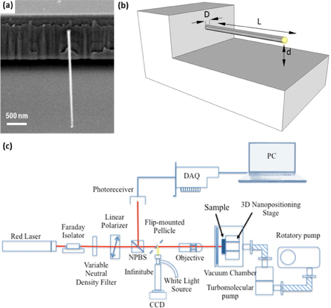
Figure 1. Experimental setup. (a) Scanning electron microscopy image of a singly clamped NW horizontally grown at the vertical sidewall of a step-like microstructure. (b) Schematic drawing showing the most relevant NW parameters. (c) Experimental read-out setup based on a homemade interferometer system; the incident beam is focused on the sample by means of a long working distance objective, analyzed by passing through a non-polarized beam splitter (NPBS) and collected by a photoreceiver.
Download figure:
Standard image2.2. Measurement setup
The experimental measurements of the NW oscillation were made using a homemade interferometric system (figure 1(c)) with a He–Ne laser (20 mW, 633 nm; Thorlabs). The optical power of the incident beam on the NWs was controlled with a variable filter ranging from 10 to 500 μW. The laser beam is focused on the NW by means of a long working distance Mitutoyo objective (50×) that reaches a spot size of about 2 μm. The sample containing NWs was placed in a high vacuum chamber (10−7 mbar), which is pumped down by using a rotatory and a turbomolecular pump (Leybold). In order to avoid backscattering reflections that could cause laser damage, a Faraday isolator cell has been introduced within the light path. Following the current trends in the field claiming the maximum displacement sensitivity, the laser beam is intentionally linearly polarized in such a way that the electric field is contained in the same plane as the silicon NW [7]. A collimated LED white source is used to image the laser spot on the chip by means of a CCD camera. The position of the chip is controlled by a three-dimensional nanopositioning stage (Attocube).
2.3. Description of measurements
We made measurements of the mechanical resonance of more than 20 NWs as a function of the incident power. The mechanical quality factors of the peak resonances are of about 3000, being the same for the s-mode and the f-mode owing to the high degree of axial symmetry they present. Figures 2(a) and (b) show the spectra of two representative examples of NWs for increasing laser power ranging from 10 to 500 μW. These results have been reproducible in all the observed NWs. The resonance frequencies of both modes of the NW of figure 2(a) are shifted to lower values as the power increases, while the opposite behavior is observed for the case shown in figure 2(b). Figure 2(c) shows the changes in resonance frequencies for these two NWs as a function of the incident power. Each point in this graph is the result of the average of 100 independent measurements. The NW that experiences the negative frequency shift has a length of 12.7 μm and a diameter of 165 nm, and the average sensitivity of the frequency shift to increasing power for the s- and f-modes is −8.4 × 10⁻⁶% μW−1, as obtained from linear fitting of the experimental data. The NW with positive shift has a length of 9.3 μm and a diameter of 90 nm, and the average sensitivity of the frequency shift to increasing power for the s- and f-modes is 27 × 10−6% μW−1. The lack of symmetry in the obtained results for both NWs strongly suggests that different back-action mechanisms may be dominating in each case.
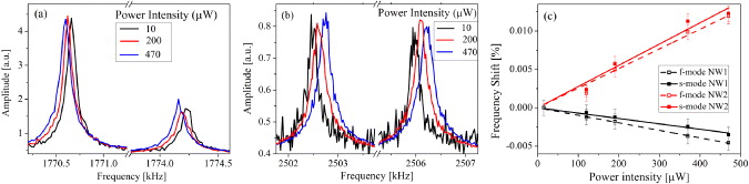
Figure 2. Back-action measurements. (a) A representative example of a thermomechanical noise spectrum measurement for different laser beam power intensities for a NW with resonance frequencies of the s- and f-modes that decrease for increasing power (L = 12.7 μm; d = 165 nm). (b) A representative example of a thermomechanical noise spectrum measurement for different laser beam power intensities for a NW with resonance frequencies of the s- and f-modes that increase for increasing power (L = 9.3 μm; d = 90 nm). (c) Resonant frequencies of each mode for both NWs as a function of the power intensity; linear fittings provide values for the sensitivity of the relative frequency shifts (%) with different power of −9.8 × 10⁻⁶% μW−1 (NW1, f-mode), −7.0 × 10⁻⁶% μW−1 (NW1, s-mode), 26 × 10−6% μW−1 (NW2, f-mode) and 28 × 10−6% μW−1 (NW2, s-mode).
Download figure:
Standard image3. Theoretical analysis
3.1. Equation of motion
Without loss of generality, we can use the Galerkin decomposition of the modes in the resonator and solve the equation of motion for a lumped harmonic oscillator for each mode:

where meff , γeff and keff , respectively, are the effectives mass, damping and stiffness of the first flexural mode of the NW, Fth is the thermomechanical force that sustains its movement and F' is an additional force acting on the resonator. This equation is valid for each mode; therefore, we can treat the f- and s-modes independently. On the one hand, the absorbed optical power heats up the NW. The inversely proportional temperature dependence of the Young's modulus of the material leads to variation of the effective resonator stiffness, which shifts the resonance to lower frequencies. On the other hand, it is a known fact that the radiation pressure is a position-dependent force and, therefore, it can be viewed as a change in the effective spring constant and written as a Taylor series, which at first order is expressed as  , where F0 is a static contribution that can be neglected because it does not produce any significant effect on the resonance frequency. Taking into account that the low finesse of our cavity does not introduce any delay between the acting force and the resonator displacement, which means that the force is real, we finally obtain the modified harmonic oscillator equation

where Teff is the first mode effective temperature as defined below. As we can see in this expression, the contribution of temperature will shift the resonances of the oscillators to lower frequencies because the temperature gradient is always positive, while the radiation pressure effect can induce a shift either negative or positive because, as we will see below, the force gradient varies from positive to negative as a function of geometrical parameters.
3.2. Electric field calculations
The existence of previous studies on the geometrical confinement of electromagnetic modes in SiNWs strongly leads us to an exhaustive analysis of the effect of the dimensions and the distance to the substrate of the resonators [13]. To obtain the power absorbed by the NW and the radiation pressure force, we solve Maxwell's equations by using a finite element method (FEM) commercial package, COMSOL Multiphysics5. For the sake of simplicity, the experimental device introduced in the main text will be modeled as an ideal infinite cylinder suspended above a substrate. Since the wavelength is significantly larger than the NW transversal characteristic size, we can neglect the shape details of the cross-section. Therefore, although the actual cross-section of the experimental NW is hexagonal, a cylindrical structure is a good approximation. By harnessing the device symmetries, it is possible to address the three-dimensional problem by targeting the two-dimensional cross-section, thereby simplifying its solution and decreasing the computational cost. The simulation region and the substrate thickness are about 50 and 20 times the cylinder diameter, respectively. Both elements were dimensioned to minimize its influence on the final electric field distribution. The simulation region is surrounded by a perfectly matching layer boundary region to accurately describe the open boundary. The laser beam is described as a Gaussian beam of waist w0 and wavelength λ and is focused on the NW's center [19]. The polarization is chosen in such a way that the electric field is parallel to the cylinder axis (TE polarization). FEM simulations have been performed at 633 nm wavelength with a beam waist of 2 μm. The values used for the real and imaginary parts of permittivity for silicon and gold are [20]: εSi = 15.1 + i0.165 and εAu = −10.7 + i0.9.
3.3. Bolometric effect
The power absorbed by a physical system is calculated by using the scattered electric field and the imaginary part of its permittivity [21]:

where ω is the optical angular frequency, E is the electric field and ε is the system's permittivity. As shown in figure 3(a), the power absorbed by the NW depends on both the diameter and the distance between the NW and the substrate. The diameter dependence is related to the distribution of the confined electromagnetic modes inside the semiconductor structures, while the distance dependence is related to the coupling between these modes and the standing wave that arises from the interference between the incident and the reflected beam from the substrate. Note that the percentage of power absorbed is plotted in log scale. The first Mie mode absorbs about 1% of the incident power, while the third confined electromagnetic mode about 20%, having approximately the same efficacy section. Moreover, the different electromagnetic field distribution of the Mie modes produces changes in the localization of maxima and minima of optical power absorption in the standing wave field.
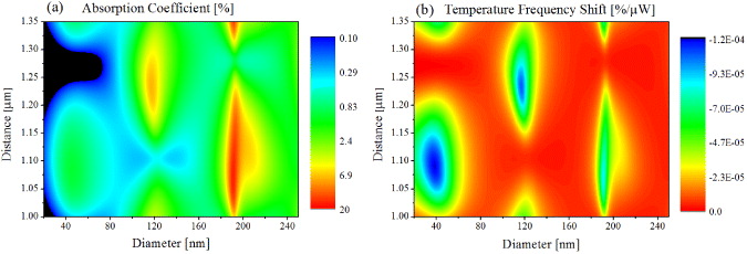
Figure 3. Calculation of bolometric back-action effects. (a) Absorbed optical power (%) in an NW of 1 μm length focusing a beam of 100 μW and a width of 2 μm in the middle of the NW at 1 μm from its free end, as a function of the NW diameter and the distance to substrate. (b) Relative frequency shift (divided by the incident optical power, in units of % μW−1) due to the temperature dependence of Young's modulus as a function of the NW diameter and the distance to the substrate.
Download figure:
Standard imageOnce we have the optical power absorbed we calculate the temperature distribution in the NW by applying the heat diffusion equation. We assume that the penetration depth of the absorbed power is several orders of magnitude larger than the NW typical thickness; therefore the temperature distribution along the x- and y-axis is constant, T = T(z) . We also neglect any eventual heat convective losses as well as irradiative power losses. The temperature distribution T(z) , determined with respect to a given background temperature, is finally derived by applying the one-dimensional heat diffusion equation

where A is the cross-sectional area, κe is the effective thermal conductivity and p(z) is the absorbed power density produced by the Gaussian laser beam that is described by

where Pabs is the total power absorbed, w0 is the beam waist and z0 is the laser spot coordinate along the NW axis. In order to mimic the experimental results, we set in the calculation w0 = 2 μm and z0 = (L − 1) μm, as we performed all the experiments focusing the laser close to the free end of the NW.
Besides, the geometry of the problem imposes the following boundary conditions:

which corresponds to zero heat flux at the free NW end and

which is equivalent to considering a null increment of temperature at the clamping region. FEM calculations also confirm this assumption (data not shown).
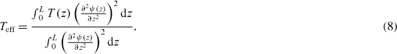
By using the calculated temperature distribution along the NW, we calculate the equivalent effective temperature for the first flexural mode taking into account the Rayleigh method
This effective temperature allows us to directly obtain the resonance frequency shift by applying

where ωn is the initial angular frequency of the first resonant mode and b is the temperature coefficient of Young's modulus, which for silicon is b = 5.2 × 10 − 5 K−1. Figure 3(b) shows the relative frequency shift per incident optical power unit, due to the Young's modulus' temperature dependence induced by a beam focused at the free end of a 10 μm long NW, as a function of its diameter and distance to the substrate. Particular combinations of the NW diameter and the distance to the substrate produce maxima of power absorption and thus frequency shift. Then, the effective temperature is proportional to the length and is inversely proportional to the diameter squared, Teff ∝L/d2 . Comparing the absorbed optical power and the resonance frequency shift, we found that besides the fact that the lower Mie mode indexes absorb less optical power, the resonance frequencies are more affected in these NWs because there occurs a higher increment of temperature due to the reduction of the effective thermal conductivity because of its small cross-section. Of course, the effective temperature is positive so the bolometric effect always lowers the resonance frequency of our devices.
3.4. Radiation pressure
On the other hand, the radiation pressure on the silicon NWs can be calculated by means of the asymmetries of the Maxwell stress tensor. This requires knowledge of the scattered electric E(z,y) and magnetic H(z,y) fields, which are also performed by using the FEM software package. The net force acting on a closed domain can be computed by integrating the Maxwell's stress tensor over a close path

where

 is a unit vector normal to the integration path pointing outwards and μ is the permeability. The electric and magnetic fields are those obtained by solving Maxwell's equations. As has been stated before, the distance dependence of the optical force induces a frequency shift that is proportional to the gradient of the radiation pressure and inversely proportional to the effective stiffness, that is, proportional to the length cubed and inversely proportional to the diameter to the fourth power because keff ∝d4 /L3 :

We plot this gradient as a function of both the distance between the SiNW and the substrate and its diameter in figure 4(a), while the computed relative frequency shifts associated with this force are displayed in figure 4(b), assuming a length of 10 μm. Note that the exerted radiation pressure is larger for the narrowest NWs, with diameters around 40 nm, that support the first Mie resonance; therefore, they present a higher force gradient. These NWs are also the ones with lower spring constant, so when we analyze the frequency shifts induced by this force, this is clearly enhanced in the thinner NWs. Besides, we observe different regions in which the sign of the gradient changes from positive to negative, depending again on the diameter as well as on the distance to the substrate. In this way, radiation pressure can produce both effects shifting the resonance of our devices to higher or lower frequencies depending on the geometrical parameters. As in the case of power absorption, the force gradient depends periodically on the distance to the substrate having a period of λ/2.
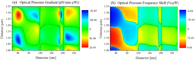
Figure 4. Calculation of radiation pressure back-action effects. (a) Force gradient per incident optical power (expressed in units of pN (μW nm)−1) produced on an NW of 10 μm length focusing a beam of 100 μW and a beam waist of 2 μm centered on the NW at 1 mm from its free end, as a function of the NW diameter and the distance to the substrate. The sign of the gradient force changes from positive to negative depending on the diameter and the position of the NW. The highest values of force gradient are achieved around the first Mie mode. (b) Relative frequency shift per incident optical power unit (in units of % μW−1) produced by the optical beam due to the radiation pressure effects as a function of the NW diameter and the distance to the substrate. Radiation pressure effects clearly become more important as the diameter decreases.
Download figure:
Standard image3.5. Combined effect for different lengths
So far we have considered a NW with a length of 10 μm. It is important to note that although the relative percentages of optical absorption as well as the radiation pressure calculation are independent of the device length, the final resonance frequency shift calculation has taken into account the actual geometry of the device. To further state the regimes in which the radiation pressure dominates over the bolometric force, we perform the calculation by varying the length of the devices. Figure 5 shows the total induced frequency shifts due to both effects for different NW lengths. Short NWs, of lengths smaller than 5 μm, will be affected mainly by bolometric effects decreasing the resonance frequency of the devices, whereas the resonance shift of thin Si NWs, with a diameter smaller than 90 nm, will be dominated by the radiation pressure. As the bolometric effect is proportional to the length while the radiation pressure effect is proportional to the length cubed, when the length of the NW is increased the effect of radiation pressure begins to dominate in a wider range; for example, for NWs of 20 μm length, the radiation pressure is the predominant frequency shifting effect for NWs with diameters up to 250 nm. These conclusions are consistent with our experimental results, as we presented a thick NW showing negative frequency shift, probably due to the bolometric effect, while the thinnest one presents a positive frequency shift that can only be produced by the radiation pressure effect.
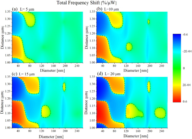
Figure 5. Relative frequency shift per incident optical power (% μW−1) produced by the combined contributions of bolometric and radiation pressure effects as a function of the NW diameter and the distance to the substrate for different lengths: (a) L = 5 μm, (b) L = 10 μm, (c) L = 15 μm and (d) L = 20 μm.
Download figure:
Standard image4. Analysis and implications of the results
Remarkably, for some NWs both contributions, bolometric effects and radiation pressure, can have opposite signs that cancel their contributions. Hence, it is possible to find cases where the resonance frequency remains almost unaltered by the laser beam. This is a significant finding owing to its implications for device performance in terms of frequency stability, because laser intensity fluctuations and phase noise will be translated into mechanical frequency fluctuations via the optomechanical coupling effects described above. As a consequence, NW s where back-action effects are balanced are of interest whenever a high frequency stability is desired, which includes device applications such as nanomechanical sensing or signal processing. Conversely, optical back-action can turn out to be a relevant advantage in applications consisting of active signal filtering [22–24], postfabrication tuning of the mechanical properties [25–28] or even to induce optomechanical coupling [29–31]. It is a known fact that it is possible to produce parametric amplification by inducing a change in the resonator spring constant at twice the resonance frequency [32, 33]. In our experimental setup, there appears an intrinsic dependence of the optical back-action and therefore the modulation of the resonator spring constant on its position with respect to the substrate, that is, its movement, due to its interaction with the standing wave [13]. This suggests that it is possible to design devices in which the optomechanical feedback gain is strong enough to produce intrinsically parametric amplification or cooling in the resonator and then, respectively, enhance the sensitivity of the devices or allow the study of quantum effects in mesoscopic systems [34, 35].
5. Conclusions
To conclude, we have demonstrated that interferometric laser beam read-out exerts a measurable effect on the resonance frequency of silicon NW resonators. This effect can be split into two different mechanisms: the temperature dependence of Young's modulus, or bolometric force, and the radiation pressure. The thermal effect is prevalent in long and wide NWs and always shifts the resonance to lower frequencies, as the resonator material becomes softer through the dependence of Young's modulus on the temperature. When the diameter of the resonator decreases, the radiation pressure becomes more and more important, shifting the resonance to either lower or higher frequencies depending on the relative NW–substrate distance and the particular confined electromagnetic mode distribution. Our study has shown that optical back-action can be enhanced or suppressed by proper device parameter engineering.
Acknowledgments
The authors acknowledge financial support from the Spanish Science Ministry through projects TEC2009-14517-C02-01/02, TEC2008-06756-C03-01 and CSD2010-00024 and from the EU through the project ERC-Starting Grants-StG-2011-278860-NANOFORCELLS. DR acknowledges financial support from the EU grant IOF-2009-254996.