


Abstract
The spin structure of quantum well states (QWSs) in three-monolayer-thick gold overlayers on W(110) and Mo(110) is studied experimentally by spin- and angle-resolved photoelectron spectroscopy and theoretically by ab initio calculations. The spin–orbit coupling effects manifest themselves differently in the spin structure of atomic-like d and delocalized sp QWSs depending on how strongly the states are influenced by the substrate. The QWSs of a d character show a strong spin polarization with an almost identical structure for W(110) and Mo(110), suggesting a weak interaction with the substrate, whereas for sp QWSs, the interaction is much stronger, which to a large extent determines their splitting and spin polarization. The theoretical model yields a qualitative agreement with the experiment and explains the observed behavior.
Export citation and abstract BibTeX RIS

Content from this work may be used under the terms of the Creative Commons Attribution 3.0 licence. Any further distribution of this work must maintain attribution to the author(s) and the title of the work, journal citation and DOI.
GENERAL SCIENTIFIC SUMMARY Introduction and background. Quantum well states form a two-dimensional (2D) electronic system in thin overlayers at surfaces of many metals and semiconductors. They can carry current parallel to the surface without producing a current in the bulk. An important direction in the emerging field of spintronics is to make the 2D states carry spin current. Surfaces of nonmagnetic materials are especially interesting in this respect due to the idea of manipulating the spin structure by electric rather than magnetic field. This possibility is opened up by the spin–orbit splitting of 2D states, known as the Rashba effect.
Main results. We study the spin structure of quantum well states in thin gold overlayers on (110) surfaces of tungsten and molybdenum by spin- and angle-resolved photoelectron spectroscopy. We have found the effect of the substrate on the splitting to be weak for atomic-like d states and strong for delocalized sp states, where it affects both the energy splitting and the degree of spin polarization. The experimental results are interpreted using ab initio electronic structure.
Wider implications. Detailed knowledge of how the Rashba splitting and polarization depend on the properties of the surface, especially the understanding of the role of the substrate, is instrumental in designing spintronic devices. This paper contributes to the insight into the fundamental mechanisms of the interaction of 2D states at the surfaces with the underlying substrate.
 Figure. Experimental angle- and spin-resolved photoemission spectra for three monolayers of Au on W(110)—(a) and Mo(110)—(c) along the
  direction in the Brillouin zone in comparison with theoretical calculations of the spin density of states for the same systems—(b), (d), accordingly. The two sets of the arrows point to the differences between the two systems. The spectra for opposite spin directions are shown by red and blue lines. The corresponding spin–orbit splitting is indicated by the vertical red and blue bars.
1. Introduction
The spin structure of low-dimensional metallic systems caused by a strong spin–orbit coupling has attracted much attention in recent years because of a much larger spin–orbit splitting than in traditional semiconductors and larger spin currents that arise from the spin Hall effect [1–5]. The relativistic effects are essential for spintronics, as they facilitate the manipulation of the electron spin without magnetic fields. This makes it especially interesting and important to study the spin structure of a wide variety of low-dimensional metallic and non-magnetic systems.
In crystals with inversion symmetry, the bulk continuum states are doubly degenerate according to the Kramers theorem, but in a semi-infinite crystal the Kramers degeneracy is lifted and the surface states are spin–orbit split. This effect was first experimentally observed for the surface state on Au(111) single crystal [6] and later for a wide range of single-crystal surfaces and more complex two-dimensional (2D) systems [7–15]. A qualitative description of the spin–orbit splitting of the surface states is given by a simple Rashba–Bychkov (RB) model, originally developed for a 2D free-electron gas, in which only the potential gradient perpendicular to the surface is taken into account; a free-electron-like motion parallel to the crystal surface is assumed [16, 17]. The RB model yields a splitting of the parabolic dispersion along the surface-parallel momentum k∥ and the opposite spin polarization of the states with opposite k∥, as illustrated in figures 1(a) and (b). Here the spin–orbit splitting depends only on the surface-perpendicular potential gradient; it increases linearly with k∥, with the spin orientation being perpendicular both to k∥ and to the surface normal. The spin structure of the surface states on Au(111) observed in spin- and angle-resolved photoelectron spectroscopy (SARPES) experiments [18, 19] has been found to follow this prediction. Currently, a wide range of spin–orbit phenomena in 2D systems has been qualitatively understood in terms of the RB model.

Figure 1. Schematic presentation of the spin–orbit-induced spin structure of surface states and resonances: parallel momentum dispersion (a) and (c) and a sketch of spin-resolved photoelectron spectra (b) and (d). Red and blue colors indicate the opposite spin orientations. (a), (b) According to the RB model [16, 17] the free-electron parabola is split into two branches with opposite spin orientations shifted by k0 in the opposite directions. (c), (d) Antisymmetrically polarized surface resonances in the bulk continuum, according to Krasovskii and Chulkov [22].
Download figure:
Standard image High-resolution imageThe splitting of the surface states depends mainly on the atomic constituents of the material, as the larger atomic numbers lead to stronger potential gradients [19, 20]. In particular, the splitting of the surface states on Ag(111) was found to be much smaller than on Au(111) [19]. The RB effect was also observed in quantum well systems: in [28], it was shown that the spin structure of the sp-quantum well state (QWSs) in thin layers Ag and Au on W(110) is consistent with the RB model but, surprisingly, the energy splitting was found to be virtually the same for Ag and Au overlayers, in spite of their very different atomic numbers [25, 28]—contrary to the large difference between the (111) surfaces of Ag and Au single crystals [19]. Similar to the case of Ag and Au overlayers on W(110), the SARPES experiments on Au, Ag and Cu monolayers (MLs) on W(110) and Mo(110) [24, 25] showed that the spin–orbit splitting in these systems does not strongly depend on the atomic number of the adsorbate; for the lighter Ag and Cu elements, it is even larger than for Au. The spin–orbit splitting in these systems is determined by the substrate: for the molybdenum substrate, the splitting of the spin-polarized resonances in the MLs of the noble metals is much smaller than for the heavier tungsten [24, 25].
It has been recently shown [21–23] that the RB effect may also manifest itself as a surface-local spin polarization of bulk continuum states, as is schematically shown in figures 1(c) and (d). It arises from the spin-dependent reflection of the Bloch waves, incident from the interior of the crystal from the surface barrier. The interference of the two waves causes a beating of the net spin density, which decays into the depth of the crystal. The surface sensitive technique of photoemission can detect the surface polarization of the bulk states. Recently, this theory was applied to the analysis of the spin structure of the surface resonances on W(110) and its modification upon the deposition of an Al ML [23].
Thus, two aspects of the RB effect can be distinguished: (i) the energy splitting of the discrete states—surface states or QWSs—accompanied by the spin polarization; and (ii) the spin polarization of the continuum spectrum, where each state is doubly degenerate, i.e. the surface spin resonances. The question arises of how the two aspects manifest themselves in a thin film that supports QWSs. QWSs are expected to combine both scenarios, as, on the one hand, they are discrete states, while on the other hand, they are a precursor of the bulk band. An important question is the influence of the interface between the deposited layers and the substrate on their spin structure, as this may shed light on the material dependence of the size of the splitting; a related question is how the spin splitting and polarization depends on the orbital character and the spatial extent of the QWS wave functions.
This work aims at a comparative study of the spin structure of the QWSs of a d and sp character in three-layer Au films on W(110) and Mo(110) surfaces. The two substrates are isoelectronic and have very close geometry but very different atomic numbers, which enables us to reveal the contribution of the substrate to the spin structure of the QWSs and to study the difference between the delocalized sp and localized 5d states. The three-layer thick film perfectly suits this purpose because it is thin enough to feel the substrate and, at the same time, it is thick enough to energetically separate the QWSs of a d and sp character. Their very different behavior—rapidly dispersing with k∥ sp states and flat d bands—makes this system an ideal choice for an efficient SARPES analysis of the surface spin structure.
2. Experimental techniques
The experiments were carried out at Helmholtz–Zentrum Berlin (BESSY II) at beamline U125/2-SGM with linearly polarized light using the 'Phoibous' energy analyzer and the Mott spin detector operated at 26 keV with the in-plane spin orientation perpendicular to the emission plane. The angle of light incidence under normal emission was 55°. The base pressure in the experimental chamber during the experiment was on the level of 1–2 × 10⁻¹⁰ mbar. Part of the experiment was carried out at the Russian-German beamline at BESSY II and in the Resource Center of Saint-Petersburg State University 'Physical methods of surface investigation'. The W(110) and Mo(110) surfaces were cleaned by a standard procedure with preliminary oxidation of the surface at 1200 °C with subsequent flashing to 2000 and 1800 °C at a pressure below 5–7 × 10⁻¹⁰ mbar [23–28]. Layers of Au atoms with thickness of 3 ML were deposited by evaporation from pieces of Au melt-tipped on a thin W–Re wire. Deposition of Au on the W(110) and Mo(110) surfaces was carried out at room temperature. The thickness of the Au layers was calibrated by the energy location and the intensity of QWSs developed in Au films. The deposition was stopped when the QWS structures corresponding to the thickness of exactly 3 ML reached the maximal intensity [29]. Preliminary calibration of the flux of evaporated atoms was effected by the quartz microbalance method. The dispersion relations of electronic states for the systems with 3 ML of Au on W(110) and Mo(110) were measured by SAPRES in the  direction of the W(110) surface Brillouin zone with p-polarized light of the photon energy of 62 eV.
3. Computational methodology and notation
The ab initio calculations of the spin density distribution at the surface were carried out in a repeated slab geometry: the substrate was modeled by 17 atomic layers of Mo or W and three Au layers were put on both sides of the slab. The Au overlayer was chosen to have the lateral lattice of the (110) substrate, but the interlayer spacing was as in Au(111). The overlayer was chosen to have the ABC packing, which lowers symmetry of the overlayer relative to the substrate.
The ground-state electronic structure of the model system was calculated with the self-consistent (in the local density approximation (LDA)) full-potential linear augmented plane wave method [30]. The relativistic effects are included within the two-component approximation [31]. The theoretical analysis of the measured spectra in section 5 will be made in terms of the spin-resolved k∥-projected density-of-states (DOS) functions. Because the semi-infinite substrate is modeled by a finite slab, the k∥-resolved total DOS N(E,k∥) is defined as a sum over all (discrete) states λ with energy E and Bloch vector k∥:  , with the δ function being replaced (for the sake of presentation) by a Gaussian of a full width at half maximum γ = 0.25 eV. The basic quantity for the interpretation of the spin structure of surfaces is the spin- and depth-resolved k∥-projected DOS ρ↑(↓)k∥(z,E) defined as a sum of the densities of spin ↑ or ↓ (integrated over a surface parallel plane z = const, with r = (r∥,z)):

To reveal the real space origin of the observed spin polarization of the photocurrent, we introduce the partial net-spin spectral density S(E,k∥) defined as the integral of the net-spin density σk∥ = ρ↑k∥ − ρ↓k∥ over a certain z-interval in the slab, so that SAu(E,k∥) stands for the polarization of the Au overlayer and Stot(E,k∥) for the total spin polarization of the surface. The latter is obtained by integrating σk∥ from the middle of the slab to the middle of the vacuum region. (For the application to bulk continuum states, see [22].)
Because the actual atomic geometry of the Au overlayers is not known, the crystal structure assumed by this model is rather hypothetical. To get an idea of the range of the uncertainty introduced at this stage, we compared the structure of the QWSs in two isolated Au three-layer slabs: the one of this model and a three-layer with the Au(111) structure. The gross features of the QWS spectra were found to agree to a reasonable level, but the changes in the 5d band were of the order of several tenths of eV. At the same time, the QWSs of sp character were much more stable to the lateral geometry. Another difficulty with modeling the Au overlayer is a rather large error in the quasi-particle energies of Au 5d states introduced by the LDA. In [32], by comparison with optical measurements, the Au 5d band of the bulk crystal was found to be shifted by about 0.5 eV to lower energies relative to the LDA result. Nevertheless, our model yields the energy separation of d and sp states similar to the experiment; it is expected to provide a semi-quantitative description of the spin structure of the Au overlayers.
4. Experimental results
Figures 2(a) and (b) show the measured normal emission energy distribution curves (EDCs) of the valence band during the deposition of Au on W(110) and Mo(110) surfaces. In the course of the deposition, the substrate-related spectral features, in particular the surface resonance at around 1.3 eV, are seen to weaken and the peaks due to QWSs gradually emerge. Their energy location changes abruptly in coming from 1 to 2 and then 3 ML. For 1 ML, the characteristic peaks are at 3.3, 3.7 and 4.9 eV, for 2 ML they are at 2.7, 3.0 and 3.7 eV and for 3 ML, the most prominent are the peaks at 2.5 and 3.5 eV. A detailed analysis of the QWSs in thin Au layers on W(110) is given in [25, 29, 33]. The respective Au QWSs on Mo(110) are at 3.1 and 3.6 eV for 1 ML, 2.6 and 2.9 eV for 2 ML and 2.4 and 3.4 eV for 3 ML.
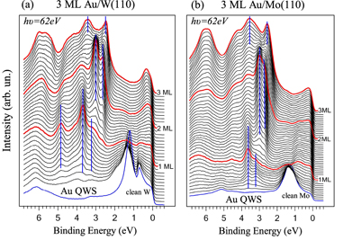
Figure 2. Angle-resolved normal emission EDCs under deposition of Au on W(110) (a) and Mo(110) (b) showing the changes of the QWSs developing in the Au film starting with submonolayer coverages and till the thickness of 3 ML was reached. The characteristic features of the QWSs for the thicknesses of 1, 2 and 3 ML of Au are marked by blue vertical lines. The photoemission spectra corresponding to 1, 2 and 3 full ML are shown by red lines.
Download figure:
Standard image High-resolution imageDuring the deposition, the peaks corresponding to the QWSs of a complete ML first gradually grow and then weaken as the next ML is forming. These structures are shown by blue bars in the figures and the spectra corresponding to the complete 1, 2 and 3 ML are given by red lines. The deposition was terminated when the structures characteristic of the 3 ML thickness reached the maximal intensity.
Figures 3(a) and (b) show for the 3 ML Au films on W(110) and Mo(110), respectively, the dispersion of the ARPES spectral features for k∥ along  . The atomic-like QWSs of 5d character are located below 2.5 eV binding energy; the rapidly dispersing sp states are observed over the interval from 2.5 eV to the Fermi level. Note that the surface-normal projected bulk band structure of W(110) and Mo(110) (along the ΓN line of the bulk BZ) has a gap between 6.3 and 3.3 eV [29, 33], which strongly reduces the interaction of the d states around
  with the substrate. At the same time, the sp states may interact with the valence band states of both substrates. This is seen in the energy–momentum maps of figure 3 as well-discernible wiggles in the parabolic features above 2.5 eV (indicated by red dashed lines). They are caused by the avoided-crossing behavior due to the interaction of the Au sp QWSs with W 6p and Mo 5p states (similar avoided-crossing effects have been earlier observed for sp QWSs of Ag on W(110) [34].)

Figure 3. Dispersion of sp- and d- QWSs measured by angle-resolved photoemission in the direction of the surface Brillouin zone for 3 ML of Au on W(110) (a) and on Mo(110) (b). Color map shows the second derivative of the EDCs with respect to energy. White color refers to negative values (spectral maximum) and black color to positive values (spectral minimum).
Download figure:
Standard image High-resolution imageAccording to the peak dispersion maps in figure 3, both sp and d QWSs behave nearly identically for the two substrates, save for a slight energy shift caused by the different energy location of the local forbidden gap in the band structure of the substrate. For a detailed analysis of this effect, see [33]. Figures 4(a) and (b) compare the spin- and angle-resolved photoelectron spectra of Au on W(110) and Mo(110), respectively, for binding energies above 3 eV. The values of k∥ of the measured spectra are indicated by white vertical lines in figure 3. The spin splitting of the spectral structures due to sp QWSs in Au/W(110) is clearly seen in figure 4(a): at k∥ = 0.6–0.8 Å−1, it is about 0.15–0.25 eV. In Au/Mo(110), the polarization and the splitting of the spectra is much smaller, see figure 4(b), which points to the influence of the spin–orbit coupling in the substrate: for the heavier tungsten atom it is much stronger. Interestingly, at k∥ = 0.75–0.77 Å−1, the spin-↑ peak in Au/W(110) appears at a larger binding energy than its spin-↓ counterpart, whereas in Au/Mo(110), the energy sequence of the corresponding structures is the opposite. We will demonstrate by the theoretical analysis in section 5.2 (figures 9 and 10) that this behavior is a consequence of the spin polarization of the initial states: in spite of the similarity of the sp features in the two systems, the energy sequence of the spin-↑ and spin-↓ branches of the ground-state spectral density is opposite over an energy region of about 1 eV, see the α branch in figures 9(b) and (d). This observation reveals an important fact: the strong interaction with the substrate may not only affect the size of the spin–orbit splitting but also reverse its sign.

Figure 4. Measured angle- and spin-resolved EDCs for 3 ML of Au on W(110) (a) and on Mo(110) (b) along  for positive and negative k∥. The spectra are presented in the energy region from 0 to 3 eV. The spectra for the opposite spin directions are shown by red and blue lines. The spin–orbit splitting of the structures of opposite spin direction is indicated by vertical bars of the respective color. The value of k∥ refers to electrons at the Fermi level.
Download figure:
Standard image High-resolution imageThe energy range of Au 5d QWSs is presented in figures 5(a) and (b). For the d states on both substrates, we observe a picture very different from the prediction of the RB model: instead of pairs of distinct dispersion branches, we see a pronounced polarization of the d band with a complex distributed character. The close similarity of the spin-resolved EDCs of Au/W(110) and Au/Mo(110) for k∥ = 0 and 0.77/0.75 Å−1 hints at a very weak interaction of the d-type QWSs with the substrate. A comparative discussion of the spin–orbit-induced spin structure of the localized d and delocalized sp QWSs will be presented in the next section.
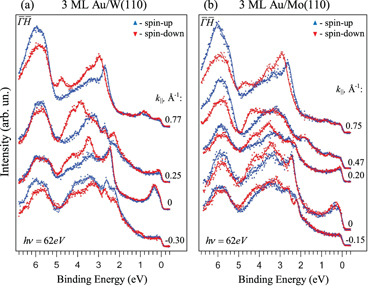
Figure 5. Angle- and spin-resolved EDCs for 3 ML of Au on W(110) (a) and on Mo(110) (b) for k∥ along  in a wide energy region including the Au 5d band. The value of k∥ refers to electrons at the Fermi level.
Download figure:
Standard image High-resolution imageIt follows from the crystal symmetry that the spin polarization of the initial states is antisymmetric in k∥. However, the photoemission setup destroys the symmetry, so the spin polarization of the photocurrent does not follow that of the initial states. In [21, 23], this has been shown to lead to a deviation of the k∥ distribution of the photocurrent from the antisymmetric picture and to a polarization of the normal emission spectrum. Although the polarization of the photocurrent at k∥ = 0 depends on the photoemission setup, the ultimate origin of this effect lies in the spin structure of the ground state: it is a consequence of the initial state wave function not being a spin eigenfunction, but a two-component spinor where both components are non-zero. Here the asymmetric photoemission setup reveals the non-trivial spin structure of the initial states, which originates from the spin–orbit coupling. Usually, the Rashba effect is formulated in terms of spin densities (see figures 7 and 9) and in this sense it does not occur at k∥ = 0. Angle-resolved photoemission goes beyond this simple formulation; the close similarity of the spin-resolved EDCs at  in figure 5 serves as another indication of a weak interaction of Au d QWS with the substrate.
5. Discussion
In order to understand the nature of the experimentally observed spin-polarized structures, let us first consider a more transparent case of QWSs in a nearly free-electron metal. Based on calculations of Krasovskii and Chulkov [22], we present in figure 6 the dispersion E(k∥) of QWSs in a 19-layer symmetric Al(111) slab.
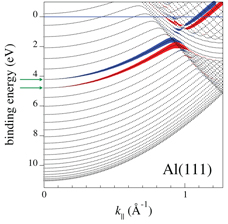
Figure 6. Entanglement of spin polarization and quantum well splitting for a 19-layer Al(111) slab. Black dots show the dispersion of the quantum well energy levels along  , each level containing two Kramers-degenerate states. The size of the blue (spin ↑) and red (spin ↓) full circles is proportional to the net-spin spectral density Stot(E,k∥) obtained with γ = 0, see section 3. The two energy levels indicated by the horizontal arrows at the energy axis contain the four QWSs that evolve with increasing the film thickness into the spin-degenerate surface states—two Rashba-split states at each surface. In the finite slab, the two levels are (oppositely) polarized much stronger than the levels that evolve into bulk continuum. See also [22].
Download figure:
Standard image High-resolution imageAlthough the spin polarization in Al is too small to be detected experimentally, the case of Al(111) is very instructive owing to its simple and well-known electronic structure. It exemplifies the simplest case of Rashba polarization (as opposed to Rashba splitting). In figure 6, all states are doubly degenerate; the energy splitting here is the quantum size effect—the splitting occurs between Kramers-degenerate pairs of states. (Each data point—red or blue circle—is a sum over the degenerate pair, see equation (1) and the explanation in section 3.) The spin polarization is seen to be unevenly distributed over the spectrum; it is by far the strongest for the two quantum well levels that would evolve into the surface states by increasing the film thickness (the two levels are indicated by arrows in figure 6). This means that the quantum well splitting (in this case of the order of 0.5 eV) is accompanied by (entangled with) the spin polarization. This demonstrates that the spin structure of QWSs cannot be understood as an energy splitting solely due to the spin–orbit interaction and that the quantization effect plays a major role here.
In the limit of large thicknesses, the two quantum well levels would evolve into four surface states, two states on each of the two surfaces. (Thereby the spin–orbit coupling disentangles from the quantum well effect.) The pair of states on one surface would be the Rashba split states, which would be 100% polarized, but in aluminum their energy splitting is below any conceivable experimental energy resolution. Thus, the difference between the Rashba effect for surface states and for QWSs of a symmetric film can be understood by considering a gedanken experiment with a rough energy resolution and an unlimited spin sensitivity. For aluminum, the effect for surface states would not be observed, whereas for the quantum well system, the effect can be observed even with an energy resolution of 0.5 eV.
5.1. Quantum well states of Au 5d band
Naturally, the spin structure of QWSs becomes much more complicated in the Au overlayer, where the spin–orbit splitting is comparable with the finite-thickness effect. The calculated electronic structure of Au/W(110) and Au/Mo(110) is presented in figure 7 in terms of k∥-projected DOS functions. The band structure of the substrate is reflected in the total DOS maps (figures 7(a) and (d)) in the lower energy location of the W sp band relative to its Mo counterpart. The partial Au overlayer projected DOS functions (figures 7(b) and (e)) are, on the contrary, very similar. Below 2 eV, they show two high-intensity (red-yellow) bands of Au 5d QWSs separated by a low-intensity region around 4.5 eV. The two wide bands are clearly seen in the measured spectra of figure 5, with the gross features being shifted to lower energies by about 0.5 eV, as expected for an LDA calculation (see section 3). In the d band region, one cannot resolve spin-related pairs of dispersion lines; the net-spin density has a complicated distributed character (figures 7(c) and (f)). Nevertheless, the spin structure of the d states in the two systems is almost identical. This is a consequence of a very weak interaction of the localized d states with the substrate. To demonstrate this, we present in figure 8 the local spectral functions for the two surfaces for k∥ = 0.56 Å−1. The d states between 2 and 7 eV are seen to be essentially the same, even though in the case of W(110), the lower part of the Au 5d band energetically overlaps with the sp band of the substrate and in Mo(110) it does not. The k∥ projected polarization pictures are also nearly the same, and the first thing to notice is that the net spin density is strongly position-dependent. Clearly, the spectral density features cannot be understood as spin–orbit-split pairs, which is the consequence of the entanglement of the spin polarization and quantum well splitting mentioned in the beginning of the section.
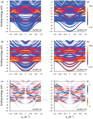
Figure 7. Total and partial k∥-resolved DOS functions for Au/W(110) (left panels) and Au/Mo(110) (right panels). Graphs (a) and (d) show total DOS N(E,k∥), (b) and (e) partial DOS NAu(E,k∥) and (c) and (f) partial net-spin DOS SAu(E,k∥). The functions are obtained with the broadening of γ = 0.25 eV. For notation, see section 3.
Download figure:
Standard image High-resolution image
Figure 8. Spatially resolved spectral functions for 23-layer slabs of Au/W(110) (left panels) and Au/Mo(110) (right panels): total k∥-resolved DOS ρ(z,E) and spin DOS σ(z,E) for k∥ = 0.56 Å−1 obtained with γ = 0.25 eV.
Download figure:
Standard image High-resolution image5.2. Quantum well states of sp band
The sp QWSs are seen in the calculated partial DOS maps in figures 7(b) and (e) as rapidly dispersing features above 2 eV. A magnified picture of the sp QWSs is presented by figure 9. The delocalized states are seen to be much more strongly polarized in Au/W(110) than in Au/Mo(110), cf figures 9(b) and (d), where the differences are indicated by arrows. To understand the origin of the experimentally observed spin-polarized structures coming from the sp QWSs, we show in figure 10 depth-resolved k∥-projected DOS functions ρk∥(z,E) and σk∥(z,E) calculated for the 23-layer slabs of Au/W(110) and Au/Mo(110). First, we consider the two structures denoted α, located at about 1 eV binding energy for both substrates, see figures 9(b) and (d). The total DOS maps ρk∥(z,E) show that their spatial structure is also very similar for W and Mo: they are localized in the region comprising the last atomic layer of the substrate and the Au overlayer. Although they lie in the local k∥-projected gap of the bulk band structure, they strongly interact with the substrate, which energetically manifests itself in their splitting being twice as large for W than for Mo. Clearly, this is a result of the stronger spin–orbit interaction at the tungsten sites. Note, however, that not only the splitting but also the spin polarization σk∥(z,E) is strongly enhanced. This means that the relativistic effect does not follow the scenario of the simple RB model, in which the states are spin eigenfunctions, i.e. they are fully polarized, irrespective of the magnitude of the splitting. Thus, we interpret the structures between 1.2 and 1.5 eV in the Au/W(110) spectra for k∥ = −0.56 and +0.58 Å−1 as coming from the α-QWSs. Figures 9(b) and (d) clearly show that above the binding energy of ∼0.8 eV, the energy sequence of the spin components of α-branch is opposite in Au/W(110) and Au/Mo(110), an observation already made in section 4 regarding the experimental spectra in figure 4. The above analysis ascribes the different behavior of the photocurrent to the spin structure of the initial states and relates it to the influence of the substrate.

Figure 9. Partial k∥-resolved DOS functions for Au/W(110) (left panels) and Au/Mo(110) (right panels). Graphs (a) and (c) show total DOS NAu(E,k∥); the two arrows indicate the different structure of the spectral density lines in the two systems. Graphs (b) and (d) show partial net-spin DOS SAu(E,k∥); the two sets of six arrows in (b) and (d) are identical: they point to the differences between the net-spin spectral functions in the two systems. Labels α and β indicate the two dispersion branches analyzed in figure 10. The functions are obtained with the broadening of γ = 0.05 eV. For notation, see section 3.
Download figure:
Standard image High-resolution image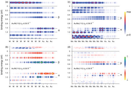
Figure 10. Spatially resolved spectral functions for sp QWSs on Au/W(110) (a), (b) and Au/Mo(110) (c), (d): total k∥-resolved DOS ρ(z,E) and spin DOS σ(z,E) for k∥ = 0.58 Å−1 obtained with the broadening of γ = 0.05 eV. Labels α and β correspond to the notation in figure 9.
Download figure:
Standard image High-resolution image
The QWSs β located at 0.5 eV also have a resonant character but, according to figures 10(a) and (c), they are much stronger delocalized than α-QWSs. Consequently, the effect of the spin–orbit interaction in the substrate is much stronger: not only the polarization of the lower-lying state dramatically increases in Au/W(110) but also its opposite-spin counterpart is pushed upwards and merges with the bulk continuum, see figures 10(b). (There is the double β-branch for Au/Mo(110) and the single one for Au/W(110). This is a consequence of the different structure of the spectral density lines in the two systems, as indicated by the arrows in figure 9.) The structure β is not visible in the spin-resolved spectra, apparently because it is buried under the Au overlayer, but in the second-derivative map of figure 3, one can discern a line corresponding to this structure.
6. Conclusion
The spin- and angle-resolved photoemission study of the 3 ML Au overlayers on W(110) and Mo(110) reveals the spin–orbit-induced spin structure of the QWSs of Au 5d and sp character. Both the energy and the spin structure of the Au 5d QWSs is found to be virtually the same for Au/W(110) and Au/Mo(110), whereas for the sp QWSs, an enhanced splitting is observed on the W(110) substrate. These results are explained by a theoretical analysis based on a finite-thickness-slab calculation for a realistic model of the overlayer system. The theory confirms a negligible interaction of the localized Au 5d QWSs with the substrate and an appreciable penetration of the delocalized sp QWSs into the substrate. For the sp QWSs, the spin–orbit interaction on the tungsten atom increases both the energy splitting and the degree of polarization. This reveals the deviation of the spin structure of QWSs from the simple picture of the RB splitting of surface states, in which the degree of polarization does not depend on the magnitude of the energy splitting. This behavior is a manifestation of the quite general phenomenon of the entanglement of quantum well splitting and spin–orbit-induced spin structure.
Acknowledgments
This work was supported by a grant from the Saint–Petersburg State University for scientific investigations and the Russian Foundation for Basic Research (RFBR) project 11-02-00642-a and performed in the framework of a collaboration between the Deutsche Forschungsgemeinschaft and the Russian Foundation for Basic Research (numbers 13-02-91327, 13-02-91336 and RA 1041/3-1). The authors acknowledge support from the Russian–German laboratory at BESSY II (Helmholtz–Zentrum Berlin) and AAR, EVZ and IIK acknowledge support from the German-Russian Interdisciplinary Science Center (G-RISC) funded by the German Federal Foreign Office via the German Academic Exchange Service (DAAD). The authors acknowledge partial support from the Spanish Ministerio de Ciencia e Innovación (grant number FIS2010-19609-C02-02).