Abstract
We provide an overview of the development of a merged system of low-temperature ultrahigh-vacuum scanning tunneling microscope (STM) with photon collection and detection units for optical imaging at the nanoscale. Focusing on our own work over the past ten years, the paper starts from a brief introduction of the STM induced luminescence (STML) technique and the challenge for nanoscale optical imaging, and then describes the design and instrumentation on the photon collection and detection system. The powerful potentials of the technique are illustrated using several selected examples from STML to tip enhanced Raman scattering that are mainly related to photon mapping. Such photon maps could reveal not only the local electromagnetic properties and the nature of optical transitions in the junction, but also exhibit spatial imaging resolution down to sub-molecular and sub-nanometer scale. The paper is concluded with a brief overlook on the future development of the STML technique.
Export citation and abstract BibTeX RIS
1. Introduction
Nanoscale imaging by photons and electrons is indispensible for nano-characterization, particularly important for understanding and control of nanomaterials. Various fluorescence techniques including stimulated emission depletion microscopy,1) stochastic optical reconstruction microscopy,2) and photoactivated localization microscopy3) have been elegantly developed by statistically controlling the optical states of fluorescence-labelled molecules, which can go beyond diffraction limit and provide far-field spatial resolution down to ∼10 nm. An alternative approach to improve nanoscale imaging is to make use of plasmonic effects via a metallic tip4–6) or a metallic thin-film superlens,7) but the spatial resolution achieved by the near-field optical techniques8) is still difficult to go below 10 nm.
By contrast, the tunneling electrons in a scanning tunneling microscope (STM) can be used to not only image and manipulate surface nanostructures with atomic resolution, but also excite light emission from the STM junction through inelastic tunneling. This technique is called STM induced luminescence (STML)9–12) and can do nano-imaging beyond classical optics and plasmonic effects thanks to the highly localized nature of tunneling electron excitation. Photon maps with unmatchable spatial resolution down to sub-nanometer scale have been demonstrated.13–20) Moreover, in addition to the atomically resolved topographic and conductance information provided by the electron tunneling signals, the photon signals obtained via the STML technique are associated with inelastic tunneling channels and can thus provide additional information on the decay of various local electromagnetic excitations that are usually unavailable by STM imaging alone. Consequently, the STML has emerged as an important real-space technique to investigate optical phenomena at the nanoscale, particularly powerful for gaining insight into the optoelectronic behavior of single molecules in a nanoscopic environment. Furthermore, when the technique is further combined with Raman spectroscopy, nanoscale spectral mapping can offer great promise to the chemical identification of species on the surface down to the single-molecule scale.20)
STM-based photon mapping, with either photon intensity or spectral information simultaneously recorded for each pixel of an STM image, has been repeatedly reported to achieve optical contrast on the molecular scale for molecule-covered surfaces,13,14,17–24) but high-quality photon maps with sub-molecular resolution are relatively rare, amounting to mainly HBDC on Cu14) and porphyrin molecules on oxidized NiAl.16–20) One of the main reasons for such limited reports is due to the very low quantum efficiency of photons produced by tunneling electrons, usually in the range of 10−5 to 10−3 photons per electron on both metal surfaces25–28) and molecular systems.14,23,24,29–31) Such low efficiency imposes a great experimental challenge to acquire photon signals with good signal-to-noise ratios. That is partly why early photon-map data for molecular systems were usually acquired with large currents (nA typically,13,21–24) with only a couple of recent examples14,16–19) going down to sub-nA) and long integration time (several ten milliseconds per pixel or more).
The STM induced luminescence is known very sensitive to the tip status,14,32) STML experiments carried out at high currents may modify both molecules on surfaces and tip conditions easily, while long integration time would require a thermally very stable system to avoid the thermal drift problem. The latter usually not only requires expensive cryogenic conditions such as in liquid helium,14,17) but may be also a bit demanding when optical access to the junction area is required. Therefore, it is highly desirable to drive down both tunneling currents and integration time as small as possible for photon mapping measurements so that both molecules and tips can be free of damage, allowing to acquire clean and reliable mapping data under the same tip condition and within a relatively short time. Similar requirements also apply to the non-invasive spectral measurements, particularly for single-molecule electroluminescence studies where the molecule is decoupled by a dielectric spacer from the substrate and the sample conductivity is usually very low.
In this paper, we present an overview of our instrumental development that combines a custom-designed low-temperature ultrahigh-vacuum (UHV) STM with photon collection and detection systems for optical measurements of luminescence spectra and photon maps. We do not intend to provide a comprehensive review in the field, rather focusing mainly on our own work over the past ten years. We shall also stress more on the technical side, without detailed discussion on the underlying physics involved in the STML process such as the critical role of resonant nanocavity plasmons in enhancing and shaping molecular electroluminescence.12,33) It is our hope that what we present here can serve as a research tutorial, providing basic technical information to the newcomers of the STML field so that they can know what kind of factors to consider when designing STML setups, what kind of data to measure when doing experiments, and what kind of research fields to apply for this technique. The paper is organized as follows. After a brief introduction of STML, we provide in Sect. 2 a detailed discussion on the design and instrumentation of the photon collection setup adopted in our lab. Section 3 is devoted to photon detection. Following a brief introduction on the various modes of STML measurements, we use several selected examples to demonstrate the powerful potentials of this technique for the spectral measurement, intensity-based photon mapping, and "color" spectroscopic imaging. The paper is concluded with a brief perspective on the future development of the STML technique.
2. Photon collection in STML
2.1. Modes of photon collection
Since the photon signals emitted from the nanoscale STM junction are very weak, the guideline for the instrumental design of photon collection units in a UHV-STM is to achieve a collection angle as large as possible and also to enable convenient operation on optical alignment, under the condition not to degrade the STM performance itself. According to our experience, efficient photon collection is one of the most important keys to a successful STML experiment. Therefore, in this section, we shall give a further broadened description of the optical setup given in Ref. 19.
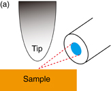
There are three kinds of photon collection methods documented in the literature, namely, fiber or fiber bundles [Fig. 1(a)],34–39) ellipsoidal or parabolic mirrors [Fig. 1(b)],18,40–43) and lens setup [Fig. 1(c)].44–48) In the fiber system, an optical fiber is placed close to the tip–sample junction in order to achieve a large collection angle. However, in addition to the difficulty in optical alignment, great care should also be taken to avoid the collision of the fiber with the sample and tip during transfer and operation in UHV. An effective hemisphere solid angle coverage of ∼0.053 sr has been reported for the light collection in UHV using the fiber system.39) The relatively small collection efficiency was attributed to inaccuracies in assembling the fibers. Note that the use of a conducting fiber tip for light collection has also been reported.49,50) Although the theoretical collection efficiency could be high for the near-field fiber tip, the control on both the quality of tip apex and the photon coupling to subsequent connecting fibers (including both inner and outer UHV) remains quite challenging. On the other hand, the parabolic or ellipsoidal mirror has been reported to offer a large hemisphere solid angle coverage up to ∼3 sr,40) which could also avoid both spherical and chromatic aberration. Therefore, theoretically, the ellipsoidal mirror could be an ideal system for photon collection. However, the fabrication of an ellipsoidal mirror inside UHV and subsequent optical alignment are very challenging. By contrast, the lens system has proven to offer a suitable hemisphere coverage of solid angles, usually sufficient for collecting strong-enough photon signals to make spectral measurements with good signal-to-noise ratios and within reasonable integration time. Most importantly, the lens system has the technical advantage of simple and easy optical alignment, and is thus the configuration we selected for our optical setup (Fig. 2). In the following, we shall describe several factors that should be considered for the optimization of photon collection units, including the design of the collimating lens and its axial orientation, the in-situ lens adjustment system for optical alignment, and the light coupling outside UHV.
Download figure:
Standard image High-resolution image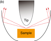
Download figure:
Standard image High-resolution image
Fig. 1. Three different configurations for collecting the emitted photons from the tunnel junction: (a) optical fiber, (b) mirror, and (c) lens.
Download figure:
Standard image High-resolution image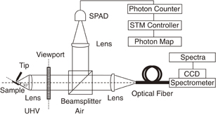
Fig. 2. Schematic setup of a UHV-STM system equipped with an inner-UHV lens for photon collection. Collected photons are guided into either a photon detector such as SPAD for intensity and photon map measurements or a CCD spectrometer for spectral measurements.19)
Download figure:
Standard image High-resolution image2.2. Optical optimization
Taking into account the space available around the tunnel junction and also for locating the lens stage inside a low-temperature UHV-STM chamber, we have designed an aspherical collimating lens that could produce a large hemisphere solid-angle coverage up to ∼0.8 sr.19) Since the plasmonic emission from the tunnel junction is known to maximize along the direction about 60° off the surface normal,51) the optical axis of the collimating lens is designed to orient along this direction, as illustrated in Fig. 2. Considering the practical situation of etched tip shapes, a cone angle of ∼60° along the optical axis appear approaching the limit of the open space available for a given direction.
In our optical setup, a plano-convex aspherical lens with a diameter of D1 = 25 mm (te = 2 mm and tc = 10 mm) and a front focal length of f1 = 19.5 mm is adopted for the collimating lens inside UHV via the optimization using the Zemax software.52) Since those photons reaching the lens edge will be blocked by the lens holder, the effective aperture of the lens inside UHV is actually smaller, ∼22.2 mm. As shown in Figs. 2 and 3(a), this collimating lens is designed to guide collected photons into a nearly parallel beam, which passes the quartz viewport and is then re-focused by another plano-convex aspherical lens outside UHV (D2 = 30 mm, f2 = 70 mm) into an optical fiber (NA = 0.2 according to design) for spectral measurements or directly onto a single photon avalanched photodiode (SPAD) for photon intensity measurements.

Fig. 3. (a) Three-dimensional layout of our double-lens setup. (b) Focus spot diagram on the image plane. (c) Fraction of enclosed energy as a function of radius from the spot center. (d, e) Coupling efficiency for different central wavelength at 650 and 560 nm, respectively. (f) Configurations of the optical fiber bundle, (left) the receiving end; (right) the output end coupled to the spectrometer. Reprinted from Ref. 19 with permission from American Institute of Physics.
Download figure:
Standard image High-resolution imageThe selection of aspherical lenses rather than spherical is based on the consideration of reducing the spherical aberration of off-axis ray and has proven crucial for efficient photon collection. The aspherical lens can increase the effective aperture size and also reduce the spot size at the image plane. The wavelength of 650 nm is used in our optical optimization since the major emission band of porphyrin molecules that we usually use in our experiments is around this wavelength. The designed aspherical lens inside UHV can yield an effective hemisphere solid-angle coverage of ∼13% (namely, Ω = 0.82 sr or NA = 0.5) after taking into account the effective aperture size of ∼22.2 mm. To our knowledge, such an effective collection efficiency is larger than what has been reported to date for a single lens system. As shown in Fig. 3(b), the optimized spot size at the image plane is quite small, with a geometry radius of 56 µm, which means all photons emitted at 650 nm can be collected once the sensor size (or the fiber diameter) is larger than 112 µm [Fig. 3(c)]. By contrast, if the optical simulation is performed with a spherical-shape lens configuration, a small focus spot (e.g., 200 µm) would make the aperture size of the collimating lens very small (e.g., 6–7 mm). On the other hand, a large aperture size such as 22.2 mm would make the focus spot very large (even using a collector with a diameter of 1.4 mm, the fraction of collected photons is still only 50%). Evidently, the aspherical lens is advantageous over the spherical lens in terms of the photon collection efficiency. Note that the use of the aspherical lens design becomes extremely critical for efficient photon collection when photons emit over a wide cone angle (i.e., requiring large aperture size) and/or the distance between the inner and outer UHV lenses is relatively long.
Although a single convex aspherical lens is good at correcting the spherical aberration, it is not effective in calibrating chromatic aberrations. In traditional optics, a double-lens or compound-lens system is usually employed to correct the spherical and chromatic aberrations so that the spot size at the image plane can be reduced. However in our UHV system, such design cannot be readily implemented due to the limitations on the available space, low temperature and ultrahigh vacuum requirements. In addition, the use of additional lens will also lead to photon loss and difficulty in optical alignment, not to mention that it is highly challenging to make a combination-lens system inside UHV capable of good focusing over a wide spectral range in the visible. Therefore, the simple double-lens system is usually adopted for collimating and condensing photons in the lens setup inside UHV. But to compensate the photon loss caused by the chromatic aberration, two approaches are usually employed, one is to use a fiber or sensor that has a relatively large area for photon collection or detection, the other is to have a simple but precise lens adjustment system so that the optic setup can be aligned to work at different central wavelengths as desired.
Figure 3(d) plots the wavelength-dependent coupling efficiency at 650 nm between the double-lens system in Fig. 3(a) and photon collector located at the focal point on the image plane, respectively for a collector diameter of 170, 400, and 1200 µm; whereas in Fig. 3(e), a similar plot is presented for a central wavelength at 560 nm (which is often the plasmonic emission maximum for Ag tips on the Ag surface). As illustrated in Figs. 3(d) and 3(e), the chromatic aberration is less serious when the optic setup is aligned to work at the designed wavelength of 650 nm for optical optimization. The three kinds of dimension information mentioned above correspond to the diameter of the SPAD sensor, the core diameter of a single multi-mode fiber, and the diameter of a fiber bundle in our practical setup, respectively. Because of the chromatic aberration and the small size of the SPAD sensor (∼170 µm), collected photons could be lost when focusing onto the sensor if the emission band is very broad. But for spectral measurements via the fiber bundle shown in Fig. 3(f), the chromatic aberration does not appear to be a problem because the full emission band can usually be measured using the central single fiber with a core diameter of 400 µm, and even if the emission band is very broad, the photons can still be collected by the additional peripheral six fibers in the bundle. The left part of Fig. 3(f) shows the receiving end of the optical fiber bundle used in our experiments, composed of one fiber at the center and other six fibers arranged in a concentric hexagonal pattern. On the right of Fig. 3(f), the seven individual fibers are arranged into a line shape that can be conveniently coupled to the slit of a monochromator. The image was measured using the spectroscopic imaging mode of a charge-coupled-device (CCD) spectrometer for the STM-induced plasmonic emission on Ag peaked at ∼560 nm. The fiber at the bottom marked as "1" corresponds to the central fiber in the left of Fig. 3(f). The predominant brightness at the CCD detection position corresponding to fiber #1 indicates that most photons can be well condensed into the central single fiber, providing a clear demonstration of an efficient operation of our designed optical system.
The use of aspherical lenses requires good focusing for optimal operation, otherwise the photon signals will lose significantly. Therefore, the in-situ lens adjustment along three translational directions inside UHV is critical for a convenient and precise optical alignment. In our setup, all lenses are mounted on a stage with three translational degrees of freedom. For the lens inside UHV, its motion can be controlled by piezoelectric motors operated in the slip-stick mode with a precision of about 1 µm. With the assistance of a video camera outside UHV, the lens adjustment for optical alignment can be monitored easily through the image formed at the focus point of the image plane. It is worthy to mention that, in order to reduce the photon loss and widen the range of spectral measurements, the materials of all lenses and optical viewports are made of fused silica.
Depending on the measurement modes of interest, the light coupling outside UHV is also important for optimal operation. For spectral measurements, as discussed above, it is very convenient to re-focus the collected photons into a fiber or fiber bundle with reasonable core diameters, which can then be coupled to a spectrometer to obtain the spectral information with little suffering from the chromatic aberration problem. However, for absolute light intensity measurements (including photon mapping) by the SPAD and characterization of photon emission properties such as polarization and coherency, it is highly desirable to adopt a free-space coupling mode with the capability to add in filters or polarizers. Of course, the insertion of a beamsplitter into the optical path can allow simultaneous measurements in both modes, as shown in Fig. 2. Moreover, the fiber-free coupling of light directly onto the ultrasensitive SPAD also has the advantage to avoid photon loss due to the fiber coupling. The optimal combination of good optical alignment and coupling with highly efficient optical detection that reaches the single-photon sensitivity (plus a strongly emitting STM tip) will allow one to perform photon mapping experiments at low currents and short exposure time. It is worth mentioning that the use of such mild experimental conditions is particularly useful for carrying out clean and non-invasive STML measurements on poorly conducting samples.
3. Photon detection
3.1. Modes of measurements
Before proceeding to the description of various modes of STML measurements, let's first see what kind of photon detectors are required in order to detect the photon signals efficiently. The intensity of photons emitted from the STM junction in the STML experiments is usually very weak because on one hand, these photons are generated through an inelastic tunneling process and the quantum efficiency of photons produced by tunneling electrons is usually low (∼10−5 to 10−3 photons/electron); and on the other hand, these photons originates from a very small tunnel junction down to nanoscale or even from a single molecule. Therefore, photon detectors with single-photon sensitivity and low dark noise are desirable for STML experiments. The most common detectors used are avalanche photodiodes (APD), photomultiplier tubes (PMT), and CCD. The selection of photon detectors depends on the modes of measurements, usually based on a comprehensive consideration over the quantum efficiency, the range of wavelength of interest, the time response, the dark current noise, and the sensor size.10)
There are a number of modes reported in the existing STML measurements that are used to explore different aspects of the local electromagnetic properties and electron-to-photon conversion process at the nanoscale junction. These include luminescence spectra, isochromatic spectra, intensity-based photon mapping, spectroscopic imaging (the so-called "color" photon mapping), light polarization analysis, and time-correlated emission statistics measurements. The wavelength-resolved luminescence spectra could reveal direct information on the nature of optical transitions involved; The isochromatic spectra, measured as a function of tunneling bias at constant tunneling currents, could reflect the influence of the excitation energy on the intensity of a specific emission; The intensity-based photon mapping and "color" spectroscopic imaging could show site-specific light emission properties that not only offer insights into the influence of local geometry, local electronic states and local environment on the observed dipolar emission, but also enable a panoramic view of chemical identification and mapping of surface species at the nanoscale through fluorescence or Raman spectral fingerprints; The light polarization analysis could provide information on the emitting dipole orientation in a tunneling junction; The time correlation measurement could reveal fluorescence decay dynamics and photon emission statistics such as bunching or antibunching. In this paper, we mainly focus on the three most common modes used so far, namely, the measurements of luminescence spectra, intensity-based photon mapping, and "color" spectroscopic imaging.
To make the story complete, we would also like to say a few words about the tip issue in STM-based light emission experiments since the quality of optical data measured depends critically on the quality of the tip used. The STM tip material is known to have a great influence on the light emission spectra because the resonance frequency and the field strength of the nanocavity plasmon are closely related to the dielectric properties of both sample and tip. This has been illustrated by STML experiments using different combinations of tip (W, Ag, Au) and sample (Ag, Au) materials.26,55) The strongest light emission is observed when using silver (Ag) metal tips, which can provide STML intensities about one order of magnitude stronger than that by tungsten (W) tips.55) The high photon yield obtained with a Ag tip is due to the small imaginary component of its dielectric constant and resultant low optical damping loss.53) Therefore, Ag tips are considered to be the best tip material for generating strong plasmonic fields, which is known to play a very important role in the generation of strong molecular luminescence and Raman scattering signals.12,31,54) For how to make a high-quality Ag tip, please see Ref. 28 and references cited therein.
3.2. Selected examples of STM induced luminescence
Before presenting selected STML examples, we would like to make a note on the vacuum level and temperature used in our experiments and why UHV–LT conditions are desirable for single-molecule studies. All the experimental data presented in this paper were measured on a custom UHV–LT-STM under a base pressure of ∼1 × 10⁻¹⁰ Torr at ∼80 K unless otherwise specified. The UHV–LT condition is advantageous for single-molecule studies. Under UHV conditions, both the tip and sample surface can be cleaned up easily and maintained clean, minimizing otherwise serious contamination in ambient conditions and thus enhancing the stability of the tip–sample junction. In addition, clean molecular samples can be prepared via vacuum deposition onto surfaces with a controlled coverage. The latter is particularly important since the presence of isolated single molecules on surfaces is desirable for well-defined single-molecule measurements. In this regard, a substrate cooled to low temperature is also very helpful for isolated single molecules to immobilize on the surface, thus suppressing the diffusion and desorption problem. Moreover, the thermal drift problem can also be suppressed at low temperature, and the UHV condition can also significantly decrease photodegradation of adsorbed molecules, thus allowing molecules to be measured with longer time and repeatedly for light excited fluorescence and Raman experiments.
3.2.1. Luminescence spectra
The wavelength-resolved luminescence spectra are probably the most common and most important data to measure in STML experiments since the spectral profile and peak positions can directly reveal the local electromagnetic properties and the nature of optical transitions involved. Therefore, before we proceed to the description of photon mapping with photon signals recorded simultaneously to each pixel of an STM image during scanning, we would like to show briefly how single-point spectral data can be used to understand the electroluminescence phenomena observed.
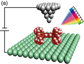
Photon emissions from clean metal surfaces are attributed to the radiative decay of the local surface plasmon through inelastic tunneling excitations by a metallic tip.26,55) However, when an organic molecule is adsorbed directly on a metal surface, the light emission from the ad-molecule is still plasmonic in nature14,21,56–61) (unless the emitting molecule is specially designed with built-in spacers62)). This is because the radiationless energy transfer from the molecular excited state to the metal substrate is much faster than the radiative decay process, leading to the quenching of molecular fluorescence. Such justification can be easily made by comparing the emission spectrum on the ad-molecule with that on the bare metal surface. As shown in Fig. 4, although the STML spectra acquired above the Zn-centered tetraphenylporphyrin (ZnTPP) ad-molecules are strongly suppressed, their spectral profiles are essentially the same as those measured from the bare metal surface, which clearly indicates a plasmonic nature for the emitted photons and the quenching of molecular fluorescence.63)
Download figure:
Standard image High-resolution image
Download figure:
Standard image High-resolution image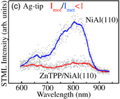
Fig. 4. (a) Schematic diagram of STM induced luminescence from a molecular junction. (b) Photon emission spectra acquired from bare Au(111) and ZnTPP islands (2.5 V, 0.5 nA, 165 s). (c) Photon emission spectra acquired from bare NiAl(110) and ZnTPP molecules (2.5 V, 0.3 nA, 300 s).63) The STML data were measured at ∼5 K.
Download figure:
Standard image High-resolution imageIn order to generate molecule-specific emissions, the emitting molecule has to be sufficiently decoupled from the underlying metal substrate to suppress fluorescence quenching. Such electronic decoupling can be usually realized by either inserting a dielectric spacer layer such as oxides29,64) or using molecular multilayers,30,31,54,65–67) or a combination of both molecular and dielectric layers.48,68,69) STML spectra could provide the most straightforward and authoritative evidence for the successful generation of intrinsic molecular fluorescence if in combination with standard optical data of the molecules. As illustrated on the right of Fig. 5(c), the STML spectra on a multilayer molecular sample of tetraphenylporphyrin (TPP) are characteristic of several sharp emission peaks, which is distinctly different from the corresponding spectra on the pristine metal surface [left spectra of Fig. 5(c)].31) By correlating with the known optical data and electronic structures of porphyrin molecules, these emission peaks can be readily assigned to the π*–π transitions associated with the radiative decay of molecular excited states back to the ground state.70) Furthermore, judging from the evolution of spectral profiles along with the nanocavity plasmonic modes, we can conclude that the nanocavity plasmon plays an important role in the resonant enhancement of selected emission channels, shaping the emission profile dramatically and even generating relaxationless molecular hot-electroluminescence that goes beyond Kasha's rule and is usually "forbidden" in conventional molecular spectra.33)
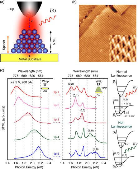
Fig. 5. (a) Schematic junction geometry with multi-monolayer molecular stacking and localized electrical excitation from a nanotip. (b) STM images showing highly ordered five-monolayer TPP molecules on Au(111) (55 × 55 nm2, +2.5 V, 2 pA). The inset is a high resolution image (6 × 6 nm2, +2.5 V, 2 pA). (c) Left: STML spectra from a pristine gold surface, showing different nanocavity plasmon resonance modes that are tuned to match particular radiative transition of the TPP molecules. Middle: Corresponding STML spectra taken above the molecular sample in (b) using the particularly defined W tip status on the left. Right: Schematics for the vibronic transitions for normal luminescence and hot luminescence.31)
Download figure:
Standard image High-resolution image3.2.2. Intensity-based photon mapping
Intensity-based photon maps can provide a panoramic view of optical contrast of various surface nanostructures, which could also greatly facilitate the investigation of specific sites of interest on the surface. Such intensity-based photon maps are recorded simultaneously with topographic image by storing at each pixel the photon intensity detected by either a PMT or an APD, usually in the all-pass mode. If emitted photons are filtered by narrow bandpass filters for certain specific spectral peaks, such photon map may also provide the spatial distribution of chemical-specific nanostructures on the surface. In addition, the site-specific optical contrast can also offer insights into the influence of local geometry, local electronic states, and local environment on the light emission properties.
Figure 6 shows one example of such intensity-based photon map applied to the STML study of H2TBPP porphyrin molecules on Ag(111). It is worth mentioning that the optical optimization addressed above, together with the assistance of a strongly emitting tip, enables us to achieve high photon count rates using relatively small currents and relatively short exposure time per pixel. The photon count rate detected by the SPAD could reach up to an average of ∼39.4 × 10³ cps on the bare Ag surface at a current of 10 pA. Since the average calibration factor for the photon collection and detection efficiency of our optical setup is ∼3.9%, the detected count rate corresponds to a very high quantum efficiency of ∼1.6 × 10⁻² photons per electron.19) In this sense, our technical advancements also provide experimental data that would demand more sophisticated theoretical understanding on the nanocavity plasmonic emissions in STM.

Download figure:
Standard image High-resolution image
Fig. 6. (a) and (b) Simultaneously acquired STM image and photon map of sub-monolayered H2TBPP molecules on Ag(111) over a relatively large area (+2.5 V, 20 pA, 100 × 100 nm2, 512 × 512 pixel, 2.0 ms/pixel).
Download figure:
Standard image High-resolution imageThe mild imaging condition at low currents and short exposure time allows us to do photon mapping with suitable resolution over a relatively large area (e.g., 100 × 100 nm2 as demonstrated here in Fig. 6). The panoramic view over a large area facilitates the simultaneous observation and comparison of optical contrasts of different structures on the surface, such as the molecular chains along the step edges and isolated molecules or clusters or molecular islands on the terrace. Furthermore, the spatial resolution of the photon map in Fig. 6(b) is comparable to the molecular resolution of the STM image in Fig. 6(a), also revealing the stripe-like pattern for the molecular packing. Since each H2TBPP molecule is directly adsorbed on the Ag surface, the photons emitted are still plasmonic in nature and the molecular fluorescence is quenched.19) However, as illustrated in the photon map, the emission on the bare Ag surface appears brighter than that on the molecular island, which suggests that the molecule may act mainly as a geometrical spacer, reducing the local field strength with the increased gap distance when a molecule is inserted into the tunnel junction.71) A more precise quantitative comparison can be realized through higher-resolution photon mapping over a smaller area, as demonstrated below.
Figure 7(a) shows a higher-resolution STM topograph with simultaneously acquired photon map in Fig. 7(b), which reveals two pronounced features. The first one is the overall "inverse" contrast between the height in the topographic image and the intensity in the photon map. The photon intensity above the molecular island is lower than that on the bare Ag surface. Note that the photon emission at the island edges (or edges of isolated molecules or molecular chains) becomes even stronger than that on the bare Ag surface. Such edge-enhanced emission is believed to originate from the change in the local electronic states and will be addressed in detail elsewhere. The second feature in Fig. 7(b) is the change of stripe orientations in terms of dark or bright feature inside a stripe (by about 90°) from the topographic image to the photon map. A careful investigation suggests that on the molecular island, the photon emission from the inter-molecular sites is slightly stronger than that from the intra-molecular sites, which might be responsible for the orientational change of stripe features. These observations out of high-resolution photon maps may also suggest the involvement of the same underlying physics for the slightly stronger emission at the inter-molecular sites as in the edged-enhanced emission around the molecular islands. Similar edge-enhanced emission feature becomes easier to discern for PTCDA perylene molecules on Au(111), as shown in Fig. 7(c) for the topograph and Fig. 7(d) for the simultaneously acquired photon map, which suggests that the edge-enhanced emission may be a universal phenomenon for planar aromatic molecules.
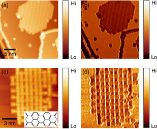
Fig. 7. (a) and (b) Simultaneously acquired high-resolution STM image and photon map over an area of 50 × 50 nm2 for H2TBPP molecules on Ag(111) (+2.5 V, 5 pA, 512 × 512 pixel, 0.98 ms/pixel). (c) and (d) Simultaneously acquired high-resolution STM image and photon map over an area of 12 × 12 nm2 for PTCDA molecules on Au(111) (−2.5 V, 200 pA, 307 × 307 pixel, 1.17 ms/pixel).
Download figure:
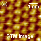
Standard image High-resolution imageHowever, for non-planar molecules such as spherical C60 molecules, the optical contrast on the molecular island may have different origin. Figure 8 shows one example of C60 monolayers on Au(111).72) The high resolution image enables us to correlate the topographic feature in Fig. 8(a) with the photon intensity distribution in Fig. 8(b). The C60 molecules appear darker in the photon map while the gap areas between the neighboring C60 molecules appear brighter. Figure 8(c) is an inverted photon map processed from Fig. 8(b). The contrast of the inverted image is very similar to the STM image in Fig. 8(a). The height undulations on the molecules is the dominant factor to yield molecularly resolved optical contrast in the photon mapping.72) Finally, we would like to end this section by noting that, thanks to the improvement in the optical collection and alignment (plus the assistance of a strongly emitting Ag tip), the molecularly resolved photon map in Fig. 7(b) was acquired using a small current of 5 pA and a short exposure time of 1.2 ms/pixel with a high pixel resolution of 512 × 512. Such mild photon mapping condition could be very important and helpful for mapping poorly conducting samples.
Download figure:
Standard image High-resolution image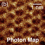
Download figure:
Standard image High-resolution image
Fig. 8. (a, b) High resolution images for STM topograph and simultaneously acquired photo map on a 1st-ML C60 island (+2.8 V, 800 pA, 5 × 5 nm2, 2.0 ms/pixel). (c) Inverted photon map processed from (b), showing very similar image contrast to the STM topograph in (a).72)
Download figure:
Standard image High-resolution image3.2.3. Spectroscopic imaging (or "color" photon mapping)
To date, the majority studies of photon mapping in STML experiments have focused on the spatial mapping of the total light intensity for each image pixel, while the spatially resolved fluorescence spectra are relatively limited.14,16–18,28,46,73) However, it is desirable to obtain the fluorescence spectrum simultaneously with topographic information at each pixel. This is because the spectroscopic imaging combines the advantage of both spectral measurements and intensity-based photon mapping and could provide a panoramic view of the spatial distribution of site- and specie-specific light emission properties. Such "color" photon maps can directly reveal the nature of optical transitions from various nanostructures on the surface, thus offering insights into the influence of local geometry, local electronic states and local environment on the observed light emission. In addition, if combined with Raman spectral measurements, such spectroscopic imaging can also enable a panoramic view of chemical identification and mapping of surface species at the nanoscale.
Figure 9 shows the schematics of the involved electronics control for the simultaneous acquisition of spectroscopic photon maps during the scanning of an STM image. Such "color" photon mapping is carried out through a synchronization function between the STM controller and CCD camera. For each pixel, the STM controller sends a transistor–transistor logic (TTL) pulse to trigger the CCD data acquisition. The spectral data are stored and processed in a separate optical personal computer (PC). Note that technically speaking, the synchronization procedure for spectroscopic imaging here is slightly more complicated than the intensity-based photon mapping described in the previous section. For an artifact-free spectroscopic imaging, one has to consider the relationship between the scanning speed (i.e., the time span on each pixel) and the integration time for each spectral measurement, taking into account the additional time required for CCD pixel grounding and data read-out and transfer time. Whereas in the intensity-based photon map, the optical signals from a photon counter are usually directly input into an auxiliary terminal in the STM controller and thus the signal synchronization is established automatically.

Fig. 9. Schematic diagram of electronics control for simultaneous acquisition of "color" spectroscopic mapping.
Download figure:
Standard image High-resolution imageFigure 10 shows one test example of such spectroscopic imaging on Ag(111).28) The step edge and the contaminants on the surface appear dark in the photon map while the flat Ag terrace appears bright. Such optical contrast can be easily supported by the fluorescence spectra simultaneously recorded on these three types of locations. As expected for plasmonic emissions from metal surfaces, the spectral profile remains essentially the same except for intensity variations. The relative peak intensity in these spectra exhibits strongly suppressed light emission on the step edge and contaminants, presumably owing to the local geometric effect on the field enhancement28,74) or the local electronic states for the probability of inelastic tunneling excitation.73) Spectroscopic imaging has been elegantly used to demonstrate atomic-scale optical contrast on Au(110)73) and Ag chains16) as well as sub-molecularly resolved optical contrast of HBDC molecules on Cu(111)14) and porphine molecules on oxidized NiAl surfaces.17,18) Such spectroscopic imaging data provide great insights into the nature of optical transitions and the origin of light intensity undulations and are expected to play more and more important roles in understanding STM induced light emission properties from quantum emitters such as molecules or quantum dots.

Download figure:
Standard image High-resolution image
Download figure:
Standard image High-resolution image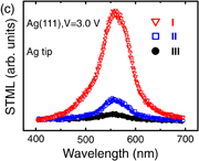
Fig. 10. (a) STM topograph of the Ag(111) surface (+3.0 V, 400 pA, 19 × 19 nm2). (b) Simultaneously acquired photon map with the photon intensity of each pixel integrated over 500–600 nm. (c) Typical STML spectra recorded at three different positions marked in (b): on the terrace (I), on the step (II), and on the protrusion (III) (+3.0 V, 400 pA, 300 ms). Reprinted from Ref. 28 with permission from American Institute of Physics.
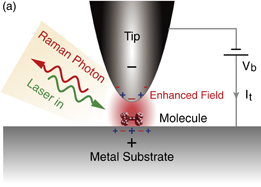
Download figure:
Standard image High-resolution imageWhile the fluorescence technique itself can offer certain chemical-specific information, it is well known that Raman spectroscopy is much more powerful in terms of providing chemical fingerprints of a molecular specie since each molecule has its own characteristic molecular vibrations. In the last part of this paper, we would like to mention very briefly our recent extension from STML to STM-controlled tip-enhanced Raman scattering (TERS) studies. The experimental setup is very similar to that shown in Fig. 9 except a laser beam is introduced into the STM junction for the Raman excitation and the signals detected are Raman scattered photons rather than fluorescence.20) By exploiting the confinement and enhancement of local plasmonic near fields produced by metallic nano-tips, the TERS technique offers combined advantages of both ultrahigh spatial resolution in scanning probe microscopy and sensitive chemical specificity in Raman scattering, and as a result, has wide applications in nanoscale chemical identification.7,75–80) As shown in Fig. 11, our recent development of a nonlinear STM-controlled TERS under a UHV–LT condition has pushed the spatial resolution below 1 nm at the sub-molecular scale, resolving the chemical identity and inner structure of a single H2TBPP molecule and even its orientation on the surface.20,81–84) Since TERS spectra is very sensitive to the molecular orientation due to surface selection rules, a small change in the orientation, as illustrated in Fig. 12 for a slightly more tilted H2TBPP molecule on Ag (compared with the molecule in Fig. 11), could change the relative intensity of Raman spectral peaks (but not positions) since only those Raman modes with components aligned parallel to the axial plasmonic field will be selectively enhanced. Note that for the eight Raman maps given in Fig. 12(b) with increasing wavenumbers, the characteristic four-lobe pattern of a H2TBPP molecule is clearly discernible in the TERS mapping at low wavenumbers (corresponding to low-energy vibrational modes). The molecular center appears dark while the lobes appear bright, although not so symmetric due to the tilting of the molecule on the surface. However, for relatively large wavenumbers above ∼1210 cm−1, the contrast and central dark area become smaller, which suggests more contributions from the vibrational modes of the central porphyrin core. As expected, if there is no noticeable Raman modes in the interested spectral range, the optical contrast should disappear in the Raman map, as evidenced in the TERS mapping on the far-right of Fig. 12(b).
Download figure:
Standard image High-resolution image
Fig. 11. (a) Schematic tunneling-controlled TERS in a confocal-type side-illumination configuration. (b) Representative TERS spectrum on the lobe of a flat-lying molecule on Ag(111). (c) Left: experimental TERS mapping of a single molecule processed from all individual TERS spectra acquired at each pixel for the 817-cm−1 Raman peak (120 mV, 1 nA, 0.3 s, image size: 3.6 × 3.6 nm2). Right: TERS intensity profile of the same line trace for the left Raman map, integrated over 800–852 cm−1.20)
Download figure:
Standard image High-resolution image
Fig. 12. (a) Single-molecule TERS spectra on the lobe (red) and centre (blue) of a slightly tilted H2TBPP molecule on Ag(111). The black spectrum is taken on bare Ag(111). (b) Experimental TERS mapping of a slightly tilted H2TBPP molecule for different Raman peaks (100 mV, 1 nA, 0.3 s). The wavenumber ranges for the intensity integration are indicated at the bottom.
Download figure:
Standard image High-resolution image
4. Conclusions
We have provided an overview of the instrumental development of a merged system of low-temperature UHV-STM with photon collection and detection capabilities. The crucial technical elements include invoking a large solid-angle coverage via an aspherical lens design for more efficient photon collection, a sophisticated in-situ lens control for better optical alignment, a fiber-free coupling directly onto sensitive single photon detectors to avoid the fiber-coupling loss, and a synchronization scheme for simultaneous spectroscopic imaging. We also use several selected examples (namely, luminescence spectra with good signal-to-noise ratios and optical imaging with sub-molecular resolution at low currents), not only to demonstrate the useful applications of the STML technique, but also to justify the excellent performance of our optimized optical-STM setup. The free-space light-coupling system can facilitate not only intensity-based photon mapping experiments, but also other modes of optical measurements such as isochromatic spectra,85) light polarization analysis,86) and even time-correlation measurements,87,88) upon the insertion of a filter, polarizer, or a beamsplitter in the optical path. The high photon signals achieved by the optical optimization also allow to carry out "color" spectroscopic imaging that is believed to play an ever-increasing role in the STML studies. Looking forward to the future, the combined system of the low-temperature UHV-STM with optimized optics could provide a powerful platform for exploring nanoscale optoelectronics on surfaces with ultrahigh spatial resolution and detection sensitivity, helping to gain insights into the nature of optical transitions, the behavior of dipolar coupling and plasmon-exciton coupling for energy transfer dynamics, and even the photon emission statistics for quantum light sources and quantum science. If the spectroscopic imaging is combined with Raman spectroscopy, the STM-controlled TERS technique has proven powerful for chemical identification and imaging at the sub-nm scale, which will open up avenues for probing and controlling materials at the single-molecule scale and is likely to trigger exciting activities in surface science and nanoscience, especially in surface chemistry and physics, photocatalysis, and even bio-molecular imaging.
Acknowledgments
We thank Dr. T. Nagamura at UNISOKU for discussion and technical support on the system instrumentation. This work was funded by National Basic Research Program of China, National Natural Science Foundation of China, and Chinese Academy of Sciences.