
Abstract
Theoretical calculation based on detailed balance and incorporating different realistic optical and electrical losses predicts conversion efficiency beyond 22% for single-junction perovskite devices. In dual-junction perovskite/silicon devices, theoretical conversion efficiency around 40% is been determined. However, dramatic drop in the conversion efficiency is shown to be due to the glass reflection and FTO parasitic absorption losses. Additionally, practical conversion efficiency limits of dual-junction two-terminal perovskite/silicon tandem solar cell of 30% are achievable as reported in this work using state-of-the-art demonstrated devices. Additionally, various crystalline silicon (industry and laboratory demonstrated) technologies are used as the bottom cell for the current matched tandem cell stacks with higher relative improvements when using commercial c-Si solar cells. Moreover, the effect of eliminating the parasitic resistances and enhancing the external radiative efficiency (ERE) in the perovskite junction on tandem performance are also investigated enhancing the stack efficiencies.
Export citation and abstract BibTeX RIS
1. Introduction
The silicon (Si) solar cell costs have reduced dramatically over the past few years that the entrenched, proven Si technology will likely remain the dominant photovoltaic (PV) technology over the coming decade. As the industry growth is stabilizing, cell conversion efficiency improvement (apart from the economies of scale in the past few years) will play a major role in cost reduction. The highest demonstrated Si cell efficiency of 25.6%1) (compared to a theoretical limit for Si of 29.4%2)) will provide a practical bound on what can be achieved commercially.
To progress the past incremental improvements in Si conversion efficiencies, it is necessary to consider a tandem approach whereby cells of different material (therefore with higher band-gaps) are stacked on top of Si. Stacking a single cell on top of Si will increase the theoretical limiting conversion efficiency from 29 to 42.5% while stacking two cells increases to 47.5%.3) The challenge has been to find cells of a similar inherent quality to Si that are suitable for such stacking.
The rapid emergence of cell technology based on organic–inorganic halide perovskite, a seeming disparate material system from Si, nonetheless has almost perfect complementarity in the properties required to form stacked cells on Si of high performance, see Fig. 1, due to its ease of fabrication, comparable absorption (direct band-gap material, high absorption coefficient and band-gap tunability) and electronic (low non-radiative recombination, long diffusion length and low exciton binding energy compared with organic materials) properties.4)
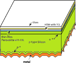
Fig. 1. Conceptual drawing of a likely perovskite/Si tandem cell structure with a thin-film perovskite cell fabricated on the Si cell.
Download figure:
Standard image High-resolution imageFirstly, simple deposition approaches can be used to prepare the perovskite either by one-step solution deposition,5) sequential solution deposition,6) thermal evaporation,7) vapour-assisted solution processing8) or hybrid chemical vapour deposition9) methods. Secondly, perovskite materials have comparable absorption properties with most of semiconductor materials that are used in high efficiency solar cell devices like having direct band-gap and high absorption coefficient (see Fig. 2). In addition, it has the advantage of band-gap tunability over the entire solar spectrum by mixing iodide with bromide or chloride10–13) or methylammonium cation (MA, CH3NH3+) with formamidinuim cation (FA, NH2CH=NH2+).14,15)
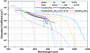
Fig. 2. Absorption coefficients of various semiconductor materials used for solar cell devices including four different perovskite materials: CH3NH3PbI3 (purple solid line), CH3NH3PbI3−xClx (blue solid line), CH3NH3Pb(I1−xBrx) with small bromide content (green solid line), and HC(NH2)2PbI3 (red solid line).
Download figure:
Standard image High-resolution imageLastly, perovskite has low non-radiative recombination (see Fig. 3 that shows the electroluminescent emission of various solar cell technologies at open circuit voltage), long diffusion length16) and low exciton binding energy17) compared with organic materials.
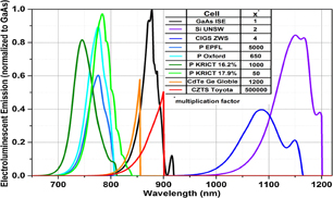
Fig. 3. The spectral luminescence for different solar cells on open circuit voltage normalized to the GaAs solar cell from Fraunhofer ISE.
Download figure:
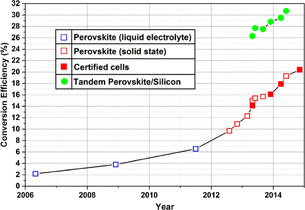
Standard image High-resolution imageThe first reported perovskite solar cell was based on liquid electrolyte with conversion efficiency of about 2% in 2006.18) By replacing the liquid electrolyte with solid hole conductor, the first high efficient solid state perovskite solar cell was reported in mid-2012 with efficiency above 14%.6) Since then, great attention has been paid to such solar cell technology resulting in rapid improvement in certified conversion efficiencies from 16.2% in end-201319) to 17.9% few month afterwards1) to the most recent 20.1%20) reported in November 2014.
In this work, the conversion efficiency limits of single-junction perovskite and dual-junction two-terminal perovskite/silicon tandem solar cell are calculated. For single-junction calculation, different optical and electrical losses are incorporated moving from the ideal conversion efficiency to the current state-of-the-art device. For dual-junction devices, both theoretical and presently demonstrated state-of-the-art calculations are shown.
2. Methods
One of the most auspicious approaches of assessing the upper efficiency limit of solar cell devices is via the detailed balance developed by Shockley–Queisser (SQ) in 1961.21) Unlike the semi-empirical efficiency approaches e.g.,22,23) where definite assumptions are made, e.g., material parameters, derivation of mathematical models employed and the incident light excitation, making the comparison to be made between them tricky, the SQ limit does not rely on optical and electronic properties that are not yet accurately determined for perovskite materials. That said, it is still possible to incorporate losses after the SQ limit is determined, such as incomplete absorption within the perovskite due to finite film thickness; front reflection from the glass; parasitic absorption loss within the transparent conducting film, i.e., fluorine doped tin oxide (FTO); and parasitic losses such as the series and shunt resistances. For optical generation within the perovskite material (A), two different schemes are investigated; planar device with two-pass [see Eq. (1a)] and textured with Lambertian light trapping [see Eq. (1b)]:24)

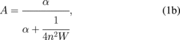
where α is the absorption coefficient, W is the thickness, and n is the refractive index. The reported absorption coefficient for CH3NH3PbI3 perovskite by Sun et al.25) is used. The refractive index is assumed to be 2.55 and fixed over all wavelengths.
For tandem perovskite/Si stack, the silicon sub-cell is assumed to have light trapping scheme with 300 µm thickness including Auger recombination beside the inevitable radiative losses. Tabulated values of refractive index reported by Green26) is used for the Si material.
3. Results and discussion
3.1. Single-junction perovskite solar cell
Figure 4 shows the conversion efficiency verses perovskite thickness using the two optical generation schemes. In the absence of optical losses, a conversion efficiency of above 31% is attainable even for a thin perovskite film 150 nm or above when the Lambertian light trapping is used. However a two-pass optical generation scheme requires a perovskite film thickness 10 times higher to achieve an efficiency of 31%. Efficiency limits drop to 28 and 24% when glass reflection and FTO parasitic absorption losses (using reported values by Wang et al.27)) are taken into account respectively. For these scenarios, thickness requirements do not change.
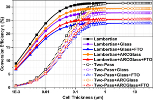
Fig. 4. The conversion efficiency of single-junction perovskite solar cell with Lambertian (solid lines with filled symbols) and two-pass (dotted lines with hollow symbols) optical generation schemes in the absence of optical losses (square markers); with normal glass reflection losses (purple lines circle markers); with normal glass reflection and FTO absorption losses (blue lines triangle markers). In addition, the efficiency is calculated having ARCTOP glass reflection losses (orange lines circle markers) and with ACTOP glass reflection and FTO absorption losses (red lines triangle markers).
Download figure:
Standard image High-resolution imageAs shown in Fig. 4, two of the most significant loss mechanisms are glass reflection and FTO parasitic absorption. Anti-reflective strategy can be used to reduce the former such as the deposition of quarter wavelength anti-reflecting coating and/or texturing of glass superstrate. A self-adhesive fluorinated polymer film (ARCTOP) on glass28) is evaluated in this work to investigate its impact on enhancing the conversion efficiency (see Fig. 4). Efficiency limits improve by 1.5% absolute compared with those when normal glass is used.
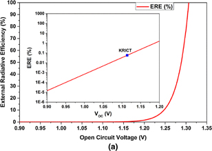
Figure 5 shows the conversion efficiency limit "waterfall" starting from detailed balance limit to the state-of-the-art perovskite solar cell efficiency i.e., 20.1% by the Korea Research Institute of Chemical Technology (KRICT).20) The upper limit for the perovskite material with a band-gap of around 1.55 eV is around 31.0%. The third and the fourth histograms show the drop in efficiencies due to finite perovskite thickness while the fifth and sixth histograms include losses due to glass reflection and FTO absorption. The second last histograms show the conversion efficiency of perovskite including non-ideal ideality factor of 1.5 which is within the range (between 1.3 and 2.029)) for most thin film solar cells. Including small parasitic resistances (Rs = 1 Ω cm2 and Rsh = 1000 Ω cm2), the perovskite solar cell efficiency will be around 21.0% which is very close to the latest certified result of 20.1% by KRICT whose cell has an estimated Rs of 1.55 Ω cm2; Rsh of 950 Ω cm2; and an ideality factor of 1.7.

Fig. 5. The conversion efficiency of single-junction perovskite solar cell using normal or ARCTOP glass after various losses.
Download figure:
Standard image High-resolution imageThe insignificant difference in conversion efficiency between the Lambertian light trapping scheme case and the two-pass scheme case illustrates the inconsequential impact from implementing light trapping in thin film perovskite solar cell. This is due to the high absorption coefficient in the perovskite semiconductor material.
After taking into account of reduced reflective losses from using the ARCTOP glass (violet and blue histograms), Fig. 5 shows that perovskite conversion efficiency of 22–23% are achievable for devices with acceptable parasitic resistances and typical ideality factor showing the importance of the use of anti-reflection.
3.2. Dual-junction two-terminal perovskite/Si stack
3.2.1. Theoretical calculation
As illustrated before, the losses associated with glass reflection and FTO parasitic absorption have significant effects on the photo-generated current and conversion efficiency. In the case where glass is used as part of an encapsulation scheme for the tandem cell covered by a transparent conductive layer, we can estimate the optical losses for the full wavelength range relevant to the perovskite top cell (300 to 800 nm) and Si bottom cell (300 to 1200 nm). This is performed by assuming the losses associated with the glass and transparent conductive layer which will be similar to that of a FTO glass. Figure 6 shows the measured transmittances of some of the typical FTO glasses such as FTO-TEC15, FTO-TEC9, FTO-TEC8, and FTO-TEC7 where the FTO sheet resistances are 15, 9, 8, and 7 Ω/□, respectively. Transmission degrades as FTO conductivity improves requiring a compromise for cell fabrication.
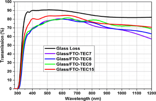
Fig. 6. Experimental transmission data for glass (black line), and FTO glasses FTO-TEC15 (red line), FTO-TEC9 (green line), FTO-TEC8 (blue line), and FTO-TEC7 (violet line).
Download figure:
Standard image High-resolution imageNote, the transmission data are underestimated since the measurement is done in air medium, i.e., air (n = 1)/glass (n = 1.55)/air (n = 1). It is expected to be higher in the presence of perovskite due to the graded refractive index such that air (n = 1)/glass (n = 1.55)/perovskite (n = 2.55) taking into account the absorption within the perovskite.
Figure 7 shows the short circuit current densities of the top junction perovskite (square symbols) and of the bottom junction silicon (circle symbols) without (blue lines) and with optical losses which are glass reflection (green lines) and glass/FTO losses (red lines). The corresponding dual-junction current matched efficiency limits (triangle symbols) are also shown. In this tandem calculation, light incident on the device experiences one-pass through the perovskite film while the transmitted light experiences Lambertian light trapping within the silicon wafer.

Fig. 7. The short circuit current density of perovskite (square symbols) and silicon (circle symbols) and tandem conversion efficiency (triangle symbols) as a function of perovskite thickness without losses (blue lines), with glass losses (green lines), and with glass/FTO losses (red lines).
Download figure:
Standard image High-resolution imageFigure 8 summarizes the expected perovskite/silicon tandem conversion efficiency of two-terminal current matched device. The first column shows the conversion efficiency without any losses. Efficiency of about 40.6% is expected with perovskite film thickness of 250 nm. A 5.6% absolute efficiency drop is expected from glass reflection alone. In addition, the required perovskite film thickness is less as the current required to match the current output of the Si cell is reduced due to the glass reflection affecting the entire wavelength range, in particular the operating wavelength range for Si cell.
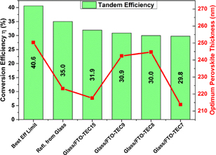
Fig. 8. The tandem conversion efficiency without optical losses, with glass reflection losses and on FTO/glass superstrates. The optimized perovskite thicknesses are also shown.
Download figure:
Standard image High-resolution imageThe tandem efficiency gets even lower when including the parasitic losses due to the FTO absorption. As conductivity of the FTO improves, tandem efficiency drops from 31.9% on a FTO-TEC15 superstrate to 29.8% on a FTO-TEC7 superstrate. The optimum perovskite film thickness to current matched with silicon varies with different FTO resistivities due to different absorption characteristics. FTO-TEC15 allows higher transmission over the operating wavelength range for the perovskite cell, hence requiring thinner perovskite film. Interestingly, FTO-TEC9 allows higher transmission over the operating wavelength range for the Si cell, hence requiring thicker perovskite film to match higher current output from Si cell. Finally FTO-TEC7 transmits the least amount over the Si cell operating wavelength range hence only requiring the thinnest perovskite film.
3.2.2. Calculation using demonstrated cell technologies
In this section, the practical conversion efficiency limits of dual-junction two-terminal perovskite/silicon tandem solar cell using state-of-the-art crystalline silicon (c-Si), industry and laboratory demonstrated, technologies as shown by blue histograms in Fig. 9 (where spectral response data are available) are investigated as the bottom cell for the current matched tandem. A perovskite cell with a certified conversion efficiency of 17.9% reported by KRICT1) is used as the top junction in this analysis.

Fig. 9. The conversion efficiencies of various silicon solar cell technologies (blue), and efficiency limits two-terminal perovskite/Si stack using demonstrated technologies (red) and efficiency limits of the two-terminal stack in the absence of parasitic resistance losses (green) under one sun AM1.5 G spectrum illumination.
Download figure:
Standard image High-resolution imageThe red histograms in Fig. 9 shows the maximum attainable efficiencies of perovskite/Si tandem cells under one sun AM1.5G illumination after the perovskite cell thicknesses have been optimized for current matching [see Fig. 10(a)]. Relative improvement of 43 and 18% is achievable for monolithically stacked thin-film perovskite on commercial screen printed (SP) and passivated emitter with rear locally diffused (PERL) c-Si solar cells respectively. The calculation suggests that a tandem stack that uses industrial silicon solar cell technologies such as PLUTO-passivated emitter rear cell (PERC), PLUTO-PERL and SunPower can achieve conversion efficiencies beyond that of the highest reported single-junction silicon solar cell. Tandem conversion efficiency above 28.0% is achievable using champion Si cells such as heterojunction with intrinsic thin layer (HIT); SunPower 25% and University of New South Wales (UNSW) PERL 25% cells. Interestingly, the HIT École Polytechnique Fédérale de Lausanne (EPFL) with relatively lower efficiency of 21.5% results in tandem conversion efficiency above 28.0%. This is because of its high spectral response at long wavelengths [see Fig. 10(b)] apart from its high open circuit voltage of 722 mV (comparable of that in SunPower 24.2% cell). Another interesting point to note is that although the Panasonic HIT 25.6% Si cell is more efficient than the UNSW PERL cell, the corresponding tandem efficiency is the same when either of them is used as bottom cell. This is due to the better current matching between Si and perovskite using the UNSW PERL cell because of the higher spectral response at long wavelengths compared with Panasonic HIT cell [see Fig. 10(b)].

Download figure:
Standard image High-resolution image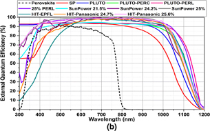
Fig. 10. (a) The short circuit current densities of top perovskite junction and various bottom silicon junction technologies as a function of perovskite thickness and (b) external quantum efficiencies under one sun AM1.5 G spectrum illumination of various bottom silicon junction technologies including top perovskite junction.
Download figure:
Standard image High-resolution imageGenerally, there are two main ways of further improving the tandem conversion efficiency. Firstly, by eliminating the parasitic resistances in the perovskite junction results in tandem stack efficiencies to exceed 26.0 and 32.0% on SP and UNSW PERL cells respectively as depicted by green histograms in Fig. 9. In fact, using most the silicon solar cell technologies, tandem efficiencies can exceed the Auger limit of single-junction silicon solar cell under one sun illumination i.e., 29.4%.
Secondly, by improving the external radiative efficiency (ERE) of the perovskite sub-cell and hence its open circuit voltage [see Fig. 11(a)], the tandem performance enhances. Here the effect of perovskite cell's ERE on the tandem performance is investigated using industrial SP and UNSW PERL cells. Figure 11(b) shows the tandem conversion efficiency versus top perovskite ERE with (solid lines) and without (dashed lines) parasitic resistances in the perovskite. For perovskite/SP Si stack [see blue lines in Fig. 11(b)], ERE of above 2% is required for tandem conversion efficiency to exceed the 25%. Excluding the parasitic resistance from the perovskite relaxes the demand for ERE, only 3 × 10⁻³% of ERE is needed to overcome the 25% efficiency. Same observations are seen for the perovskite/PERL Si stack [see red lines in Fig. 11(b)] where ERE of 0.2 and 4 × 10⁻⁴% are required to exceed the 30% conversion efficiency with and without parasitic resistances, respectively.
Download figure:
Standard image High-resolution image
Fig. 11. The effect of the perovskite ERE on (a) the open circuit of the perovskite sub-cell and (b) the tandem conversion efficiency with commercial SP (blue lines) and UNSW PERL c-Si (red lines) solar cells with (solid lines) and without (dashed lines) parasitic resistances in top perovskite junction.
Download figure:
Standard image High-resolution imagePushing the perovskite conversion efficiency closer to a realistic 20% having JSC = 22 mA/cm2, VOC = 1.1 V, and FF = 80%, tandem conversion efficiency close to 32% is theoretically achievable when combined with the UNSW PERL c-Si (see Fig. 12). Stacking the more recent perovskite efficiency of 19.3% with published data,30) even it is not certified, yield tandem device efficiency around 31%.
Fig. 12. The correlation between the tandem cell conversion efficiency (green circles) and perovskite cell conversion efficiency (red squares) is shown.
Download figure:
Standard image High-resolution image
4. Conclusions
The ability of fabricating high efficient perovskite solar cell devices by several means of relatively cheap deposition methods opens opportunities for low cost thin film organic inorganic solar cells as well as tandem solar cell technology using the incumbent low cost Si substrates. The effect of optical losses associated with glass reflection and transparent conductive layer absorption and the effect of electrical losses from parasitic resistances and recombination on tandem cell efficiency have been analyzed. Practical tandem efficiency limits of 30% are achievable as reported in this work. Pathways for further tandem efficiency improvements as a result of minimizing parasitic losses and improved external radiative efficiency of the perovskite cell are also investigated in this work.
Acknowledgments
This work was supported by the Australian Government through the Australian Renewable Energy Agency (ARENA). Responsibility for the views, information or advice expressed herein is not accepted by the Australian Government. One of the authors, I. Almansouri, would like to express his gratitude to Masdar Institute for funding his Ph.D. studies at the UNSW under the Masdar Institute Fellowship Program.