Abstract
The aim of this paper is to summarize considerable experimental efforts undertaken within the last decades in the investigations of transport properties of β-FeSi2. The β-FeSi2 compound is the most investigated among a family of semiconducting silicides. This material has received considerable attention as an attractive material for optoelectronic, photonics, photovoltaics and thermoelectric applications. Previous reviews of the transport properties of β-FeSi2 have been given by Lange and Ivanenko et al. about 15 years ago. The Hall effect, the conductivity, the mobility and the magnetoresistance data are presented. Main attention is paid to the discussion of the impurity (defect) band conductivity, the anomalous Hall effect, the scattering mechanisms of charge carriers, as well as to the hopping conduction and the magnetoresistance.
Export citation and abstract BibTeX RIS
1. Introduction
Semiconducting iron disilicide or β-FeSi2 is a promising compound for optoelectronic devices on Si substrates, photonics, photovoltaics, and is attractive for high-temperature thermoelectric materials.1–3) Because of its high optical absorption coefficient (exceeding 105 cm−1 at 1.0 eV) and abundant element resources in the Earth's crust, β-FeSi2 is expected to be a promising photovoltaic material4–6) with a theoretical energy conversion efficiency of about 16–23%.4,5) The direct band gap of 0.83–0.87 eV (Refs. 1, 2, and 7) provides a potential applicability for light emitting diodes and optical sensors operating at wavelength of about 1500 nm relevant to the quartz optical fiber telecommunication. In addition, β-FeSi2 has a high refractive index exceeding 5.6 in the transparent range.1,2) Possible application of high refractive semiconducting silicides to high index contrast photonic crystals has been proposed.8,9) Reports on electroluminescence at 1.5–1.6 µm,10,11) strong photoluminescence at 1.54 µm,12) as well as publications on advanced β-FeSi2 based materials as rodlike,13) nanodots,14,15) nanowires,16,17) and nanocomposites18,19) increase possibilities of the β-iron disilicide utilizations.
This review is devoted to discussion of transport properties of n- and p-type β-FeSi2 crystals and films. Main attention is paid to the Hall effect data, especially to the impurity (defect) band conductivity in p-type and to the anomalous Hall effect strongly pronounced in n-type crystals and films, as well as to observations and analysis of the Mott- and Shklovskii–Efros variable range hopping conductivity. The scattering mechanisms in the β-FeSi2 crystals and films and the magnetoresistance data are also discussed.
2. Impurity (defect) band conduction
The p-type undoped20,21) and Cr-doped β-FeSi2 single crystals [Fig. 1(a)] and films,22) the single crystals, both Al-doped23) and grown from Zn solvent [Fig. 1(b)],24) as well as the β-Fe1−xMnxSi2 alloys25) show an exponential increase of the Hall coefficient R(T) with decreasing temperature T down to ∼50–170 K. In addition, it should be mentioned a well-pronounced maximum of R(T), which implies importance of the conductivity over a band formed by shallow impurity (or defect) levels. When the concentration of shallow impurities is increased, the magnitude of the Hall coefficient maximum decreases strongly and its position shifts towards higher temperatures. In the heavily doped sample the maximum of R(T) vanishes.

Download figure:
Standard image High-resolution image
Fig. 1. (a) Temperature dependence of the Hall coefficient in the Cr-doped p-type β-FeSi2 samples.22) The numbers of the curves correspond to the sample numbers (Table I). (b) Temperature dependence of the Hall coefficient in the p-type β-FeSi2 crystals grown from Ga and Zn solvents.24) The numbers of the curves correspond to the sample numbers (Table I).
Download figure:
Standard image High-resolution imageHowever, it is worth mentioning that the value of Rf or the smallest value of R(T) at low temperatures (where pf = 1/eRf is the concentration of the impurity band holes in the carrier freezing region) is much smaller than that of Rd, which corresponds to depletion of the impurity states at the highest temperatures. This feature cannot be explained by assuming a two-band model (including the valence and the impurity bands) only, but suggests the existence of an additional deep acceptor level.23)
Explicit analysis of the Hall effect under assumption of existing two acceptor levels and a single donor level has been performed in Ref. 23 with the equation
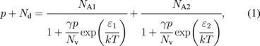
where p is the concentrations of free holes, NA1 and NA2 is the concentration of the shallow and the deep acceptors with energies ε1 and ε2, respectively, Nv = 2(2πm*kT/h)3/2 is the density of states in the valence band, γ = 2 is the degeneracy factor and Nd is the concentration of the compensating donors.23) This permitted determination of the parameters ε1, ε2, NA1, NA2, and Nd in the Al-doped p-type β-FeSi2 single crystals (see Table I). The same model was applied also to the analysis of R(T) in the β-FeSi2 single crystals doped with Cr (Ref. 22) and Mn (Ref. 25), yielding, however, less confident data (Table I). The values of ε2, Nd, and NA2 were obtained for the β-FeSi2 crystals grown from Zn solvent (see Table I).24) However, it should be emphasized that Eq. (1) is valid only for local levels characterized by negligible overlap of the impurity states. It can be applied for impurity bands as well, until they are narrow enough. On the other hand, the obtained high values of NA1 and especially NA2 in Table I are not in line with the latter statement, meaning that rather a band approximation (or continuous density of states in the impurity band) should be used instead of the system of local levels given by Eq. (1). Therefore, the data in Table I should be regarded only as estimates.
Table I. Parameters of p-type β-FeSi2.
| Sample No. | NA1 (1016 cm−3) | NA2 (1019 cm−3) | Nd (1019 cm−3) | ε1 (meV) | ε2 (meV) |
|---|---|---|---|---|---|
| 8 (undoped)21) | 1.45 | 0.174 | 6.1 | 68 | 123 |
| 6 (Al-doped)23) | 0.36 | 3.7 | 1.4 | 48 | 93 |
| 3 (Al-doped)23) | 2.8 | 14 | 6.9 | 50 | 103 |
| 1 (Al-doped)23) | 2.1 | 87 | |||
| 7a) (Cr-doped)22) | 223 | 128 | 470 | 31 | 94 |
| 8a) (Cr-doped)22) | 980 | 388 | 5 | 93 | |
| 9a) (Cr-doped)22) | 2900 | 360 | 6 | 91 | |
| 10 (Cr-doped)22) | 1 | 13 | 8 | 30 | 85 |
| Zn10-124) | 0.11 | 117 | |||
| Zn10-224) | 0.12 | 123 | |||
| Zn1324) | 0.41 | 121 | |||
| Zn2124) | 0.042 | 121 | |||
| 1 (Mn-doped)25) | 44.8 | 41 | 36.2 | 135 | 299 |
| 3 (Mn-doped)25) | 17.7 | 53 | 9.4 | 116 | 258 |
| Ga424) | 5.4 | 2400 | 17 | ||
| Ga624) | 4.8 | 1500 | 18 | ||
| Ga224) | 4.2 | 1400 | 18 |
a) Films.
The R(T) function of the p-type β-FeSi2 single crystals, grown from Ga solvent,24) shows an exponential increase with decreasing the temperature. The values of NA1, Nd, and ε1 (Table I) have been determined by numerical simulations of the temperature dependence of the hole concentration.24) Their estimative character also follows from the application of Eq. (1) reduced to a single acceptor level.24)
The results above, as well as those published earlier, which have been obtained in undoped26–30) and differently doped (V, Cr, Mn, Pd, Ni,31) Co,30,32) and Al23,32)) material, demonstrate the existence of the deep levels with energies lying between ∼80–160 meV. These levels, however, can be connected not only to doping elements, but also to uncontrolled impurities and/or native defects.21) Single crystals grown from Ga solvent show relatively shallow levels of about 18 meV,24) while the deepest levels are observed in the Mn-doped crystals (260–300 meV).33–35)
3. Anomalous Hall effect
3.1. P-type β-FeSi2
A nonlinear dependence of the Hall voltage on the magnetic field was reported for undoped p-type films and Cr- and Mn-doped single crystals. It was found, that these samples were usually those grown with starting materials of a poor purity.36) However, the nonlinear field dependence of the Hall resistivity was reported also for the p-type Mn-doped β-FeSi2 single crystals grown from high purity elements.37)
Manganese is one of the most effective doping elements for β-FeSi2 used as a thermoelectric material.33) Several studies were performed on polycrystalline alloys of β-Fe1−xMnxSi2 with x = 0.01–0.1, and their transport properties were investigated at T = 77–1200 K.34,35) The results of the transport measurements between T = 80 and 300 K were explained assuming the existence of the impurity band. The corresponding activation energies of the shallow (90–135 meV) and deep acceptor levels (220–300 meV) were estimated.24)
The magnetic field dependences of the magnetization, M, and the Hall resistivity, ρH, of the Mn-doped β-FeSi2 single crystals,37) presented in Fig. 2, are similar to those observed in ferromagnetic (FM) semiconductors.38) Observations of the remanence and hysteretic effects may indicate a FM ordering. However, the magnetic irreversibility increasing on cooling, as well as absence of saturation of the magnetization37) resemble rather the behavior pertinent of spin glasses.39)

Download figure:
Standard image High-resolution image
Fig. 2. (a) Plots of the magnetization vs magnetic field for Mn-doped β-FeSi2 single crystal (with 2 wt % of Mn) at different temperatures.37) The hysteresis curve at 20 K is shown in the inset. (b) Dependence of the Hall resistivity on the magnetic field for the same sample.37)
Download figure:
Standard image High-resolution imageThe Hall resistivity in a FM material follows usually a phenomenological relation

where B = H + 4πM is the magnetic induction, M is the magnetization of the sample, Ro and Ra are the ordinary and anomalous Hall coefficients, respectively.40) The anomalous Hall effect (AHE) is not restricted to ferromagnetic materials only, but can occur also in materials containing large localized magnetic moments. AHE arises from asymmetric scattering of charge carriers by various irregularities in a regular arrangement of the localized moments of magnetic ions. The sign of Ra depends on the type of scattering centers and may be positive or negative for both electrons and holes.41)
Assuming that Ro and Ra do not depend on the magnetic field, the value of RaMs and the saturation magnetization Ms have been determined with a linear extrapolation of the Hall resistivity and the magnetization, respectively, to zero magnetic field. The importance of the anomalous contribution to the Hall resistivity has been found in the samples studied, especially at low temperatures. The value of Ra increases strongly with decreasing the temperature (from ∼0.01 to 1 Ω·cm/G in the range of 300–50 K for #20 with 1 wt % of Mn and from 0.5 to 25 Ω·cm/G in the range of 300–150 K for #39 with 2 wt % of Mn).
Equation (2) can be written in the following form:
where σ0 is the conductivity in zero magnetic field and σH is the coefficient, which defines the Hall effect in the approximation that the current components vary linearly with field H.38) The temperature dependence of Ra (i.e.,  ) should behave as the inverse of the square of the electrical conductivity, because
  is expected to be sensitive only to such temperature-independent parameters as the relevant spin–orbit coupling, the exchange interaction between the free carriers and the localized magnetic moments, as well the low-temperature scattering mechanisms. The parameter
  provides some measure of the effectiveness of the microscopic processes, which lead to an asymmetric (skew) scattering generating the AHE.
In the single crystals above, the dependence of Ra ∼ ρn has been found, where n = 2.2 ± 0.2. The obtained values of n are in a reasonable agreement with that (n = 2) predicted by Eq. (3) for FM materials, as well as by Gurevich and Yassievich42) for the case of metals with a center of inversion and dominant scattering by phonons. The structure of β-FeSi2 contains the center of inversion, and the phonon scattering is found to be an important scattering mechanism. Although the samples studied are semiconductors, the model of Gurevich and Yassievich42) (developed for metals) describes the AHE satisfactorily, whereas such relations as Ra ∼ ρ, Ra ∼ ρ/μT, or  have not been observed.
The temperature dependence of the ordinary Hall coefficient Ro(T) ∝ 1/p of Mn-doped β-FeSi2 single crystals shows an exponential increase with decreasing the temperature. The data have been analyzed assuming one acceptor level with the energy ε and one donor level.23) The value of ε = 244 meV, as well as the acceptor concentration NA = 3.3 × 1019 cm−3 have been determined in a good agreement with the corresponding data obtained in β-Fe1−xMnxSi2.25,34)
3.2. N-type β-FeSi2
All n-type β-FeSi2 single crystals grown by chemical vapor transport (CVT), both undoped and differently doped, show the nonlinear magnetic field dependence36,43,44) and hysteresis36,45) of the Hall voltage. The nonlinearity is strongly pronounced at low temperatures and is observed even at room temperature (RT). The hysteresis vanishes at T ∼ 100–150 K. These peculiarities can be ascribed to a FM nature of the investigated material (or to presence of large magnetic moments), giving rise to the AHE, and/or to the presence of two types of carriers, the light and the heavy electrons.
First observation of the AHE in β-FeSi2 was reported in Ref. 43. It was found, that the magnetization was an almost linear function of H at temperatures around and above RT in magnetic fields up to H = 8000 Oe, and deviated from the linearity at lower temperatures (Fig. 3). The values of M were quite small (less than 0.05 G). It is known, that the anomalous Hall effect is strongly dominated in FM metals, where R can be up to 2 to 3 orders of the magnitude higher than the normal Hall constant, but is much less pronounced in other materials. Taking into account the experimental data of M, it was found that the values of the ratio RaM/R0B did not exceed ∼10−2–10−3 in the samples studied. This permits to neglect the second term in Eq. (7). The contribution of the AHE to the total Hall voltage is negligible in the samples studied, and no evidence of a FM phase transition around 100 K has been detected. Moreover, the neutron scattering experiments, as well as the electron paramagnetic resonance measurements, gave no evidence for the existence of a FM order.2)

Fig. 3. Magnetization vs magnetic field for Al-doped p-type β-FeSi2 single crystal.43)
Download figure:
Standard image High-resolution imageTherefore, the observed variation of R with H is attributable to the magnetic field dependence of the normal Hall coefficient within the whole investigated temperature range. The Hall coefficient exhibits a strong decrease with increasing magnetic field (Fig. 4). This cannot be explained within the limits of the one-band conductivity model and should be ascribed to the presence of two types of charge carriers. With the two-band conductivity model, parameters of the light and heavy electrons, as well as the separation between the two bands, have been estimated. The data are in agreement with the band structure calculations of β-FeSi2,46) predicting two groups of electrons, the light ones at the Y point of the Brillouin zone with the effective mass of 0.49m0 (where m0 is the free-electron mass), and the heavy electrons with a much higher effective mass at the L point, the energetic separation between the two valleys being 8 meV.

Fig. 4. Plots of the Hall coefficient vs magnetic field for the Al-doped p-type β-FeSi2 single crystal. The solid lines are evaluated using the expression for the two-band Hall coefficient proposed by Chambers (from Ref. 43).
Download figure:
Standard image High-resolution imageHowever, recent experiments on β-FeSi2 crystals indicate that the observed small FM contribution to the magnetization, relaxation of the remanent magnetization and the anomalous contribution to the Hall resistivity can be caused by inhomogeneities of the samples.36,47) The assumption of superparamagnetic clusters can explain important details of the experimental observations. Superparamagnetism is characterized by a relaxation of the remanent magnetization, which is increased on heating. With increasing temperature, the number of the stable superparamagnetic clusters is increased. This explains the gradual decrease of the strength of nonlinear effects in the ρH(B) dependence.36,47)
The magnetic properties of the n-type β-FeSi2 single crystals were investigated using measurements of the magnetization and the AHE. The data show the appearance of superparamagnetic inclusions, which origin is attributed to defect-induced magnetic aggregates. The schematic image of them is displayed in the inset of Fig. 5, where the Fe-rich aggregates (AG) or clusters built of magnetic atoms are distributed randomly in the sample. It is also possible, that isolated spins are distributed randomly, but a detailed analysis reveals no single spins but magnetic aggregates composed of 400–1300 spins. Therefore, the hysteresis of M(H) is attributed to the interaction between the magnetic aggregates. Absence of the interaction gives rise to the M–H curve without hysteresis: the former and the latter are the cases at 4.2 and 150 K, respectively, as shown in Fig. 5.47)

Fig. 5. Plots of M vs H in the n-type β-FeSi2 single crystal at 4.2 K (1, black data) and 150 K (2, green data). Inset: The image of the superparamagnetic clusters (schematically), where F-AG means the clusters built of magnetic atoms and distributed randomly in a sample.47)
Download figure:
Standard image High-resolution imageAt higher temperatures, just below a peritectic decomposition temperature, β-FeSi2 should have some homogeneity range. Therefore, this semiconductor is of the n-type on the Fe side of this range and of the p-type on the Si side. Such behavior looks similar to many other semiconductors (e.g., Bi2Te3, GaAs, and those of the group II–VI). The range of the homogeneity narrows on cooling. The compositions of FeSi2+x or Fe1+xSi2 become metastable leading to the Fe-rich precipitates. The precipitation requires a nucleation, where a nucleus should be composed of a few atoms. Similar precipitation should be formed from a p-type material, but the precipitates will be the Si-rich aggregates. These may be determined only by some structural analyses, because electrically such aggregates can be neutral. This permits to explain, why the AHE is strongly pronounced in the n-type β-FeSi2. It is worth mentioning, that the β-FeSi2 crystals grown by CVD are crystallizes at high temperatures, where the homogeneity range is wide. Therefore, on cooling the crystals decompose into FeSi2 with a narrow homogeneity range, having Fe on one side and Si on the other side.
N-type β-FeSi2 single crystals were also grown using Sn-,48) Sb-,49) and Ni-doped Zn solvent50) at temperatures even higher (∼850–900 °C) that those used for CVT growth (∼750–850 °C). That is why, we can assume appearance of anomalies similar to those reported for crystals grown by the CVT method. The temperature dependences of the electron concentration show a steep decrease down to ∼100 K and a much weaker decrease down to ∼10–20 K in the case of Sb solvent, as well as a tendency to saturation for the β-FeSi2 crystals grown from Sn solvent. Only the high-temperature region was analyzed, where the values of the energy of donor levels were estimated (∼0.11–0.12 eV). A much lower activation energy (∼26–60 meV) was reported for the Ni-doped n-type β-FeSi2 single crystals. The Hall measurements were performed only at B = 0.35 T. No magnetic field dependence of the Hall voltage was reported. Therefore, it is not clear whether the AHE takes place or not in the samples grown by solution methods. A more detailed study is required to clarify this issue.
It is difficult to separate the influence of the two-band conduction and the superparamagnetism effects. For this purpose, we should grow the n-type β-FeSi2 crystals without Fe precipitates. To achieve them, we should probably find a way to grow crystals at temperatures below those used at present time by CVT (the growth temperature Tg is ∼750–850 °C),51,52) the solution methods using the Sn solvent (Tg = 880 °C)48) or the Sb solvent (Tg = 850 °C)49) and the molten salt method (thermal treatment at a temperature of 900 °C).53,54)
4. Scattering mechanisms of charge carriers
Investigations of the scattering mechanisms are rare, and the obtained results are not in conformity with one another.
According to Dimitriadis et al.,29) the mobility of β-FeSi2 thin films follow in the range of ∼100–300 K the relation of μ ∝ T−n, where n = 1.5 indicates importance of the acoustic phonon scattering. Regoliny et al.27) studied thin films grown at 750 °C (LT) and 850 °C (HT). The dependence of μ ∝ T−3/2 corresponding to the acoustic phonon scattering was observed only for the HT samples. The mobility of the LT samples exhibited the law μ ∝ T−1. Oostra et al.26) have reported, that the mobility follows the behavior of μ ∝ T−1.9 instead of T−3/2 as expected for the acoustic phonon scattering below RT, whereas the scattering mechanisms other than a simple intra-valley acoustic phonon scattering are important in the β-FeSi2 thin films studied.
The high values of n have been also reported for the undoped (n = 3.6) and the Cr-doped (n up to 2.4)44) β-FeSi2 single crystals.23) Availability of high quality β-FeSi2 single crystals, both undoped44) and Al-doped,23) permits to get a more reliable data on the scattering mechanisms in the investigated material.
It is worth mentioning some correlation between the values of n and μ, which is known as an indication of quality of the material. The reported value of n varied from ≈1 in the low hole mobility samples (μmax = 20 cm2·V−1·s−1 at 77 K28)) up to 3.6 in the high hole mobility samples (μmax = 1200 cm2·V−1·s−1 at 74 K;21,23) 490 cm2·V−1·s−1 at 120 K44)). A correlation between the value of n and the purity of the starting materials was mentioned by Brehme et al.44)
To estimate strength of different scattering mechanisms, the total mobility can be calculated in the Mathiessen approximation,

where μac, μnpo, μpo, and μi are the mobilities of the charge carriers due to scattering by acoustic lattice modes,55) nonpolar optical modes,55,56) polar optical modes,57) and ionized impurities,58) respectively. The details of the terms entering Eq. (4) can be found in Refs. 56 and 57.
Analysis of the mobility data with Eq. (4) has been performed in Ref. 21 (an example is shown in Fig. 6). The values of the acoustic deformation potential constant, Eac = 3 eV (at p = 1017 cm−3 and T = 300 K) and Eac = 5 eV (at p = 1018 cm−3 and T = 300 K) have been obtained with the fitting of the experimental data. The observed increase of Eac with increasing the hole concentration can be caused by neglect of the hole–hole scattering contribution. The discrepancies in the values of the mobility in β-FeSi2 single crystals at 300 K (10–40 cm2·V−1·s−1),3) which should not take place at a pure lattice scattering, can be associated also with the additional hole–hole scattering contribution.

Fig. 6. Temperature dependences of the calculated partial mobilities (dashed lines) and the total mobility (solid line) for the undoped β-FeSi2 single crystal. The squares are the experimental mobility data.21)
Download figure:
Standard image High-resolution imageIn the samples studied, scattering due to the polar optical phonons and nonpolar optical phonons is the most important at temperatures, lying between ∼80–150 and 300 K (Fig. 6). The calculated contribution due to scattering by ionized impurities was found to be negligible within this temperature region.
In the case of Cr-doped β-FeSi2 single crystals, scattering due to space charge regions has been also taken into account. It has been found, that scattering due to the polar optical phonons and nonpolar optical phonons is the most important at temperatures between 100 and 300 K. Scatterings due to the ionized impurities and the space charge regions are most effective at lowest temperatures, whereas scattering due to the space charge regions dominates in all samples studied in the low-temperature region.59) The latter can be connected with presence of a deep acceptor level, distributed inhomogeneously.60)
Scattering mechanisms in the β-FeSi2 thin films were discussed in Refs. 61 and 62 (see Fig. 7). Not intentionally doped p-type β-FeSi2 thin films were grown on Si(111) substrates by molecular-beam epitaxy using the low-purity (4N) and high-purity (5N) Fe sources. This was done to investigate the effect of a high-purity Fe source on the electrical properties of β-FeSi2. The hole mobility increased and the hole density decreased considerably as the annealing temperature and time were increased, particularly for the β-FeSi2 films produced with 5N-Fe. The observed temperature dependence of the hole mobility was analyzed by similar way as for single crystals, and was reproduced well by considering scatterings by the acoustic, polar and non-polar optical phonons and by the ionized impurities.61)

Fig. 7. Plots of the calculated partial mobilities and the total mobility, μtot, vs temperature, for the undoped p-type β-FeSi2 film. The triangles are the experimental mobility values.61)
Download figure:
Standard image High-resolution imageThe analysis shows, that the ionized impurity or acoustic-phonon scatterings become predominant at low temperatures, whereas the optical-phonon scattering dominates at high temperatures. The higher hole mobility in the β-FeSi2 films formed with 5N-Fe was attributed to a reduction of the ionized impurity scattering. The value of Eac was decreased from 55 to 7 eV with increasing the annealing temperature and time. This was considered to reflect the improvements of the crystal quality of β-FeSi2. It is worth mentioning, that Eac is lower in single crystal, lying between ∼7–8 eV in Cr doped22) and between ∼3–5 eV in undoped material.21)
The highest reported hole mobility value in single crystals is 1200 cm2·V−1·s−1 at 74 K,23) whereas the room temperature values are ∼20–40 cm2·V−1·s−1. The β-FeSi2 thin films, epitaxially grown on a Si substrate and annealed, show the hole mobility up to ∼100–450 cm2·V−1·s−1 at 300 K,61,62) increasing up to ∼13000 cm2·V−1·s−1 at 50 K.62) The highest electron mobility is ∼200–400 cm2·V−1·s−1 at room temperatures, increasing up to 14800 cm2·V−1·s−1 at 70 K.63)
The value of the charge carrier mobility is considered to be one of the most important parameters characterizing the quality of the materials studied. Can the difference of the mobility values, constituting an order of the magnitude in films and single crystals, be due to a higher quality of epitaxially grown films with respect to single crystals, or due to some influence of substrate in transport studies? This possibility has been discussed by Brehme et al.65) and cannot be excluded from consideration.
5. Hopping conductivity
When the temperature is decreased, the band conductivity of doped semiconductors becomes ineffective due to an exponentially low concentration of charge carriers, activated from impurity levels into the conduction or valence band. Then, the hopping conductivity sets in, which is connected with a charge transfer over localized states of an impurity band.65) The resistivity of weakly doped semiconductors in the domain of the hopping conduction is given by a universal law,
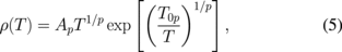
where Ap is a prefactor constant and p = 1, 4 (three-dimensional hopping, 3D) or 3 (two-dimensional hopping, 2D) and 2 for hopping only over the nearest neighboring centers, for the Mott (depending on the dimensionality of a system) and the Shklovskii–Efros (SE) variable-range hopping (VRH) conduction regimes, respectively.65,66) Here, T0p is the characteristic temperature depending on the hopping conduction mechanism.65,66) Generally, transition to the VRH conductivity takes place with lowering the temperature or increasing a microscopic disorder, when it is energetically favorable for a carrier to jump beyond the nearest neighboring impurity centers.65,66) In particular, the Mott type of VRH dominates, when Coulomb interactions between the charge carriers are unimportant.66) Otherwise, such interactions lead to formation of a soft Coulomb gap with width Δ in the density of the localized states (DOS) around the Fermi energy, EF, and the SE VRH regime sets in.65) The value of T0p is determined by the DOS value at EF, g(EF), for the Mott VRH mechanism (when the DOS around EF is constant) or by the DOS outside the Coulomb gap, g0, for the SE mechanism (where the DOS is zero at EF), as well as by the values of the localization radius, ξ, and the dielectric permittivity, κ.65,66) Therefore, such parameters as Δ, W (the width of the impurity band), g(EF) or g0, ξ, and κ can be obtained or estimated with a detailed analysis of the dependence of ρ(T) in the corresponding VRH intervals. It should be emphasized also, that the parameters ξ, κ, Δ, and DOS are quite sensitive to proximity of an impurity system to the Anderson metal–insulator transition (MIT).65,66) Therefore, T0p is sensitive to the proximity to the MIT, too, decreasing when the concentration of impurities approximates a critical concentration of the MIT, Nc.66)
As can be seen in Fig. 8, broad intervals of the Mott VRH conduction have been established in β-FeSi2 polycrystalline films.67,68) The values of T04 = (4.3–32) × 103 K and ξ = 74–105 Å [assuming g(EF) = 1031 erg−1 cm−3 ≈ 1.6 × 10¹⁹ meV−1 cm−3] at the defect concentration Nd = (2.4–20) × 1018 cm−3 have been found in Ref. 67 for samples A–D in Fig. 8(a) (the type of the conductivity has not been determined). It has been found also, that the film thickness exceeds the optimum hopping length, corresponding to the 3D hopping in agreement with Eq. (5) and remarks below. On the other hand, the values of T04 = (1.2–0.83) × 106 K obtained in Ref. 68 for the p-type β-FeSi2 films, annealed at temperatures Tann = 600–800 °C [Fig. 8(b)] are much higher than those in Ref. 67. Such a difference of T04 suggests that the films in Ref. 67 are closer to the MIT. Enhancement of the resistivity values in Ref. 68 with respect to Ref. 67 agrees with such a conjecture. Strong decrease of g(EF) = (280–1.1) × 1019 meV−1·cm−3 with increasing Tann has been reported.68) However, the mean hopping length, Rhop (100 K) = 1.5–5.9 Å,68) is smaller than the lattice parameters of β-FeSi2 (Refs. 1 and 2).

Download figure:
Standard image High-resolution image
Fig. 8. Plots of (a) the resistivity67) and (b) the conductivity68) vs T−1/4 in polycrystalline β-FeSi2 thin films [in (b) are given the annealing temperatures of the films].68)
Download figure:
Standard image High-resolution imageAs follows from Fig. 9, both VRH regimes are observed in the p-type β-FeSi2 single crystals doped with Al, with the onsets below ∼40 and 4.5 K for the Mott and the SE VRH conduction, respectively.69) Note, that in Ref. 69 the symbol "log" in Fig. 9 was confused with the symbol "ln", which is correct here. Analysis of the ρ(T) data permits to obtain the values of g(EF) ≈ (0.5–3.7) × 1015 meV−1·cm−3 in the Mott VRH regime, which are quite comparable with those of g0 ≈ (0.4–1.3) × 1015 meV−1·cm−3, obtained in the SE regime, as well as with the calculated DOS values near EF,65) gcalc ≈ (0.9–2.3) × 1015 meV−1·cm−3.69) In sample #5,69) both VRH conduction regimes are observed in different temperature intervals (Fig. 9). This permits to compare the values of the microscopic parameters, obtained in each VRH regime in the same sample: g(EF) ≈ 0.5 × 10¹⁵ meV−1·cm−3 and g0 ≈ 1.3 × 10¹⁵ meV−1·cm−3, both being close to gcalc ≈ 0.9 × 10¹⁵ meV−1·cm−3; ξ ≈ 700 and 1000 Å in the Mott and the SE VRH conduction regimes, respectively.69) In addition, the increase of ξ ≈ 660–1900 Å and κ ≈ 27–170 with increasing NA between 3.6 and 8.4 (in units of 1015 cm−3) has been found.69) Eventually, the values of Δ ≈ 0.49 and 0.27 meV have been obtained, which together with the behavior of ξ and κ imply a closeness of the investigated samples to the MIT.69)

Download figure:
Standard image High-resolution image
Fig. 9. Plots of the resistivity vs T−1/4 (a) and T−1/2 (b) in the Al-doped β-FeSi2 single crystals.69) The straight lines are linear fits.
Download figure:
Standard image High-resolution imageA similar picture of the two coexisting VRH conduction regimes acting within different temperature intervals has been observed in the p-type β-FeSi2 single crystals doped with Cr (Ref. 70) and Mn (Ref. 71), as well as in the n-type single crystals doped with Co (Ref. 72). An example for the Mn-doped material is shown in Fig. 10, where the temperature dependence of the prefactor has been taken into account according to Eq. (5).

Download figure:
Standard image High-resolution image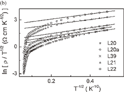
Fig. 10. Plots of ln(ρ/T−1/4) vs T−1/4 (a) and ln(ρ/T−1/2) vs T−1/2 (b) in the p-type β-FeSi2 single crystals doped with Mn.71) The straight lines are linear fits.
Download figure:
Standard image High-resolution imageIn the Cr-doped samples, grown from both the stoichiometric (FeSi2) and non-stoichiometric (FeSi1.5 and FeSi2.5) source compositions, the obtained values of T04 = 310–11600 K and those of T02 = 13–94 K vary within quite broad intervals, indicating a different proximity of samples to the MIT. In particular, the values of T04 = 3460–11600 K and T02 = 66–94 K for stoichiometric compounds exceed considerably those of T04 = 310–610 K and T02 = 13–31 K, obtained in the non-stoichiometric material. In addition, the values of the ratio Rhop/ξ are less than 1 and vary between 1.2–1.7 in the non-stoichiometric and stoichiometric compounds, respectively. These data imply that, generally, the samples grown from the non-stoichiometric source material lie much closer to the MIT than the samples obtained from the stoichiometric source and having the same Cr doping level.70) Eventually, the widths of the impurity (acceptor) band W = 6.0–9.9 meV and of the soft Coulomb gap, Δ = 0.38–1.31 meV, have been determined. It can be seen, that Δ displays large variation in agreement with different proximity of the investigated Cr-doped p-type β-FeSi2 samples to the MIT.70)
In the Co-doped n-type β-FeSi2 samples, the situation with the proximity to the MIT is similar to that discussed above.71) Indeed, the non-stoichiometric (FeSi1.5 and FeSi2.5) compounds yield the values of T04 = 165–1250 K and T02 = 16–40 K, whereas those of the stoichiometric material, T04 = 2400–9700 K and T02 = 40–150 K are substantially higher at a comparable Co doping level. This indicates a shift of the samples, obtained from the stoichiometric source material, apart from the MIT towards the insulating state.71) The values of Δ = 0.5–1.6 meV, comparable with those in the Cr-doped samples,70) reflect a different closeness to the MIT, as well. On the other hand, the variation of W = 3.3–18.2 meV in the Co-doped samples is much higher than in the Cr-doped material,70) indicating a corresponding high variation of the microscopic lattice disorder.65,66)
The Mn-doped p-type β-FeSi2 exhibits a closeness to the MIT for all investigated samples with a minor dependence on the source stoichiometry, yielding T04 = 120–410 K and T02 = 8.2–11.9 K.72) The values of Δ = 0.33–0.40 meV support the inference made above, whereas those of W = 4.9–8.3 meV suggest the different microscopic disorder in the investigated samples, as well.72) For sample #L20, the values of ξ ≈ 74 Å, ξ0 ≈ 7.5 Å (the localization radius far from the MIT, i.e., at NA ≪ Nc), κ ≈ 660, Nc ≈ 3.7 × 1019 cm−3, and g(EF) ≈ 2.4 × 10¹⁸ meV−1·cm−3 have been obtained at NA ≈ 3.3 × 1018 cm−3.72) The values of ξ ≫ ξ0 and κ ≫ κ0 (where κ0 = 29.9 is the value of the dielectric permittivity far from the MIT)73) support the close proximity to the MIT, which is in agreement with the relations NA ∼ Nc, ξ = ξ0 (1 − NA/Nc)−ν and κ = κ0 (1 − NA/Nc)−η,74–76) where ν and η are the critical exponents of the localization radius and the dielectric permittivity, respectively.74–76) However, the ratio of η/ν = 1.35 ± 0.12 obtained in Ref. 75 looks too small, contradicting to the theoretical value, η/ν = 2.77,78) The possible reason of this issue will be discussed further.
An interesting feature of the DOS spectrum of the localized carriers in β-FeSi2 doped with Co, Cr, and Mn follows from a combined analysis of the obtained values of T04, T02, Δ, and W.70–72) Indeed, it can be demonstrated that the parameters T04, T02, and Δ are not independent, but are interrelated with the expression

where C = 135 K2/meV2 is the universal constant.70–72) In particular, it has been shown that Eq. (6) is fulfilled with a reasonable accuracy in amorphous RexSi1−x thin films for Δ ∼ 0.01–1 meV and  K2, supporting Eq. (6) within two decades of Δ and four decades of
  .79) However, in the β-FeSi2 single crystals, doped with Cr, Co, and Mn, Eq. (6) is violated. The examples of such a violation are displayed in Fig. 11.

Download figure:
Standard image High-resolution image
Fig. 11. Plots of  vs Δ2 (×) and (Δ − δ)2 (○) in the Cr-doped (a)70) and Mn-doped (b)72) β-FeSi2 single crystals.
Download figure:
Standard image High-resolution imageNamely, in the Cr-doped material the plot of  vs Δ2 is close to linearity for the majority of samples [Fig. 11(a)], yielding, however, the value of C ≈ 90 K2/meV2 which is a 1.5 times smaller than predicted. In addition, two other samples exhibit a considerable deviation from the linearity. In the Mn-doped samples [Fig. 11(b)] the linearity of the plot of
  vs Δ2 is poor, whereas its linear fit yields C ≈ 110 K2/meV2 and the extrapolation of the straight line to Δ2 = 0 lies far from the origin. At the same time, a strong deviation for one of the samples from the behavior of other samples is observed, as well. Eventually, similar (although less drastic) contradictions with respect to Eq. (6) were observed in the n-type Co-doped β-FeSi2 single crystals.71)
The issue above has been interpreted by existence of the rigid gap δ inside the soft Coulomb gap Δ, in the DOS spectrum of the localized states, i.e., δ < Δ. The Coulomb correlations of charge carriers lead to a parabolic dependence of the DOS g(ε) on the energy ε, g(ε) ∼ (ε − EF)2, so that the "soft" Coulomb gap means that DOS vanishes only at ε = EF.65) On the other hand, the "rigid" (or "hard") gap means that g(ε) = 0 inside a finite energy interval  around EF. The reason to the rigid gap has been attributed to a polaronic nature of charge carriers in β-FeSi2.70–72) Indeed, small polarons were used to interpret the high-temperature transport of the n-type β-FeSi2 doped with Co,32,34) Ni,34) and B,80) as well as the p-type β-FeSi2 doped with Mn,81) and the RT optical properties of undoped β-FeSi2 (Ref. 73). Therefore, to jump from one site to another, a carrier should annihilate polarization of a medium around the initial site and create it around the final site.66) This process is connected with an additional work, yielding a minimum possible energy for hopping, which leads to δ.70–72) An important condition is a requirement of Ed < Ep,70–72) where Ed is width of distribution of the electron potential energy due to the lattice disorder and Ep is depth of the polaron potential well (see the inset to Fig. 12).

Fig. 12. Plots of δ vs W for the β-FeSi2 samples doped with Co (●)71) and Cr (△).70) Inset: Schematic representation of the polaronic potential well.71)
Download figure:
Standard image High-resolution imageExistence of δ modifies Eq. (6) to  ,82) which permits determination of the δ values.70–72) As can be seen in Fig. 12, δ displays a regular dependence on W.71,72) The reason to a maximum of the function δ(W) in Fig. 12 is connected with a competition between the two terms in the expression of δ = Ep/2 − Ed/2 (following from the inset to Fig. 12), both increasing when W is increased due to the lattice disorder, Ed.68) Here, the growth of Ep with Ed is connected to enhanced localization of the charge carriers and, therefore, to a stronger polarization of the medium by them. Eventually, when Ed and Ep become comparable, the rigid gap is washed out,65) as can be seen in Fig. 12 (δ → 0 for highest W).
The assumption, that the charge carriers of β-FeSi2 are small polarons, can clarify the issue of the small value of the ratio η/ν = 1.35 ± 0.12,72) obtained for one of the Mn-doped samples mentioned above. First of all, it can be seen that the value of ξ0 ≈ 7.5 Å for this material satisfy the condition for the small-polaron radius,  , where the maximum radius of the small polaron far from the MIT is given by the relation
 ![$r_{\text{p}}^{\text{max}} = 0.5[\pi /(6N_{\text{A}})]^{1/3} \approx 12.6$](https://content.cld.iop.org/journals/1347-4065/54/7S2/07JA02/revision1/SL14005Rif013.gif) Å.66) Then, taking into account the small-polaron nature of the charge carriers, the analysis in Ref. 75 yields η/ν = 1.66 ± 0.13, which looks more realistic being closer to the theoretical prediction, η/ν = 2.
Å.66) Then, taking into account the small-polaron nature of the charge carriers, the analysis in Ref. 75 yields η/ν = 1.66 ± 0.13, which looks more realistic being closer to the theoretical prediction, η/ν = 2.
Generally, it can be seen a large scattering of ξ, κ, and g(EF), obtained for various materials addressed to the one and the same compound, β-FeSi2 [cf. ξ ≈ 74 Å67,72) and ξ ∼ 1000 Å,69), κ ≈ 27–17069) and κ ≈ 660,72) g(EF) = (280–1.1) × 1019 meV−1·cm−3 in Ref. 68 and g(EF) ∼ 1015 meV−1·cm−3 in Ref. 69]. However, this does not look too surprising (at least for the p-type material), taking into account various types of acceptors with quite different energies and concentrations (Table I), as well as a possible different proximity to the MIT of a system with even a same type of acceptors. Therefore, different acceptor levels (bands) can be involved in the hopping process, depending on the position of EF with respect to these bands and/or to the mobility threshold.66) In turn, position of EF is determined by the impurity concentration and the degree of the compensation, which are sensitive to the state of investigated materials (bulk crystals or thin films), as well as to doping elements and preparation details.
Finally, a scaling behavior of the resistivity according to the law

has been predicted in the domain of the VRH charge transfer, where ρ0 = ApT1/p is the prefactor in Eq. (5), A and Tx are sample-dependent constants, whereas f(x) is a universal function.83) As can be seen in Fig. 13 (where AM ≡ A4), the scaling behavior of Eq. (7) is fulfilled for all the investigated β-FeSi2 samples doped with Co, Cr, and Mn within the whole temperature range of the Mott VRH conduction.70–72) The scaling behavior above confirms the transition to the VRH conductivity in the investigated material and permits determination of the critical temperature, corresponding to the crossover of the Mott and the SE VRH conduction regimes,83) which is in a reasonable agreement with the experimental data.70–72)

Fig. 13. Plots of ln(ρ/AMT−1/4)/A vs ln(T/Tx) for β-FeSi2 doped with Cr (a),70) Co (b),71) and Mn (c).72) The solid line is the function f(x) in Eq. (7).
Download figure:
Standard image High-resolution imageTo summarize, VRH conduction has been observed in the n- and p-type β-FeSi2, including polycrystalline thin films and single crystals doped with Al, Co, Cr, and Mn. Detailed investigations of the VRH conductivity in the Mott and the Shklovskii–Efros regimes has yielded an interesting information both on the macroscopic state (correlation between the insulating properties, or closeness to the MIT, and the stoichiometry of the starting materials) and the microscopic parameters, such as the localization radius and density of the localized states, as well as some fine details of the electron (hole) energy spectrum. However, this inference is referred mainly to the bulk single-crystalline materials, whereas thin films of β-FeSi2 are investigated still insufficiently.
6. Magnetoresistance
The relative magnetoresistance (MR), Δρ/ρ ≡ [ρ(H) − ρ(0)]/ρ(0), is one of the transport effects which can yield a valuable information on the electronic properties of semiconductors. MR can be both positive (pMR),65,84,85) Δρ/ρ > 0, and negative (nMR),85–93) Δρ/ρ < 0, or even oscillating.84) However, the sensitivity of nMR or pMR to the details of the electronic structure usually is not high.65,84–93) This can reduce a potential benefit from investigations of MR, and even interpretation of its origin may require a detailed information on the electronic properties of a compound, obtained preliminary.
Probably, the first observations and detailed investigations of MR in β-FeSi2, addressed to the Mott VRH conduction regime in polycrystalline thin films (see Sect. 5), have been reported in Ref. 67. The nMR has been observed between T ∼ 20–4.5 K exhibiting a quadratic dependence on the magnetic field below H ∼ 8 kOe [inset to the top panel of Fig. 14(a)], a square-root dependence on H in higher fields [Figs. 14(a) and 14(b)] and absence of a saturation with increasing magnetic field up to H = 55 kOe.67) In addition, nMR took place both for H parallel, (Δρ/ρ)∥, and perpendicular, (Δρ/ρ)⊥, to the film plate, yielding the maximum value of 17.1% at T = 4.5 K and H = 55 kOe, as well as the relation (Δρ/ρ)⊥ ≤ (Δρ/ρ)∥.67) To interpret the nMR effect, a model of quantum interference (or QI-1 model) between different direct paths, formed due to scattering of hopping charge carriers by intermediate scattering centers in a VRH conduction regime,88–93) has been applied in Ref. 67. Qualitatively, the results of Ref. 67, including the dependences of Δρ/ρ ∼ H2 in low fields and Δρ/ρ ∼ H1/2 in high fields, as well as absence of the saturation of nMR up to H = 55 kOe (estimated values of the saturation field Hc lie between 87–118 kOe) have been found to be in agreement with the corresponding predictions of the QI-1 model. However, the crossover field of the magnetic field asymptotes of MR has not been compared with that following from the QI-1 model, whereas the low-field quadratic dependence of nMR has been predicted by many other models of nMR, addressed to quite different families of compounds.85–88)

Download figure:
Standard image High-resolution image
Fig. 14. Plots of the magnetoresistance Δρ/ρ vs H1/2 in β-FeSi2 polycrystalline thin films. Inset to (a): Δρ/ρ vs H2 (from Ref. 67).
Download figure:
Standard image High-resolution imageAt this point, it is worth mentioning investigations of nMR in the p-type β-FeSi2 single-crystalline layers [Fig. 15(a)], where neither a low-field quadratic behavior, nor a high-field square-root dependence of nMR, as well as saturation, have been established for H up to 50 kOe.94) On the other hand, observations of the AHE in Ref. 94 permitted to ascribe nMR to the spin-dependent scattering effects.86) At the same time, the low-field quadratic asymptote of nMR, observed in polycrystalline p-type β-FeSi2 epitaxial layers, was transformed into a linear behavior of nMR when H was increased already up to ∼4 kOe (bottom panel of Fig. 16).64)

Download figure:
Standard image High-resolution image
Fig. 15. Plots of MR vs B in p-type β-FeSi2 single-crystalline layer (a)94) and in polycrystalline epitaxial layer (b, the lines are quadratic and linear fits).64)
Download figure:
Standard image High-resolution image
Fig. 16. Plots of ln Xρ vs ln H {where ![$X_{\rho } \equiv \ln [\rho (T,H)/\rho (T,0)]$](https://content.cld.iop.org/journals/1347-4065/54/7S2/07JA02/revision1/SL14005Rif014.gif) } for the Mott (curves 1–3) and the SE (curves 4 and 5) VRH conduction regimes. The straight lines are linear fits.95)
} for the Mott (curves 1–3) and the SE (curves 4 and 5) VRH conduction regimes. The straight lines are linear fits.95)
Download figure:
Standard image High-resolution imageThe nMR basically similar to that in the films above, was observed also in the p-type β-FeSi2 single crystals, however, in an extended temperature interval up to T ∼ 50 K.2) A more detailed investigations of nMR in Al-doped p-type single crystals were performed in Ref. 95. Namely, nMR was observed both in the Mott and the SE VRH conduction regimes.95) As can be seen in Fig. 16 (in Ref. 95, the symbol "log" was confused with the symbol "ln", which is correct here), two linear intervals correspond to the quadratic dependence of nMR in low fields and the linear dependence in higher fields.95) The QI-1 model predicts transformation of the quadratic dependence of nMR into the linear one with increasing field, too.88–93) However, the crossover fields evaluated according to the QI-1 model, were found to be on an order of the magnitude lower than those found experimentally.95) In addition, the QI-1 model predicts the maximum and the saturation of nMR, as well as the change of the MR sign with increasing H.88–93) The corresponding field values have been calculated according to this model to lie below H ∼ 12 kOe, the strongest field of Ref. 95. However, no maxima and saturation of nMR, as well as no change of the sign of MR have been observed in the investigated field interval.95)
Therefore, the nMR in Ref. 95 was attributed to another mechanism, predicted by the QI-2 model.87) According to this model, nMR is connected to the quantum interference of the charge carriers hopping along the loops, similar to that acting in heavily doped semiconductors on the metallic side of the MIT.85) Indeed, the QI-1 model was formulated basically for the regime of a strong localization, taking place on the insulating side but far from the MIT (i.e., at NA ≪ Nc and ξ ∼ ξ0).88–93) On the other hand, as has been mentioned in Sect. 5, in the Al-doped p-type β-FeSi2 samples the very large values of ξ ∼ 1000 Å suggest the Anderson localization regime at a close proximity to the MIT, favoring the conditions of the QI-2 model rather than those of the QI-1 model. However, although the critical exponent, ν ≈ 0.4–0.5, found with the application of the QI-2 model to the nMR, is close to that of ν ≈ 0.5 obtained with investigations of the VRH conduction in the same samples in zero magnetic field,69) the value of ν determined in Refs. 69 and 95 looks too small (a theoretical prediction is ν = 1),74–77) requiring a deeper consideration.
Eventually, both MR effects, the nMR below T ∼ 120 K and H < 2–3 kG, transforming into the pMR in higher fields, as well as the purely pMR effect at T ∼ 130–150 K and absence of the MR at 230 K, have been observed in the n-type unintentionally doped β-FeSi2 epitaxial films (see Fig. 17).63) These films have been obtained using a high-purity 5N Fe source, indicating presence of impurities of As, Al and Mn with concentration of 2 × 1017 cm−3, and exhibiting the high Hall mobility ∼400 cm2·V−1·s−1 at 300 K.63) Therefore, the high-temperature pMR in the intermediate (130–150 K) temperature interval has been attributed to the classical (Lorentzian) effect84) of the itinerant electrons in the defect (impurity) band.63)

Fig. 17. Plots of MR vs magnetic field in the n-type β-FeSi2 epitaxial films.63)
Download figure:
Standard image High-resolution image
Hence, the negative magnetoresistance has been observed below T ∼ 20–50 K in the p- and n-type β-FeSi2 thin films, as well as in the p-type β-FeSi2 single crystals, whereas the positive magnetoresistance has been found only in the intermediate region of T ∼ 110–150 K in the n-type β-FeSi2 thin films with the high Hall mobility of the electrons. The reason to the low-temperature nMR is attributable presumably to the orbital quantum interference effects of the hopping charge carriers in the VRH conduction regime, although observations of the anomalous Hall effect in β-FeSi2 cannot rule out a possible influence of the spin-dependent scattering, as well. The classical MR of the impurity band electrons has been used to interpret pMR in the intermediate temperature range.
7. Conclusions
Transport properties of β-FeSi2, reviewed in this paper, have demonstrated a continuous scientific interest of the silicide society to the iron disilicide semiconducting compound. This is connected with a substantial progress achieved in recent time in preparation of the high-quality epitaxial layers and single crystals, including those with the reported high values of the mobility of charge carriers. In turn, this leads to a better understanding of the physical properties of β-FeSi2, including both the macroscopic behavior and the microscopic parameters of the charge carriers, as well as details of the electronic structure. On the other hand, the n-type β-FeSi2 single crystals and films are studied still insufficiently, requiring further investigations to clarify the anomalies of their transport behavior. Nevertheless, the already obtained results confirm the promising prospects for wide applications of β-FeSi2.
Acknowledgments
The authors would like to express sincere gratitude to the organizers of the International conference and summer school on advanced silicide technology (ICSS-Silicide 2014) for their kind invitation to participate the Conference, for the proposal to prepare this review and for the support. We are particularly grateful to Professor T. Suemasu for useful discussions. It is our pleasure to thank Professor Ch. Kloc and Dr. J. Schumann for the fruitful collaboration.